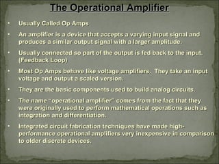
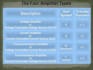
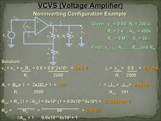
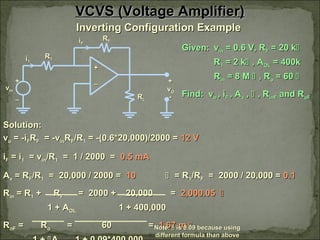
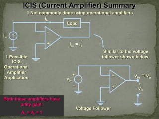
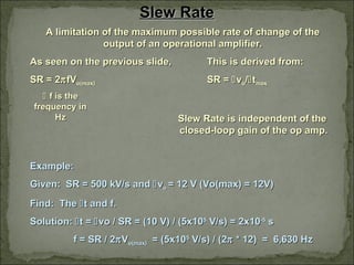
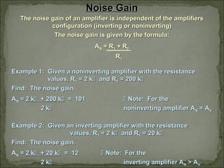
Operational AmplifiersOperational Amplifiers
Submitted by: Preeti choudharySubmitted by: Preeti choudhary
M.Sc.(Applied Physics)M.Sc.(Applied Physics)
ContentsContents
The Operational AmplifierThe Operational Amplifier
The Four Amplifier TypesThe Four Amplifier Types
VCVS(Voltage Amplifier) Summary:VCVS(Voltage Amplifier) Summary:
Noninverting ConfigurationNoninverting Configuration
Inverting ConfigurationInverting Configuration
ICIC(Current Amplifier) SummaryICIC(Current Amplifier) Summary
VCIS (Transconductance Amplifier) SummaryVCIS (Transconductance Amplifier) Summary
ICVS (Transresistance Amplifier) SummaryICVS (Transresistance Amplifier) Summary
Power BandwidthPower Bandwidth
Slew RateSlew Rate
Slew Rate Output DistortionSlew Rate Output Distortion
Noise GainNoise Gain
Gain-Bandwidth ProductGain-Bandwidth Product
Cascaded Amplifiers - BandwidthCascaded Amplifiers - Bandwidth
Common Mode Rejection RatioCommon Mode Rejection Ratio
Power Supply Rejection RatioPower Supply Rejection Ratio
SourcesSources
The Operational AmplifierThe Operational Amplifier
• Usually Called Op AmpsUsually Called Op Amps
• An amplifier is a device that accepts a varying input signal andAn amplifier is a device that accepts a varying input signal and
produces a similar output signal with a larger amplitude.produces a similar output signal with a larger amplitude.
• Usually connected so part of the output is fed back to the input.Usually connected so part of the output is fed back to the input.
(Feedback Loop)(Feedback Loop)
• Most Op Amps behave like voltage amplifiers. They take an inputMost Op Amps behave like voltage amplifiers. They take an input
voltage and output a scaled version.voltage and output a scaled version.
• They are the basic components used to build analog circuits.They are the basic components used to build analog circuits.
• The name “operational amplifier” comes from the fact that theyThe name “operational amplifier” comes from the fact that they
were originally used to perform mathematical operations such aswere originally used to perform mathematical operations such as
integration and differentiation.integration and differentiation.
• Integrated circuit fabrication techniques have made high-Integrated circuit fabrication techniques have made high-
performance operational amplifiers very inexpensive in comparisonperformance operational amplifiers very inexpensive in comparison
to older discrete devices.to older discrete devices.
• ii(+)(+), i, i(-)(-) : Currents into the amplifier on the inverting and noninverting lines: Currents into the amplifier on the inverting and noninverting lines
respectivelyrespectively
• vvidid : The input voltage from inverting to non-inverting inputs: The input voltage from inverting to non-inverting inputs
• +V+VSS , -V, -VSS : DC source voltages, usually +15V and –15V: DC source voltages, usually +15V and –15V
• RRii : The input resistance, ideally infinity: The input resistance, ideally infinity
• A : The gain of the amplifier. Ideally very high, in the 1x10A : The gain of the amplifier. Ideally very high, in the 1x101010
range.range.
• RROO: The output resistance, ideally zero: The output resistance, ideally zero
• vvOO: The output voltage; v: The output voltage; vOO = A= AOLOLvvidid where Awhere AOLOL is the open-loop voltage gainis the open-loop voltage gain
The Operational AmplifierThe Operational Amplifier
+V+VSS
-V-VSS
vvidid
InvertingInverting
NoninvertingNoninverting
OutputOutput
++
__ii(-)(-)
ii(+)(+)
vvOO = A= Addvvidid
RROO
AA
RRii
The Four Amplifier TypesThe Four Amplifier Types
Description
Gain
Symbol
Transfer
Function
Voltage Amplifier
or
Voltage Controlled Voltage Source (VCVS)
Av vo/vin
Current Amplifier
or
Current Controlled Current Source (ICIS)
Ai io/iin
Transconductance Amplifier
or
Voltage Controlled Current Source (VCIS)
gm
(siemens)
io/vin
Transresistance Amplifier
or
Current Controlled Voltage Source (ICVS)
rm
(ohms)
vo/iin
VCVS (Voltage Amplifier) SummaryVCVS (Voltage Amplifier) Summary
Noninverting ConfigurationNoninverting Configuration
++
__
vvinin
++
++
--
vvOO
vvidid
ii(+)(+)
ii(-)(-)
iiOO
iiFF
RRFF RRLL
RR11
ii11
vvidid = v= voo/A/AOLOL
Assuming AAssuming AOLOL  
vvidid =0=0
Also, with theAlso, with the
assumption that Rassumption that Rinin == 
ii(+)(+) = i= i(-)(-) = 0= 0
__
vvFF
++
__
vv11
++
__
vvLL
++
__
iiLL
Applying KVL theApplying KVL the
following equationsfollowing equations
can be found:can be found:
vv11 = v= vinin
vvOO = v= v11 + v+ vFF = v= vinin+ i+ iFFRRFF
This means that,This means that,
iiFF = i= i11
Therefore: iTherefore: iFF = v= vinin/R/R11
Using the equation to the left the outputUsing the equation to the left the output
voltage becomes:voltage becomes:
vvoo = v= vinin + v+ vininRRFF = v= vinin RRFF + 1+ 1
RR11 RR11
VCVS (Voltage Amplifier) SummaryVCVS (Voltage Amplifier) Summary
Noninverting Configuration ContinuedNoninverting Configuration Continued
The closed-loop voltage gain is symbolized by AThe closed-loop voltage gain is symbolized by Avv and is found to be:and is found to be:
AAvv = v= voo = R= RFF + 1+ 1
vvinin RR11
The original closed loop gain equation is:The original closed loop gain equation is:
AAvv = A= AFF = A= AOLOL
1 + A1 + AOLOL
Ideally AIdeally AOLOL   , Therefore A, Therefore Avv = 1= 1

Note: The actual value of ANote: The actual value of AOLOL is given for the specific device andis given for the specific device and
usually ranges from 50kusually ranges from 50k  500k.500k.
 is the feedback factor and by assuming open-loop gain is infinite:is the feedback factor and by assuming open-loop gain is infinite:
 = R= R11
RR11 + R+ RFF
AAFF is the amplifieris the amplifier
gain withgain with
feedbackfeedback
VCVS (Voltage Amplifier) SummaryVCVS (Voltage Amplifier) Summary
Noninverting Configuration ContinuedNoninverting Configuration Continued
Input and Output ResistanceInput and Output Resistance
Ideally, the input resistance for this configuration is infinity, but the aIdeally, the input resistance for this configuration is infinity, but the a
closer prediction of the actual input resistance can be found with thecloser prediction of the actual input resistance can be found with the
following formula:following formula:
RRinFinF = R= Rinin (1 +(1 + AAOLOL)) Where RWhere Rinin is given for theis given for the
specified device. Usually Rspecified device. Usually Rinin isis
in the Min the M range.range.
Ideally, the output resistance is zero, but the formula below gives aIdeally, the output resistance is zero, but the formula below gives a
more accurate value:more accurate value:
RRoFoF = R= Roo Where RWhere Roo is given for theis given for the
AAOLOL + 1+ 1 specified device. Usually Rspecified device. Usually Roo is inis in
the 10the 10ss
ofof ss
range.range.
VCVS (Voltage Amplifier)VCVS (Voltage Amplifier)
Noninverting Configuration ExampleNoninverting Configuration Example
++
__
vvinin
++
++
--
vvOO
vvidid
ii(+)(+)
ii(-)(-)
iiOO
iiFF
RRFF RRLL
RR11
ii11
__
vvFF
++
__
vv11
++
__
vvLL
++
__
iiLL
Given:Given: vvinin = 0.6V, R= 0.6V, RFF = 200 k= 200 k
RR11 = 2 k= 2 k , A, AOLOL = 400k= 400k
RRinin = 8 M= 8 M  , R, Roo = 60= 60 
Find: vFind: voo , i, iFF , A, Avv ,,  , R, RinFinF and Rand RoFoF
Solution:Solution:
vvoo = v= vinin + v+ vininRRFF = 0.6 + 0.6*2x10= 0.6 + 0.6*2x1055
== 60.6 V60.6 V iiFF = v= vinin = 0.6 == 0.6 = 0.3 mA0.3 mA
RR11 20002000 RR11 20002000
AAvv = R= RFF + 1 = 2x10+ 1 = 2x1055
+ 1 =+ 1 = 101101  = 1 = 1 == 1 = 1 = 9.9x109.9x10-3-3
RR11 20002000 AAOLOL 101101
RRinFinF = R= Rinin (1 +(1 + AAOLOL) = 8x10) = 8x1066
(1 + 9.9x10(1 + 9.9x10⁻³-3
*4x10*4x1055
) =) = 3.1688x103.1688x101010

RRoFoF = R= Roo = 60= 60 == 0.0150.015 
AAOLOL + 1 9.9x10+ 1 9.9x10⁻³-3
*4x10*4x1055
+ 1+ 1
VCVS (Voltage Amplifier) SummaryVCVS (Voltage Amplifier) Summary
Inverting ConfigurationInverting Configuration
++
__
RRLL
vvOO
++
--
vvinin
++
__
RR11ii11
RRFFiiFF
The sameThe same
assumptions used toassumptions used to
find the equations forfind the equations for
the noninvertingthe noninverting
configuration areconfiguration are
also used for thealso used for the
invertinginverting
configuration.configuration.
General Equations:General Equations:
ii11 = v= vinin/R/R11
iiFF = i= i11
vvoo = -i= -iFFRRFF = -v= -vininRRFF/R/R11
AAvv = R= RFF/R/R11  = R= R11/R/RFF
Input and Output ResistanceInput and Output Resistance
Ideally, the input resistance for this configuration is equivalent to RIdeally, the input resistance for this configuration is equivalent to R11..
However, the actual value of the input resistance is given by theHowever, the actual value of the input resistance is given by the
following formula:following formula:
RRinin = R= R11 + R+ RFF
1 + A1 + AOLOL
Ideally, the output resistance is zero, but the formula below gives aIdeally, the output resistance is zero, but the formula below gives a
more accurate value:more accurate value:
RRoFoF = R= Roo
1 +1 + AAOLOL
Note:Note:  = R= R11 This is different from the equation usedThis is different from the equation used
RR11 + R+ RFF on the previous slide, which can be confusing.on the previous slide, which can be confusing.
VCVS (Voltage Amplifier) SummaryVCVS (Voltage Amplifier) Summary
Inverting Configuration ContinuedInverting Configuration Continued
VCVS (Voltage Amplifier)VCVS (Voltage Amplifier)
Inverting Configuration ExampleInverting Configuration Example
++
__
RRLL
++
--
vvinin
++
__
RR11ii11
RRFFiiFF
Given:Given: vvinin = 0.6 V, R= 0.6 V, RFF = 20 k= 20 k
RR11 = 2 k= 2 k , A, AOLOL = 400k= 400k
RRinin = 8 M= 8 M  , R, Roo = 60= 60 
Find: vFind: voo , i, iFF , A, Avv ,,  , R, RinFinF and Rand RoFoF
vvOO
Solution:Solution:
vvoo = -i= -iFFRRFF = -v= -vininRRFF/R/R11 = -(0.6*20,000)/2000 == -(0.6*20,000)/2000 = 12 V12 V
iiFF = i= i11 = v= vinin/R/R11 = 1 / 2000 == 1 / 2000 = 0.5 mA0.5 mA
AAvv = R= RFF/R/R11 = 20,000 / 2000 == 20,000 / 2000 = 1010  = R= R11/R/RFF = 2000 / 20,000 == 2000 / 20,000 = 0.10.1
RRinin = R= R11 + R+ RFF = 2000 + 20,000= 2000 + 20,000 == 2,000.052,000.05 
1 + A1 + AOLOL 1 + 400,0001 + 400,000
RRoFoF = R= Roo = 60= 60 == 1.67 m1.67 m Note:Note:  is 0.09 because usingis 0.09 because using
different formula than abovedifferent formula than above
ICIS (Current Amplifier) SummaryICIS (Current Amplifier) Summary
 Not commonly done using operational amplifiersNot commonly done using operational amplifiers
++
__
LoadLoad
iiinin
iiLL
Similar to the voltageSimilar to the voltage
follower shown below:follower shown below:
Both these amplifiers haveBoth these amplifiers have
unity gain:unity gain:
AAvv = A= Aii = 1= 1
++
__
iiinin = i= iLL
vvinin = v= voo
vvinin
++
__ ++
--
vvOO
Voltage FollowerVoltage Follower
1 Possible1 Possible
ICISICIS
OperationalOperational
AmplifierAmplifier
ApplicationApplication
VCIS (Transconductance Amplifier) SummaryVCIS (Transconductance Amplifier) Summary
Voltage to Current ConverterVoltage to Current Converter
++
__
LoadLoad
iiLL
RR11ii11
vvinin
++
__
OROR
++
__
LoadLoad
iiLL
RR11ii11
vvinin
++
__
vvinin
++
__
General Equations:General Equations:
iiLL = i= i11 = v= v11/R/R11
vv11 = v= vinin
The transconductance, gThe transconductance, gmm = i= ioo/v/vinin = 1/R= 1/R11
Therefore, iTherefore, iLL = i= i11 = v= vinin/R/R11 = g= gmmvvinin
The maximum load resistance is determined by:The maximum load resistance is determined by:
RRL(max)L(max) = v= vo(max)o(max)/i/iLL
VCIS (Transconductance Amplifier)VCIS (Transconductance Amplifier)
Voltage to Current Converter ExampleVoltage to Current Converter Example
++
__
LoadLoad
iiLL
RR11ii11
vvinin
++
__
Given: vGiven: vinin = 2 V, R= 2 V, R11 = 2 k= 2 k
vvo(max)o(max) ==  10 V10 V
Find: iFind: iLL , g, gmm and Rand RL(max)L(max)
Solution:Solution:
iiLL = i= i11 = v= vinin/R/R11 = 2 / 2000 == 2 / 2000 = 1 mA1 mA
ggmm = i= ioo/v/vinin = 1/R= 1/R11 = 1 / 2000 == 1 / 2000 = 0.5 mS0.5 mS
RRL(max)L(max) = v= vo(max)o(max)/i/iLL = 10 V / 1 mA= 10 V / 1 mA
== 10 k10 k 
Note:Note:
• If RIf RLL > R> RL(max)L(max) the op ampthe op amp
will saturatewill saturate
• The output current, iThe output current, iLL isis
independent of the loadindependent of the load
resistance.resistance.
VCIS (Transresistance Amplifier) SummaryVCIS (Transresistance Amplifier) Summary
Current to Voltage ConverterCurrent to Voltage Converter
General Equations:General Equations:
iiFF = i= iinin
vvoo = -i= -iFFRRFF
rrmm = v= voo/i/iinin = R= RFF
++
__
iiFF
iiinin
RRFF
vvOO
++
--
VCIS (Transresistance Amplifier) SummaryVCIS (Transresistance Amplifier) Summary
Current to Voltage ConverterCurrent to Voltage Converter
• Transresistance Amplifiers are used for low-powerTransresistance Amplifiers are used for low-power
applications to produce an output voltage proportional toapplications to produce an output voltage proportional to
the input current.the input current.
• Photodiodes and Phototransistors, which are used in thePhotodiodes and Phototransistors, which are used in the
production of solar power are commonly modeled asproduction of solar power are commonly modeled as
current sources.current sources.
• Current to Voltage Converters can be used to convert theseCurrent to Voltage Converters can be used to convert these
current sources to more commonly used voltage sources.current sources to more commonly used voltage sources.
VCIS (Transresistance Amplifier)VCIS (Transresistance Amplifier)
Current to Voltage Converter ExampleCurrent to Voltage Converter Example
++
__
iiFF
iiinin
RRFF
vvOO
++
--
Given: iGiven: iinin = 10 mA= 10 mA
RRFF = 200= 200 
Find: iFind: iFF , v, voo and rand rmm
Solution:Solution:
iiFF = i= iinin == 10 mA10 mA
vvoo = -i= -iFFRRFF = 10 mA * 200= 10 mA * 200  == 2 V2 V
rrmm = v= voo/i/iinin = R= RFF == 200200
Power BandwidthPower Bandwidth
The maximum frequency at which a sinusoidal output signal can beThe maximum frequency at which a sinusoidal output signal can be
produced without causing distortion in the signal.produced without causing distortion in the signal.
The power bandwidth, BWThe power bandwidth, BWpp is determined using the desiredis determined using the desired
output signal amplitude and the the slew rate (output signal amplitude and the the slew rate (see next slidesee next slide))
specifications of the op amp.specifications of the op amp.
BWBWpp = SR= SR
22ππVVo(max)o(max)
SR = 2SR = 2ππfVfVo(max)o(max) where SR is the slew ratewhere SR is the slew rate
Example:Example:
Given: VGiven: Vo(max)o(max) = 12 V and SR = 500 kV/s= 12 V and SR = 500 kV/s
Find: BWFind: BWpp
Solution:Solution: BWBWpp == 500 kV/s500 kV/s = 6.63 kHz= 6.63 kHz
22ππ * 12 V* 12 V
Slew RateSlew Rate
A limitation of the maximum possible rate of change of theA limitation of the maximum possible rate of change of the
output of an operational amplifier.output of an operational amplifier.
As seen on the previous slide,As seen on the previous slide, This is derived from:This is derived from:
SR = 2SR = 2ππfVfVo(max)o(max) SR =SR = vvoo//ttmaxmax
Slew Rate is independent of theSlew Rate is independent of the
closed-loop gain of the op amp.closed-loop gain of the op amp.
Example:Example:
Given: SR = 500 kV/s andGiven: SR = 500 kV/s and vvoo = 12 V (Vo(max) = 12V)= 12 V (Vo(max) = 12V)
Find: TheFind: The t and f.t and f.
Solution:Solution: t =t = vo / SR = (10 V) / (5x10vo / SR = (10 V) / (5x1055
V/s) = 2x10V/s) = 2x10⁻⁵-5
ss
f = SR / 2f = SR / 2ππVVo(max)o(max) = (5x10= (5x1055
V/s) / (2V/s) / (2ππ * 12) = 6,630 Hz* 12) = 6,630 Hz
 f is thef is the
frequency infrequency in
HzHz
Slew Rate DistortionSlew Rate Distortion
vv
tt
desired outputdesired output
waveformwaveform
actual outputactual output
because ofbecause of
slew rateslew rate
limitationlimitation
 tt
vv
The picture above shows exactly what happens when theThe picture above shows exactly what happens when the
slew rate limitations are not met and the output of theslew rate limitations are not met and the output of the
operational amplifier is distorted.operational amplifier is distorted.
SR =SR = v/v/t = m (slope)t = m (slope)
Noise GainNoise Gain
The noise gain of an amplifier is independent of the amplifiersThe noise gain of an amplifier is independent of the amplifiers
configuration (inverting or noninverting)configuration (inverting or noninverting)
The noise gain is given by the formula:The noise gain is given by the formula:
AANN = R= R11 + R+ RFF
RR11
Example 1: Given a noninverting amplifier with the resistanceExample 1: Given a noninverting amplifier with the resistance
values, Rvalues, R11 = 2 k= 2 k and Rand RFF = 200 k= 200 k
Find: The noise gain.Find: The noise gain.
AANN == 2 k2 k + 200 k+ 200 k = 101= 101  Note: For theNote: For the
2 k2 k noninverting amplifier Anoninverting amplifier ANN = A= AVV
Example 2: Given an inverting amplifier with the resistanceExample 2: Given an inverting amplifier with the resistance
values, Rvalues, R11 = 2 k= 2 k and Rand RFF = 20 k= 20 k
Find: The noise gain.Find: The noise gain.
AANN == 2 k2 k + 20 k+ 20 k = 12= 12  Note: For theNote: For the
2 k2 k inverting amplifier Ainverting amplifier ANN > A> AVV
Gain-Bandwidth ProductGain-Bandwidth Product
In most operational amplifiers, the open-loop gain beginsIn most operational amplifiers, the open-loop gain begins
dropping off at very low frequencies. Therefore, to make thedropping off at very low frequencies. Therefore, to make the
op amp useful at higher frequencies, gain is traded forop amp useful at higher frequencies, gain is traded for
bandwidth.bandwidth.
The Gain-Bandwidth Product (GBW) is given by:The Gain-Bandwidth Product (GBW) is given by:
GBW = AGBW = ANNBWBW
Example: For a 741 op amp, a noise gain of 10 k correspondsExample: For a 741 op amp, a noise gain of 10 k corresponds
to a bandwidth of ~200 Hzto a bandwidth of ~200 Hz
Find: The GBWFind: The GBW
GBW = 10 k * 200 Hz = 2 MHzGBW = 10 k * 200 Hz = 2 MHz
Cascaded Amplifiers - BandwidthCascaded Amplifiers - Bandwidth
Quite often, one amplifier does not increase the signal enoughQuite often, one amplifier does not increase the signal enough
and amplifiers are cascaded so the output of one amplifier is theand amplifiers are cascaded so the output of one amplifier is the
input to the next.input to the next.
The amplifiers are matched so:The amplifiers are matched so:
BWBWSS = BW= BW11 = BW= BW22 == GBWGBW where, BWwhere, BWSS is the bandwidth of allis the bandwidth of all
AANN the cascaded amplifiers and Athe cascaded amplifiers and ANN isis
the noise gainthe noise gain
The Total Bandwidth of the Cascaded Amplifiers is:The Total Bandwidth of the Cascaded Amplifiers is:
BWBWTT = BW= BWss(2(21/n1/n
– 1)– 1)1/21/2
where n is the number of amplifierswhere n is the number of amplifiers
that are being cascadedthat are being cascaded
Example: Cascading 3 Amplifiers with GBW = 1 MHz and AExample: Cascading 3 Amplifiers with GBW = 1 MHz and ANN = 15,= 15,
Find: The Total Bandwidth, BWFind: The Total Bandwidth, BWTT
BWBWSS = 1 MHz / 15 = 66.7 kHz= 1 MHz / 15 = 66.7 kHz
BWBWTT = 66.7 kHz (2= 66.7 kHz (21/31/3
– 1)– 1)1/21/2
= 34 kHz= 34 kHz
Common-Mode Rejection RatioCommon-Mode Rejection Ratio
The common-mode rejection ratio (CMRR) relates to the ability ofThe common-mode rejection ratio (CMRR) relates to the ability of
the op amp to reject common-mode input voltage. This is verythe op amp to reject common-mode input voltage. This is very
important because common-mode signals are frequentlyimportant because common-mode signals are frequently
encountered in op amp applications.encountered in op amp applications.
CMRR = 20 log|ACMRR = 20 log|ANN / A/ Acmcm||
AAcmcm == AANN
loglog-1-1
(CMRR / 20)(CMRR / 20)
We solve for AWe solve for Acmcm because Op Amp data sheets list the CMRR value.because Op Amp data sheets list the CMRR value.
The common-mode input voltage is an average of the voltages thatThe common-mode input voltage is an average of the voltages that
are present at the non-inverting and inverting terminals of theare present at the non-inverting and inverting terminals of the
amplifier.amplifier.
vvicmicm = v= v(+)(+) + v+ v(-)(-)
22
Common-Mode Rejection RatioCommon-Mode Rejection Ratio
ExampleExample
Given: A 741 op amp with CMRR = 90 dB and a noise gain,Given: A 741 op amp with CMRR = 90 dB and a noise gain,
AANN = 1 k= 1 k
Find: The common mode gain, AFind: The common mode gain, Acmcm
AAcmcm == AANN = 1000= 1000
loglog-1-1
(CMRR / 20)(CMRR / 20) loglog-1-1
(90 / 20)(90 / 20)
= 0.0316= 0.0316
It is very desirable for the common-mode gain to be small.It is very desirable for the common-mode gain to be small.
Power Supply Rejection RatioPower Supply Rejection Ratio
One of the reasons op amps are so useful, is that they canOne of the reasons op amps are so useful, is that they can
be operated from a wide variety of power supply voltages.be operated from a wide variety of power supply voltages.
The 741 op amp can be operated from bipolar suppliesThe 741 op amp can be operated from bipolar supplies
ranging from 5V to 18V with out too many changes to theranging from 5V to 18V with out too many changes to the
parameters of the op amp.parameters of the op amp.
The power supply rejection ratio (SVRR) refers to the slightThe power supply rejection ratio (SVRR) refers to the slight
change in output voltage that occurs when the powerchange in output voltage that occurs when the power
supply of the op amp changes during operation.supply of the op amp changes during operation.
SVRR = 20 log (VSVRR = 20 log (Vss / V/ Voo))
The SVRR value is given for a specified op amp. For theThe SVRR value is given for a specified op amp. For the
741 op amp, SVRR = 96 dB over the range 5V to 18V.741 op amp, SVRR = 96 dB over the range 5V to 18V.
Open-Loop Op Amp CharacteristicsOpen-Loop Op Amp Characteristics
Device LM741C LF351 OP-07 LH0003 AD549K
Technology BJT BiFET BJT
Hybrid
BJT
BiFET
AOL(typ) 200 k 100 k 400 k 40 k 100 k
Rin 2 M 1012
 8 M 100 k 1013
 || 1 pF
Ro 50  30  60  50  ~100 
SR 0.5 V/µs 13 V/µs 0.3 V/µs 70 V/µs 3 V/µs
CMRR 90 dB 100 dB 110 dB 90 dB 90 dB
Thank youThank you

Operational amplifiers

  • 1.
    Operational AmplifiersOperational Amplifiers Submittedby: Preeti choudharySubmitted by: Preeti choudhary M.Sc.(Applied Physics)M.Sc.(Applied Physics)
  • 2.
    ContentsContents The Operational AmplifierTheOperational Amplifier The Four Amplifier TypesThe Four Amplifier Types VCVS(Voltage Amplifier) Summary:VCVS(Voltage Amplifier) Summary: Noninverting ConfigurationNoninverting Configuration Inverting ConfigurationInverting Configuration ICIC(Current Amplifier) SummaryICIC(Current Amplifier) Summary VCIS (Transconductance Amplifier) SummaryVCIS (Transconductance Amplifier) Summary ICVS (Transresistance Amplifier) SummaryICVS (Transresistance Amplifier) Summary Power BandwidthPower Bandwidth Slew RateSlew Rate Slew Rate Output DistortionSlew Rate Output Distortion Noise GainNoise Gain Gain-Bandwidth ProductGain-Bandwidth Product Cascaded Amplifiers - BandwidthCascaded Amplifiers - Bandwidth Common Mode Rejection RatioCommon Mode Rejection Ratio Power Supply Rejection RatioPower Supply Rejection Ratio SourcesSources
  • 3.
    The Operational AmplifierTheOperational Amplifier • Usually Called Op AmpsUsually Called Op Amps • An amplifier is a device that accepts a varying input signal andAn amplifier is a device that accepts a varying input signal and produces a similar output signal with a larger amplitude.produces a similar output signal with a larger amplitude. • Usually connected so part of the output is fed back to the input.Usually connected so part of the output is fed back to the input. (Feedback Loop)(Feedback Loop) • Most Op Amps behave like voltage amplifiers. They take an inputMost Op Amps behave like voltage amplifiers. They take an input voltage and output a scaled version.voltage and output a scaled version. • They are the basic components used to build analog circuits.They are the basic components used to build analog circuits. • The name “operational amplifier” comes from the fact that theyThe name “operational amplifier” comes from the fact that they were originally used to perform mathematical operations such aswere originally used to perform mathematical operations such as integration and differentiation.integration and differentiation. • Integrated circuit fabrication techniques have made high-Integrated circuit fabrication techniques have made high- performance operational amplifiers very inexpensive in comparisonperformance operational amplifiers very inexpensive in comparison to older discrete devices.to older discrete devices.
  • 4.
    • ii(+)(+), i,i(-)(-) : Currents into the amplifier on the inverting and noninverting lines: Currents into the amplifier on the inverting and noninverting lines respectivelyrespectively • vvidid : The input voltage from inverting to non-inverting inputs: The input voltage from inverting to non-inverting inputs • +V+VSS , -V, -VSS : DC source voltages, usually +15V and –15V: DC source voltages, usually +15V and –15V • RRii : The input resistance, ideally infinity: The input resistance, ideally infinity • A : The gain of the amplifier. Ideally very high, in the 1x10A : The gain of the amplifier. Ideally very high, in the 1x101010 range.range. • RROO: The output resistance, ideally zero: The output resistance, ideally zero • vvOO: The output voltage; v: The output voltage; vOO = A= AOLOLvvidid where Awhere AOLOL is the open-loop voltage gainis the open-loop voltage gain The Operational AmplifierThe Operational Amplifier +V+VSS -V-VSS vvidid InvertingInverting NoninvertingNoninverting OutputOutput ++ __ii(-)(-) ii(+)(+) vvOO = A= Addvvidid RROO AA RRii
  • 5.
    The Four AmplifierTypesThe Four Amplifier Types Description Gain Symbol Transfer Function Voltage Amplifier or Voltage Controlled Voltage Source (VCVS) Av vo/vin Current Amplifier or Current Controlled Current Source (ICIS) Ai io/iin Transconductance Amplifier or Voltage Controlled Current Source (VCIS) gm (siemens) io/vin Transresistance Amplifier or Current Controlled Voltage Source (ICVS) rm (ohms) vo/iin
  • 6.
    VCVS (Voltage Amplifier)SummaryVCVS (Voltage Amplifier) Summary Noninverting ConfigurationNoninverting Configuration ++ __ vvinin ++ ++ -- vvOO vvidid ii(+)(+) ii(-)(-) iiOO iiFF RRFF RRLL RR11 ii11 vvidid = v= voo/A/AOLOL Assuming AAssuming AOLOL   vvidid =0=0 Also, with theAlso, with the assumption that Rassumption that Rinin ==  ii(+)(+) = i= i(-)(-) = 0= 0 __ vvFF ++ __ vv11 ++ __ vvLL ++ __ iiLL Applying KVL theApplying KVL the following equationsfollowing equations can be found:can be found: vv11 = v= vinin vvOO = v= v11 + v+ vFF = v= vinin+ i+ iFFRRFF This means that,This means that, iiFF = i= i11 Therefore: iTherefore: iFF = v= vinin/R/R11 Using the equation to the left the outputUsing the equation to the left the output voltage becomes:voltage becomes: vvoo = v= vinin + v+ vininRRFF = v= vinin RRFF + 1+ 1 RR11 RR11
  • 7.
    VCVS (Voltage Amplifier)SummaryVCVS (Voltage Amplifier) Summary Noninverting Configuration ContinuedNoninverting Configuration Continued The closed-loop voltage gain is symbolized by AThe closed-loop voltage gain is symbolized by Avv and is found to be:and is found to be: AAvv = v= voo = R= RFF + 1+ 1 vvinin RR11 The original closed loop gain equation is:The original closed loop gain equation is: AAvv = A= AFF = A= AOLOL 1 + A1 + AOLOL Ideally AIdeally AOLOL   , Therefore A, Therefore Avv = 1= 1  Note: The actual value of ANote: The actual value of AOLOL is given for the specific device andis given for the specific device and usually ranges from 50kusually ranges from 50k  500k.500k.  is the feedback factor and by assuming open-loop gain is infinite:is the feedback factor and by assuming open-loop gain is infinite:  = R= R11 RR11 + R+ RFF AAFF is the amplifieris the amplifier gain withgain with feedbackfeedback
  • 8.
    VCVS (Voltage Amplifier)SummaryVCVS (Voltage Amplifier) Summary Noninverting Configuration ContinuedNoninverting Configuration Continued Input and Output ResistanceInput and Output Resistance Ideally, the input resistance for this configuration is infinity, but the aIdeally, the input resistance for this configuration is infinity, but the a closer prediction of the actual input resistance can be found with thecloser prediction of the actual input resistance can be found with the following formula:following formula: RRinFinF = R= Rinin (1 +(1 + AAOLOL)) Where RWhere Rinin is given for theis given for the specified device. Usually Rspecified device. Usually Rinin isis in the Min the M range.range. Ideally, the output resistance is zero, but the formula below gives aIdeally, the output resistance is zero, but the formula below gives a more accurate value:more accurate value: RRoFoF = R= Roo Where RWhere Roo is given for theis given for the AAOLOL + 1+ 1 specified device. Usually Rspecified device. Usually Roo is inis in the 10the 10ss ofof ss range.range.
  • 9.
    VCVS (Voltage Amplifier)VCVS(Voltage Amplifier) Noninverting Configuration ExampleNoninverting Configuration Example ++ __ vvinin ++ ++ -- vvOO vvidid ii(+)(+) ii(-)(-) iiOO iiFF RRFF RRLL RR11 ii11 __ vvFF ++ __ vv11 ++ __ vvLL ++ __ iiLL Given:Given: vvinin = 0.6V, R= 0.6V, RFF = 200 k= 200 k RR11 = 2 k= 2 k , A, AOLOL = 400k= 400k RRinin = 8 M= 8 M  , R, Roo = 60= 60  Find: vFind: voo , i, iFF , A, Avv ,,  , R, RinFinF and Rand RoFoF Solution:Solution: vvoo = v= vinin + v+ vininRRFF = 0.6 + 0.6*2x10= 0.6 + 0.6*2x1055 == 60.6 V60.6 V iiFF = v= vinin = 0.6 == 0.6 = 0.3 mA0.3 mA RR11 20002000 RR11 20002000 AAvv = R= RFF + 1 = 2x10+ 1 = 2x1055 + 1 =+ 1 = 101101  = 1 = 1 == 1 = 1 = 9.9x109.9x10-3-3 RR11 20002000 AAOLOL 101101 RRinFinF = R= Rinin (1 +(1 + AAOLOL) = 8x10) = 8x1066 (1 + 9.9x10(1 + 9.9x10⁻³-3 *4x10*4x1055 ) =) = 3.1688x103.1688x101010  RRoFoF = R= Roo = 60= 60 == 0.0150.015  AAOLOL + 1 9.9x10+ 1 9.9x10⁻³-3 *4x10*4x1055 + 1+ 1
  • 10.
    VCVS (Voltage Amplifier)SummaryVCVS (Voltage Amplifier) Summary Inverting ConfigurationInverting Configuration ++ __ RRLL vvOO ++ -- vvinin ++ __ RR11ii11 RRFFiiFF The sameThe same assumptions used toassumptions used to find the equations forfind the equations for the noninvertingthe noninverting configuration areconfiguration are also used for thealso used for the invertinginverting configuration.configuration. General Equations:General Equations: ii11 = v= vinin/R/R11 iiFF = i= i11 vvoo = -i= -iFFRRFF = -v= -vininRRFF/R/R11 AAvv = R= RFF/R/R11  = R= R11/R/RFF
  • 11.
    Input and OutputResistanceInput and Output Resistance Ideally, the input resistance for this configuration is equivalent to RIdeally, the input resistance for this configuration is equivalent to R11.. However, the actual value of the input resistance is given by theHowever, the actual value of the input resistance is given by the following formula:following formula: RRinin = R= R11 + R+ RFF 1 + A1 + AOLOL Ideally, the output resistance is zero, but the formula below gives aIdeally, the output resistance is zero, but the formula below gives a more accurate value:more accurate value: RRoFoF = R= Roo 1 +1 + AAOLOL Note:Note:  = R= R11 This is different from the equation usedThis is different from the equation used RR11 + R+ RFF on the previous slide, which can be confusing.on the previous slide, which can be confusing. VCVS (Voltage Amplifier) SummaryVCVS (Voltage Amplifier) Summary Inverting Configuration ContinuedInverting Configuration Continued
  • 12.
    VCVS (Voltage Amplifier)VCVS(Voltage Amplifier) Inverting Configuration ExampleInverting Configuration Example ++ __ RRLL ++ -- vvinin ++ __ RR11ii11 RRFFiiFF Given:Given: vvinin = 0.6 V, R= 0.6 V, RFF = 20 k= 20 k RR11 = 2 k= 2 k , A, AOLOL = 400k= 400k RRinin = 8 M= 8 M  , R, Roo = 60= 60  Find: vFind: voo , i, iFF , A, Avv ,,  , R, RinFinF and Rand RoFoF vvOO Solution:Solution: vvoo = -i= -iFFRRFF = -v= -vininRRFF/R/R11 = -(0.6*20,000)/2000 == -(0.6*20,000)/2000 = 12 V12 V iiFF = i= i11 = v= vinin/R/R11 = 1 / 2000 == 1 / 2000 = 0.5 mA0.5 mA AAvv = R= RFF/R/R11 = 20,000 / 2000 == 20,000 / 2000 = 1010  = R= R11/R/RFF = 2000 / 20,000 == 2000 / 20,000 = 0.10.1 RRinin = R= R11 + R+ RFF = 2000 + 20,000= 2000 + 20,000 == 2,000.052,000.05  1 + A1 + AOLOL 1 + 400,0001 + 400,000 RRoFoF = R= Roo = 60= 60 == 1.67 m1.67 m Note:Note:  is 0.09 because usingis 0.09 because using different formula than abovedifferent formula than above
  • 13.
    ICIS (Current Amplifier)SummaryICIS (Current Amplifier) Summary  Not commonly done using operational amplifiersNot commonly done using operational amplifiers ++ __ LoadLoad iiinin iiLL Similar to the voltageSimilar to the voltage follower shown below:follower shown below: Both these amplifiers haveBoth these amplifiers have unity gain:unity gain: AAvv = A= Aii = 1= 1 ++ __ iiinin = i= iLL vvinin = v= voo vvinin ++ __ ++ -- vvOO Voltage FollowerVoltage Follower 1 Possible1 Possible ICISICIS OperationalOperational AmplifierAmplifier ApplicationApplication
  • 14.
    VCIS (Transconductance Amplifier)SummaryVCIS (Transconductance Amplifier) Summary Voltage to Current ConverterVoltage to Current Converter ++ __ LoadLoad iiLL RR11ii11 vvinin ++ __ OROR ++ __ LoadLoad iiLL RR11ii11 vvinin ++ __ vvinin ++ __ General Equations:General Equations: iiLL = i= i11 = v= v11/R/R11 vv11 = v= vinin The transconductance, gThe transconductance, gmm = i= ioo/v/vinin = 1/R= 1/R11 Therefore, iTherefore, iLL = i= i11 = v= vinin/R/R11 = g= gmmvvinin The maximum load resistance is determined by:The maximum load resistance is determined by: RRL(max)L(max) = v= vo(max)o(max)/i/iLL
  • 15.
    VCIS (Transconductance Amplifier)VCIS(Transconductance Amplifier) Voltage to Current Converter ExampleVoltage to Current Converter Example ++ __ LoadLoad iiLL RR11ii11 vvinin ++ __ Given: vGiven: vinin = 2 V, R= 2 V, R11 = 2 k= 2 k vvo(max)o(max) ==  10 V10 V Find: iFind: iLL , g, gmm and Rand RL(max)L(max) Solution:Solution: iiLL = i= i11 = v= vinin/R/R11 = 2 / 2000 == 2 / 2000 = 1 mA1 mA ggmm = i= ioo/v/vinin = 1/R= 1/R11 = 1 / 2000 == 1 / 2000 = 0.5 mS0.5 mS RRL(max)L(max) = v= vo(max)o(max)/i/iLL = 10 V / 1 mA= 10 V / 1 mA == 10 k10 k  Note:Note: • If RIf RLL > R> RL(max)L(max) the op ampthe op amp will saturatewill saturate • The output current, iThe output current, iLL isis independent of the loadindependent of the load resistance.resistance.
  • 16.
    VCIS (Transresistance Amplifier)SummaryVCIS (Transresistance Amplifier) Summary Current to Voltage ConverterCurrent to Voltage Converter General Equations:General Equations: iiFF = i= iinin vvoo = -i= -iFFRRFF rrmm = v= voo/i/iinin = R= RFF ++ __ iiFF iiinin RRFF vvOO ++ --
  • 17.
    VCIS (Transresistance Amplifier)SummaryVCIS (Transresistance Amplifier) Summary Current to Voltage ConverterCurrent to Voltage Converter • Transresistance Amplifiers are used for low-powerTransresistance Amplifiers are used for low-power applications to produce an output voltage proportional toapplications to produce an output voltage proportional to the input current.the input current. • Photodiodes and Phototransistors, which are used in thePhotodiodes and Phototransistors, which are used in the production of solar power are commonly modeled asproduction of solar power are commonly modeled as current sources.current sources. • Current to Voltage Converters can be used to convert theseCurrent to Voltage Converters can be used to convert these current sources to more commonly used voltage sources.current sources to more commonly used voltage sources.
  • 18.
    VCIS (Transresistance Amplifier)VCIS(Transresistance Amplifier) Current to Voltage Converter ExampleCurrent to Voltage Converter Example ++ __ iiFF iiinin RRFF vvOO ++ -- Given: iGiven: iinin = 10 mA= 10 mA RRFF = 200= 200  Find: iFind: iFF , v, voo and rand rmm Solution:Solution: iiFF = i= iinin == 10 mA10 mA vvoo = -i= -iFFRRFF = 10 mA * 200= 10 mA * 200  == 2 V2 V rrmm = v= voo/i/iinin = R= RFF == 200200
  • 19.
    Power BandwidthPower Bandwidth Themaximum frequency at which a sinusoidal output signal can beThe maximum frequency at which a sinusoidal output signal can be produced without causing distortion in the signal.produced without causing distortion in the signal. The power bandwidth, BWThe power bandwidth, BWpp is determined using the desiredis determined using the desired output signal amplitude and the the slew rate (output signal amplitude and the the slew rate (see next slidesee next slide)) specifications of the op amp.specifications of the op amp. BWBWpp = SR= SR 22ππVVo(max)o(max) SR = 2SR = 2ππfVfVo(max)o(max) where SR is the slew ratewhere SR is the slew rate Example:Example: Given: VGiven: Vo(max)o(max) = 12 V and SR = 500 kV/s= 12 V and SR = 500 kV/s Find: BWFind: BWpp Solution:Solution: BWBWpp == 500 kV/s500 kV/s = 6.63 kHz= 6.63 kHz 22ππ * 12 V* 12 V
  • 20.
    Slew RateSlew Rate Alimitation of the maximum possible rate of change of theA limitation of the maximum possible rate of change of the output of an operational amplifier.output of an operational amplifier. As seen on the previous slide,As seen on the previous slide, This is derived from:This is derived from: SR = 2SR = 2ππfVfVo(max)o(max) SR =SR = vvoo//ttmaxmax Slew Rate is independent of theSlew Rate is independent of the closed-loop gain of the op amp.closed-loop gain of the op amp. Example:Example: Given: SR = 500 kV/s andGiven: SR = 500 kV/s and vvoo = 12 V (Vo(max) = 12V)= 12 V (Vo(max) = 12V) Find: TheFind: The t and f.t and f. Solution:Solution: t =t = vo / SR = (10 V) / (5x10vo / SR = (10 V) / (5x1055 V/s) = 2x10V/s) = 2x10⁻⁵-5 ss f = SR / 2f = SR / 2ππVVo(max)o(max) = (5x10= (5x1055 V/s) / (2V/s) / (2ππ * 12) = 6,630 Hz* 12) = 6,630 Hz  f is thef is the frequency infrequency in HzHz
  • 21.
    Slew Rate DistortionSlewRate Distortion vv tt desired outputdesired output waveformwaveform actual outputactual output because ofbecause of slew rateslew rate limitationlimitation  tt vv The picture above shows exactly what happens when theThe picture above shows exactly what happens when the slew rate limitations are not met and the output of theslew rate limitations are not met and the output of the operational amplifier is distorted.operational amplifier is distorted. SR =SR = v/v/t = m (slope)t = m (slope)
  • 22.
    Noise GainNoise Gain Thenoise gain of an amplifier is independent of the amplifiersThe noise gain of an amplifier is independent of the amplifiers configuration (inverting or noninverting)configuration (inverting or noninverting) The noise gain is given by the formula:The noise gain is given by the formula: AANN = R= R11 + R+ RFF RR11 Example 1: Given a noninverting amplifier with the resistanceExample 1: Given a noninverting amplifier with the resistance values, Rvalues, R11 = 2 k= 2 k and Rand RFF = 200 k= 200 k Find: The noise gain.Find: The noise gain. AANN == 2 k2 k + 200 k+ 200 k = 101= 101  Note: For theNote: For the 2 k2 k noninverting amplifier Anoninverting amplifier ANN = A= AVV Example 2: Given an inverting amplifier with the resistanceExample 2: Given an inverting amplifier with the resistance values, Rvalues, R11 = 2 k= 2 k and Rand RFF = 20 k= 20 k Find: The noise gain.Find: The noise gain. AANN == 2 k2 k + 20 k+ 20 k = 12= 12  Note: For theNote: For the 2 k2 k inverting amplifier Ainverting amplifier ANN > A> AVV
  • 23.
    Gain-Bandwidth ProductGain-Bandwidth Product Inmost operational amplifiers, the open-loop gain beginsIn most operational amplifiers, the open-loop gain begins dropping off at very low frequencies. Therefore, to make thedropping off at very low frequencies. Therefore, to make the op amp useful at higher frequencies, gain is traded forop amp useful at higher frequencies, gain is traded for bandwidth.bandwidth. The Gain-Bandwidth Product (GBW) is given by:The Gain-Bandwidth Product (GBW) is given by: GBW = AGBW = ANNBWBW Example: For a 741 op amp, a noise gain of 10 k correspondsExample: For a 741 op amp, a noise gain of 10 k corresponds to a bandwidth of ~200 Hzto a bandwidth of ~200 Hz Find: The GBWFind: The GBW GBW = 10 k * 200 Hz = 2 MHzGBW = 10 k * 200 Hz = 2 MHz
  • 24.
    Cascaded Amplifiers -BandwidthCascaded Amplifiers - Bandwidth Quite often, one amplifier does not increase the signal enoughQuite often, one amplifier does not increase the signal enough and amplifiers are cascaded so the output of one amplifier is theand amplifiers are cascaded so the output of one amplifier is the input to the next.input to the next. The amplifiers are matched so:The amplifiers are matched so: BWBWSS = BW= BW11 = BW= BW22 == GBWGBW where, BWwhere, BWSS is the bandwidth of allis the bandwidth of all AANN the cascaded amplifiers and Athe cascaded amplifiers and ANN isis the noise gainthe noise gain The Total Bandwidth of the Cascaded Amplifiers is:The Total Bandwidth of the Cascaded Amplifiers is: BWBWTT = BW= BWss(2(21/n1/n – 1)– 1)1/21/2 where n is the number of amplifierswhere n is the number of amplifiers that are being cascadedthat are being cascaded Example: Cascading 3 Amplifiers with GBW = 1 MHz and AExample: Cascading 3 Amplifiers with GBW = 1 MHz and ANN = 15,= 15, Find: The Total Bandwidth, BWFind: The Total Bandwidth, BWTT BWBWSS = 1 MHz / 15 = 66.7 kHz= 1 MHz / 15 = 66.7 kHz BWBWTT = 66.7 kHz (2= 66.7 kHz (21/31/3 – 1)– 1)1/21/2 = 34 kHz= 34 kHz
  • 25.
    Common-Mode Rejection RatioCommon-ModeRejection Ratio The common-mode rejection ratio (CMRR) relates to the ability ofThe common-mode rejection ratio (CMRR) relates to the ability of the op amp to reject common-mode input voltage. This is verythe op amp to reject common-mode input voltage. This is very important because common-mode signals are frequentlyimportant because common-mode signals are frequently encountered in op amp applications.encountered in op amp applications. CMRR = 20 log|ACMRR = 20 log|ANN / A/ Acmcm|| AAcmcm == AANN loglog-1-1 (CMRR / 20)(CMRR / 20) We solve for AWe solve for Acmcm because Op Amp data sheets list the CMRR value.because Op Amp data sheets list the CMRR value. The common-mode input voltage is an average of the voltages thatThe common-mode input voltage is an average of the voltages that are present at the non-inverting and inverting terminals of theare present at the non-inverting and inverting terminals of the amplifier.amplifier. vvicmicm = v= v(+)(+) + v+ v(-)(-) 22
  • 26.
    Common-Mode Rejection RatioCommon-ModeRejection Ratio ExampleExample Given: A 741 op amp with CMRR = 90 dB and a noise gain,Given: A 741 op amp with CMRR = 90 dB and a noise gain, AANN = 1 k= 1 k Find: The common mode gain, AFind: The common mode gain, Acmcm AAcmcm == AANN = 1000= 1000 loglog-1-1 (CMRR / 20)(CMRR / 20) loglog-1-1 (90 / 20)(90 / 20) = 0.0316= 0.0316 It is very desirable for the common-mode gain to be small.It is very desirable for the common-mode gain to be small.
  • 27.
    Power Supply RejectionRatioPower Supply Rejection Ratio One of the reasons op amps are so useful, is that they canOne of the reasons op amps are so useful, is that they can be operated from a wide variety of power supply voltages.be operated from a wide variety of power supply voltages. The 741 op amp can be operated from bipolar suppliesThe 741 op amp can be operated from bipolar supplies ranging from 5V to 18V with out too many changes to theranging from 5V to 18V with out too many changes to the parameters of the op amp.parameters of the op amp. The power supply rejection ratio (SVRR) refers to the slightThe power supply rejection ratio (SVRR) refers to the slight change in output voltage that occurs when the powerchange in output voltage that occurs when the power supply of the op amp changes during operation.supply of the op amp changes during operation. SVRR = 20 log (VSVRR = 20 log (Vss / V/ Voo)) The SVRR value is given for a specified op amp. For theThe SVRR value is given for a specified op amp. For the 741 op amp, SVRR = 96 dB over the range 5V to 18V.741 op amp, SVRR = 96 dB over the range 5V to 18V.
  • 28.
    Open-Loop Op AmpCharacteristicsOpen-Loop Op Amp Characteristics Device LM741C LF351 OP-07 LH0003 AD549K Technology BJT BiFET BJT Hybrid BJT BiFET AOL(typ) 200 k 100 k 400 k 40 k 100 k Rin 2 M 1012  8 M 100 k 1013  || 1 pF Ro 50  30  60  50  ~100  SR 0.5 V/µs 13 V/µs 0.3 V/µs 70 V/µs 3 V/µs CMRR 90 dB 100 dB 110 dB 90 dB 90 dB
  • 29.