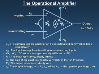
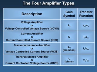
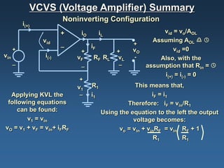
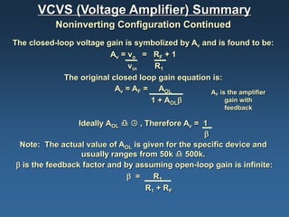
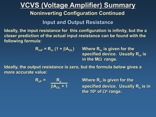
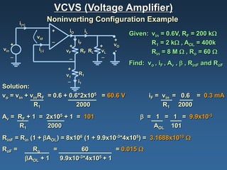
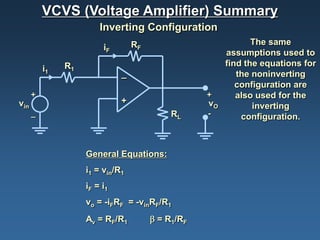
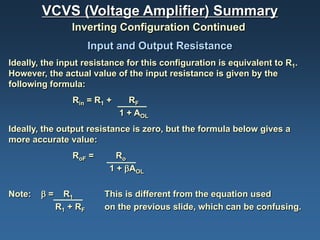
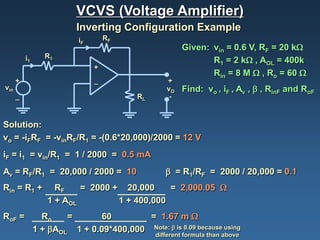
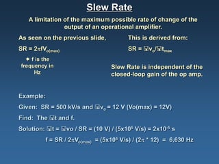
Operational Amplifiers


   Tutorial Series


       _


       +


                     Kristin Ackerson, Virginia Tech EE
                     Spring 2002 – VTech –Calvin Project
Table of Contents
The Operational Amplifier______________________________slides 3-4
The Four Amplifier Types______________________________slide 5
VCVS(Voltage Amplifier) Summary:
        Noninverting Configuration____________slides 6-9
        Inverting Configuration________________slides 10-12
ICIC(Current Amplifier) Summary________________________slide 13
VCIS (Transconductance Amplifier) Summary_____________slides 14-15
ICVS (Transresistance Amplifier) Summary_______________slides 16-18
Power Bandwidth_____________________________________slide 19
Slew Rate____________________________________________slide 20
Slew Rate Output Distortion____________________________ slide 21
Noise Gain___________________________________________slide 22
Gain-Bandwidth Product_______________________________slide 23
Cascaded Amplifiers - Bandwidth________________________slide 24
Common Mode Rejection Ratio__________________________slides 25-26
Power Supply Rejection Ratio___________________________slide 27
Sources_____________________________________________slide 28
The Operational Amplifier
•   Usually Called Op Amps
•   An amplifier is a device that accepts a varying input signal and
    produces a similar output signal with a larger amplitude.
•   Usually connected so part of the output is fed back to the input.
    (Feedback Loop)
•   Most Op Amps behave like voltage amplifiers. They take an input
    voltage and output a scaled version.
•   They are the basic components used to build analog circuits.
•   The name “operational amplifier” comes from the fact that they were
    originally used to perform mathematical operations such as
    integration and differentiation.
•   Integrated circuit fabrication techniques have made high-
    performance operational amplifiers very inexpensive in comparison
    to older discrete devices.
The Operational Amplifier
                                                    +VS

                       i(-)           _
        Inverting
                                                   RO
                                vid            A                      Output
                                          Ri
                                                                     vO = Advid
    Noninverting
                         i(+)         +

                                                        -VS
• i(+), i(-) : Currents into the amplifier on the inverting and noninverting lines
               respectively
• vid : The input voltage from inverting to non-inverting inputs
• +VS , -VS : DC source voltages, usually +15V and –15V
• Ri : The input resistance, ideally infinity
• A : The gain of the amplifier. Ideally very high, in the 1x10¹⁰ range.
• RO: The output resistance, ideally zero
• vO: The output voltage; vO = AOLvid where AOL is the open-loop voltage gain
The Four Amplifier Types
                                            Gain       Transfer
            Description                    Symbol      Function
            Voltage Amplifier
                    or                        Av         vo/vin
Voltage Controlled Voltage Source (VCVS)
           Current Amplifier
                   or                         Ai         io/iin
Current Controlled Current Source (ICIS)
      Transconductance Amplifier
                                               gm
                   or                                    io/vin
                                           (siemens)
Voltage Controlled Current Source (VCIS)
       Transresistance Amplifier
                                              rm
                   or                                    vo/iin
                                            (ohms)
Current Controlled Voltage Source (ICVS)
VCVS (Voltage Amplifier) Summary
                         Noninverting Configuration
          i(+)
                         +    iO        iL                   vid = vo/AOL
                 vid                                      Assuming AOL  
                         _         iF              +
      +                       +              +     vO            vid =0
vin               i(-)       vF     RF RL     vL   -        Also, with the
      _                                       _
                              _                         assumption that Rin = 
                                                             i(+) = i(-) = 0
                             +
                             v1    R1               This means that,
  Applying KVL the           _     i1                      iF = i 1
 following equations                             Therefore: iF = vin/R1
     can be found:                      Using the equation to the left the output
        v1 = vin                                   voltage becomes:
vO = v1 + vF = vin+ iFRF                      vo = vin + vinRF = vin RF + 1
                                                            R1       R1
VCVS (Voltage Amplifier) Summary
           Noninverting Configuration Continued
The closed-loop voltage gain is symbolized by Av and is found to be:
                         Av = vo = RF + 1
                               vin   R1
             The original closed loop gain equation is:
                           Av = AF = AOL           AF is the amplifier
                                    1 + AOLβ            gain with
                                                        feedback

                 Ideally AOL   , Therefore Av = 1
                                                  β
 Note: The actual value of AOL is given for the specific device and
                  usually ranges from 50k  500k.
β is the feedback factor and by assuming open-loop gain is infinite:
                              β =    R1
                                   R1 + RF
VCVS (Voltage Amplifier) Summary
             Noninverting Configuration Continued
                    Input and Output Resistance
Ideally, the input resistance for this configuration is infinity, but the a
closer prediction of the actual input resistance can be found with the
following formula:
                RinF = Rin (1 + βAOL)    Where Rin is given for the
                                         specified device. Usually Rin is
                                         in the MΩ range.
Ideally, the output resistance is zero, but the formula below gives a
more accurate value:
                RoF =     Ro             Where Ro is given for the
                        βAOL + 1         specified device. Usually Ro is in
                                         the 10s of Ωs range.
VCVS (Voltage Amplifier)
          i(+)
                         Noninverting Configuration Example
                          +    iO        iL
                 vid
                                                        Given: vin = 0.6V, RF = 200 kΩ
                          _         iF             +
      +                                            vO          R1 = 2 kΩ , AOL = 400k
                               +              +
vin               i(-)        vF     RF RL    vL   -           Rin = 8 M Ω , Ro = 60 Ω
      _                        _               _
                                                        Find: vo , iF , Av , β , RinF and RoF
                               +
                              v1    R1
                               _    i1
Solution:
vo = vin + vinRF = 0.6 + 0.6*2x105 = 60.6 V                    iF = vin = 0.6 = 0.3 mA
            R1              2000                                    R1 2000
Av = RF + 1 = 2x10⁵ + 1 = 101                               β = 1 = 1 = 9.9x10⁻³
     R1       2000                                              AOL 101
RinF = Rin (1 + βAOL) = 8x10⁶ (1 + 9.9x10-3*4x105) = 3.1688x10¹⁰ Ω
RoF =          Ro     =        60          = 0.015 Ω
             βAOL + 1   9.9x10-3*4x105 + 1
VCVS (Voltage Amplifier) Summary
                         Inverting Configuration
                                   RF                           The same
                          iF
                                                         assumptions used to
               R1                                        find the equations for
          i1
                               _                            the noninverting
                                                            configuration are
      +                                             +       also used for the
vin                            +                    vO          inverting
      _                                      RL     -        configuration.


                    General Equations:
                    i1 = vin/R1
                    iF = i 1
                    vo = -iFRF = -vinRF/R1
                    Av = RF/R1          β = R1/RF
VCVS (Voltage Amplifier) Summary
                Inverting Configuration Continued
                       Input and Output Resistance
Ideally, the input resistance for this configuration is equivalent to R1.
However, the actual value of the input resistance is given by the
following formula:
                 Rin = R1 +     RF
                              1 + AOL
Ideally, the output resistance is zero, but the formula below gives a
more accurate value:
                 RoF =       Ro
                           1 + βAOL

Note:   β=     R1         This is different from the equation used
             R1 + RF      on the previous slide, which can be confusing.
VCVS (Voltage Amplifier)
                          Inverting Configuration Example
                           iF       RF
                                                       Given: vin = 0.6 V, RF = 20 kΩ
          i1      R1
                                                              R1 = 2 kΩ , AOL = 400k
                                +
                                                              Rin = 8 M Ω , Ro = 60 Ω
      +                         _                 +
vin                                               vO   Find: vo , iF , Av , β , RinF and RoF
      _                                   RL       -


Solution:
vo = -iFRF = -vinRF/R1 = -(0.6*20,000)/2000 = 12 V
iF = i1 = vin/R1 = 1 / 2000 = 0.5 mA
Av = RF/R1 = 20,000 / 2000 = 10                   β = R1/RF = 2000 / 20,000 = 0.1
Rin = R1 +          RF    = 2000 + 20,000     = 2,000.05 Ω
                  1 + AOL         1 + 400,000
RoF =            Ro    =      60         = 1.67 m Ω
               1 + βAOL 1 + 0.09*400,000 Note: β is 0.09 because using
                                               different formula than above
ICIS (Current Amplifier) Summary
           Not commonly done using operational amplifiers
                  iL
                          Load
                      _
iin
                      +       iin = iL
                                                    Similar to the voltage
1 Possible                                         follower shown below:
   ICIS
Operational
 Amplifier                                                _
                                   +                              vin = vo
Application                  vin
                                   _                                +
                                                          +         vO
                                                                    -
Both these amplifiers have
        unity gain:
                                       Voltage Follower
        Av = Ai = 1
VCIS (Transconductance Amplifier) Summary
                        Voltage to Current Converter
                         iL                                                  iL
                              Load                                    Load
          i1   R1                                     i1   R1
                              _                                         _

      +                                OR         +
vin                           +             vin                         +
      _                                           _               +
                                                            vin
                                                                  _
 General Equations:
 iL = i1 = v1/R1
 v1 = vin
 The transconductance, gm = io/vin = 1/R1
 Therefore, iL = i1 = vin/R1 = gmvin
 The maximum load resistance is determined by:
 RL(max) = vo(max)/iL
VCIS (Transconductance Amplifier)
                     Voltage to Current Converter Example
                          iL
                               Load      Given: vin = 2 V, R1 = 2 kΩ
          i1    R1                              vo(max) =  10 V
                               _
                                         Find: iL , gm and RL(max)
      +
vin                            +
      _                               Solution:

                                      iL = i1 = vin/R1 = 2 / 2000 = 1 mA
Note:
                                      gm = io/vin = 1/R1 = 1 / 2000 = 0.5 mS
• If RL > RL(max) the op amp
  will saturate                       RL(max) = vo(max)/iL = 10 V / 1 mA
• The output current, iL is
  independent of the load                    = 10 k Ω
  resistance.
VCIS (Transresistance Amplifier) Summary
             Current to Voltage Converter
                              iF       RF


                                   _

                                            +
       iin                         +        vO
                                            -


               General Equations:
               iF = iin
               vo = -iFRF
               rm = vo/iin = RF
VCIS (Transresistance Amplifier) Summary
               Current to Voltage Converter

 •   Transresistance Amplifiers are used for low-power
     applications to produce an output voltage proportional to
     the input current.

 •   Photodiodes and Phototransistors, which are used in the
     production of solar power are commonly modeled as
     current sources.

 •   Current to Voltage Converters can be used to convert these
     current sources to more commonly used voltage sources.
VCIS (Transresistance Amplifier)
         Current to Voltage Converter Example
                  iF       RF
                                     Given: iin = 10 mA
                                             RF = 200 Ω
                       _
                                     Find: iF , vo and rm
                                +
iin                    +        vO
                                -


      Solution:

      iF = iin = 10 mA

      vo = -iFRF = 10 mA * 200 Ω = 2 V

      rm = vo/iin = RF = 200
Power Bandwidth
The maximum frequency at which a sinusoidal output signal can be
       produced without causing distortion in the signal.
  The power bandwidth, BWp is determined using the desired
 output signal amplitude and the the slew rate (see next slide)
                 specifications of the op amp.
                         BWp =      SR
                                 2πVo(max)
            SR = 2πfVo(max) where SR is the slew rate


Example:
Given: Vo(max) = 12 V and SR = 500 kV/s
Find:   BWp
Solution:       BWp =    500 kV/s = 6.63 kHz
                         2π * 12 V
Slew Rate
   A limitation of the maximum possible rate of change of the
                output of an operational amplifier.
As seen on the previous slide,         This is derived from:
SR = 2πfVo(max)                        SR = vo/tmax
   f is the
frequency in                     Slew Rate is independent of the
     Hz                          closed-loop gain of the op amp.


Example:
Given: SR = 500 kV/s and vo = 12 V (Vo(max) = 12V)
Find: The t and f.
Solution: t = vo / SR = (10 V) / (5x10⁵ V/s) = 2x10⁻⁵ s
         f = SR / 2πVo(max) = (5x10⁵ V/s) / (2π * 12) = 6,630 Hz
Slew Rate Distortion
  v
              desired output
                waveform           SR = v/t = m (slope)


                               
                               v                    t
                          
      actual output
                          t
       because of
        slew rate
        limitation


The picture above shows exactly what happens when the
 slew rate limitations are not met and the output of the
            operational amplifier is distorted.
Noise Gain
  The noise gain of an amplifier is independent of the amplifiers
            configuration (inverting or noninverting)
             The noise gain is given by the formula:
                           AN = R1 + RF
                                  R1

Example 1: Given a noninverting amplifier with the resistance
           values, R1 = 2 kΩ and RF = 200 kΩ
Find: The noise gain.
AN = 2 kΩ + 200 kΩ = 101              Note: For the
         2 kΩ                        noninverting amplifier AN = AV

Example 2: Given an inverting amplifier with the resistance
                   values, R1 = 2 kΩ and RF = 20 kΩ
Find: The noise gain.
AN = 2 kΩ + 20 kΩ = 12                Note: For the
         2 kΩ                        inverting amplifier AN > AV
Gain-Bandwidth Product
 In most operational amplifiers, the open-loop gain begins
dropping off at very low frequencies. Therefore, to make the
   op amp useful at higher frequencies, gain is traded for
                         bandwidth.
      The Gain-Bandwidth Product (GBW) is given by:
                       GBW = ANBW


Example: For a 741 op amp, a noise gain of 10 k corresponds
         to a bandwidth of ~200 Hz
Find: The GBW
       GBW = 10 k * 200 Hz = 2 MHz
Cascaded Amplifiers - Bandwidth
  Quite often, one amplifier does not increase the signal enough
 and amplifiers are cascaded so the output of one amplifier is the
                         input to the next.
The amplifiers are matched so:
BWS = BW1 = BW2 = GBW        where, BWS is the bandwidth of all
                   AN        the cascaded amplifiers and AN is
                             the noise gain
The Total Bandwidth of the Cascaded Amplifiers is:
BWT = BWs(21/n – 1)1/2       where n is the number of amplifiers
                             that are being cascaded
Example: Cascading 3 Amplifiers with GBW = 1 MHz and AN = 15,
Find: The Total Bandwidth, BWT
BWS = 1 MHz / 15 = 66.7 kHz
BWT = 66.7 kHz (21/3 – 1)1/2 = 34 kHz
Common-Mode Rejection Ratio
The common-mode rejection ratio (CMRR) relates to the ability of
 the op amp to reject common-mode input voltage. This is very
    important because common-mode signals are frequently
              encountered in op amp applications.
                     CMRR = 20 log|AN / Acm|
                       Acm =          AN
                              log-1 (CMRR / 20)
We solve for Acm because Op Amp data sheets list the CMRR value.

The common-mode input voltage is an average of the voltages that
  are present at the non-inverting and inverting terminals of the
                             amplifier.
                          vicm = v(+) + v(-)
                                      2
Common-Mode Rejection Ratio
                        Example

Given: A 741 op amp with CMRR = 90 dB and a noise gain,
       AN = 1 k
Find: The common mode gain, Acm


Acm =           AN        =      1000
        log-1 (CMRR / 20)     log-1 (90 / 20)

    = 0.0316

It is very desirable for the common-mode gain to be small.
Power Supply Rejection Ratio
One of the reasons op amps are so useful, is that they can
be operated from a wide variety of power supply voltages.

  The 741 op amp can be operated from bipolar supplies
ranging from 5V to 18V with out too many changes to
              the parameters of the op amp.

The power supply rejection ratio (SVRR) refers to the slight
  change in output voltage that occurs when the power
     supply of the op amp changes during operation.

                SVRR = 20 log (Vs / Vo)

 The SVRR value is given for a specified op amp. For the
 741 op amp, SVRR = 96 dB over the range 5V to 18V.
Open-Loop Op Amp Characteristics
                          Table 12.11


 Device      LM741C     LF351      OP-07     LH0003     AD549K

                                             Hybrid
Technology    BJT       BiFET       BJT                  BiFET
                                              BJT

 AOL(typ)     200 k     100 k       400 k     40 k        100 k

   Rin        2 MΩ      1012 Ω      8 MΩ     100 kΩ    1013 Ω || 1 pF


   Ro         50 Ω       30 Ω       60 Ω      50 Ω       ~100 Ω

   SR        0.5 V/µs   13 V/µs   0.3 V/µs   70 V/µs     3 V/µs

 CMRR         90 dB     100 dB     110 dB    90 dB        90 dB
Sources
Dailey, Denton. Electronic Devices and Circuits, Discrete and Integrated. Prentice Hall, New
          Jersey: 2001. (pp 456-509)
         1Table   12.1: Selected Op Amps and Their Open Loop Characteristics, pg 457
Liou, J.J. and Yuan, J.S. Semiconductor Device Physics and Simulation. Plenum Press,
           New York: 1998.
Neamen, Donald. Semiconductor Physics & Devices. Basic Principles. McGraw-Hill,
        Boston: 1997. (pp 351-357)


                                        Web Sources
                         www.infoplease.com/ce6/sci/A0803814.html
                       http://www.infoplease.com/ce6/sci/A0836717.html
                     http://people.msoe.edu/~saadat/PSpice230Part3.htm

Op amp tutorial-1

  • 1.
    Operational Amplifiers Tutorial Series _ + Kristin Ackerson, Virginia Tech EE Spring 2002 – VTech –Calvin Project
  • 2.
    Table of Contents TheOperational Amplifier______________________________slides 3-4 The Four Amplifier Types______________________________slide 5 VCVS(Voltage Amplifier) Summary: Noninverting Configuration____________slides 6-9 Inverting Configuration________________slides 10-12 ICIC(Current Amplifier) Summary________________________slide 13 VCIS (Transconductance Amplifier) Summary_____________slides 14-15 ICVS (Transresistance Amplifier) Summary_______________slides 16-18 Power Bandwidth_____________________________________slide 19 Slew Rate____________________________________________slide 20 Slew Rate Output Distortion____________________________ slide 21 Noise Gain___________________________________________slide 22 Gain-Bandwidth Product_______________________________slide 23 Cascaded Amplifiers - Bandwidth________________________slide 24 Common Mode Rejection Ratio__________________________slides 25-26 Power Supply Rejection Ratio___________________________slide 27 Sources_____________________________________________slide 28
  • 3.
    The Operational Amplifier • Usually Called Op Amps • An amplifier is a device that accepts a varying input signal and produces a similar output signal with a larger amplitude. • Usually connected so part of the output is fed back to the input. (Feedback Loop) • Most Op Amps behave like voltage amplifiers. They take an input voltage and output a scaled version. • They are the basic components used to build analog circuits. • The name “operational amplifier” comes from the fact that they were originally used to perform mathematical operations such as integration and differentiation. • Integrated circuit fabrication techniques have made high- performance operational amplifiers very inexpensive in comparison to older discrete devices.
  • 4.
    The Operational Amplifier +VS i(-) _ Inverting RO vid A Output Ri vO = Advid Noninverting i(+) + -VS • i(+), i(-) : Currents into the amplifier on the inverting and noninverting lines respectively • vid : The input voltage from inverting to non-inverting inputs • +VS , -VS : DC source voltages, usually +15V and –15V • Ri : The input resistance, ideally infinity • A : The gain of the amplifier. Ideally very high, in the 1x10¹⁰ range. • RO: The output resistance, ideally zero • vO: The output voltage; vO = AOLvid where AOL is the open-loop voltage gain
  • 5.
    The Four AmplifierTypes Gain Transfer Description Symbol Function Voltage Amplifier or Av vo/vin Voltage Controlled Voltage Source (VCVS) Current Amplifier or Ai io/iin Current Controlled Current Source (ICIS) Transconductance Amplifier gm or io/vin (siemens) Voltage Controlled Current Source (VCIS) Transresistance Amplifier rm or vo/iin (ohms) Current Controlled Voltage Source (ICVS)
  • 6.
    VCVS (Voltage Amplifier)Summary Noninverting Configuration i(+) + iO iL vid = vo/AOL vid Assuming AOL   _ iF + + + + vO vid =0 vin i(-) vF RF RL vL - Also, with the _ _ _ assumption that Rin =  i(+) = i(-) = 0 + v1 R1 This means that, Applying KVL the _ i1 iF = i 1 following equations Therefore: iF = vin/R1 can be found: Using the equation to the left the output v1 = vin voltage becomes: vO = v1 + vF = vin+ iFRF vo = vin + vinRF = vin RF + 1 R1 R1
  • 7.
    VCVS (Voltage Amplifier)Summary Noninverting Configuration Continued The closed-loop voltage gain is symbolized by Av and is found to be: Av = vo = RF + 1 vin R1 The original closed loop gain equation is: Av = AF = AOL AF is the amplifier 1 + AOLβ gain with feedback Ideally AOL   , Therefore Av = 1 β Note: The actual value of AOL is given for the specific device and usually ranges from 50k  500k. β is the feedback factor and by assuming open-loop gain is infinite: β = R1 R1 + RF
  • 8.
    VCVS (Voltage Amplifier)Summary Noninverting Configuration Continued Input and Output Resistance Ideally, the input resistance for this configuration is infinity, but the a closer prediction of the actual input resistance can be found with the following formula: RinF = Rin (1 + βAOL) Where Rin is given for the specified device. Usually Rin is in the MΩ range. Ideally, the output resistance is zero, but the formula below gives a more accurate value: RoF = Ro Where Ro is given for the βAOL + 1 specified device. Usually Ro is in the 10s of Ωs range.
  • 9.
    VCVS (Voltage Amplifier) i(+) Noninverting Configuration Example + iO iL vid Given: vin = 0.6V, RF = 200 kΩ _ iF + + vO R1 = 2 kΩ , AOL = 400k + + vin i(-) vF RF RL vL - Rin = 8 M Ω , Ro = 60 Ω _ _ _ Find: vo , iF , Av , β , RinF and RoF + v1 R1 _ i1 Solution: vo = vin + vinRF = 0.6 + 0.6*2x105 = 60.6 V iF = vin = 0.6 = 0.3 mA R1 2000 R1 2000 Av = RF + 1 = 2x10⁵ + 1 = 101 β = 1 = 1 = 9.9x10⁻³ R1 2000 AOL 101 RinF = Rin (1 + βAOL) = 8x10⁶ (1 + 9.9x10-3*4x105) = 3.1688x10¹⁰ Ω RoF = Ro = 60 = 0.015 Ω βAOL + 1 9.9x10-3*4x105 + 1
  • 10.
    VCVS (Voltage Amplifier)Summary Inverting Configuration RF The same iF assumptions used to R1 find the equations for i1 _ the noninverting configuration are + + also used for the vin + vO inverting _ RL - configuration. General Equations: i1 = vin/R1 iF = i 1 vo = -iFRF = -vinRF/R1 Av = RF/R1 β = R1/RF
  • 11.
    VCVS (Voltage Amplifier)Summary Inverting Configuration Continued Input and Output Resistance Ideally, the input resistance for this configuration is equivalent to R1. However, the actual value of the input resistance is given by the following formula: Rin = R1 + RF 1 + AOL Ideally, the output resistance is zero, but the formula below gives a more accurate value: RoF = Ro 1 + βAOL Note: β= R1 This is different from the equation used R1 + RF on the previous slide, which can be confusing.
  • 12.
    VCVS (Voltage Amplifier) Inverting Configuration Example iF RF Given: vin = 0.6 V, RF = 20 kΩ i1 R1 R1 = 2 kΩ , AOL = 400k + Rin = 8 M Ω , Ro = 60 Ω + _ + vin vO Find: vo , iF , Av , β , RinF and RoF _ RL - Solution: vo = -iFRF = -vinRF/R1 = -(0.6*20,000)/2000 = 12 V iF = i1 = vin/R1 = 1 / 2000 = 0.5 mA Av = RF/R1 = 20,000 / 2000 = 10 β = R1/RF = 2000 / 20,000 = 0.1 Rin = R1 + RF = 2000 + 20,000 = 2,000.05 Ω 1 + AOL 1 + 400,000 RoF = Ro = 60 = 1.67 m Ω 1 + βAOL 1 + 0.09*400,000 Note: β is 0.09 because using different formula than above
  • 13.
    ICIS (Current Amplifier)Summary  Not commonly done using operational amplifiers iL Load _ iin + iin = iL Similar to the voltage 1 Possible follower shown below: ICIS Operational Amplifier _ + vin = vo Application vin _ + + vO - Both these amplifiers have unity gain: Voltage Follower Av = Ai = 1
  • 14.
    VCIS (Transconductance Amplifier)Summary Voltage to Current Converter iL iL Load Load i1 R1 i1 R1 _ _ + OR + vin + vin + _ _ + vin _ General Equations: iL = i1 = v1/R1 v1 = vin The transconductance, gm = io/vin = 1/R1 Therefore, iL = i1 = vin/R1 = gmvin The maximum load resistance is determined by: RL(max) = vo(max)/iL
  • 15.
    VCIS (Transconductance Amplifier) Voltage to Current Converter Example iL Load Given: vin = 2 V, R1 = 2 kΩ i1 R1 vo(max) =  10 V _ Find: iL , gm and RL(max) + vin + _ Solution: iL = i1 = vin/R1 = 2 / 2000 = 1 mA Note: gm = io/vin = 1/R1 = 1 / 2000 = 0.5 mS • If RL > RL(max) the op amp will saturate RL(max) = vo(max)/iL = 10 V / 1 mA • The output current, iL is independent of the load = 10 k Ω resistance.
  • 16.
    VCIS (Transresistance Amplifier)Summary Current to Voltage Converter iF RF _ + iin + vO - General Equations: iF = iin vo = -iFRF rm = vo/iin = RF
  • 17.
    VCIS (Transresistance Amplifier)Summary Current to Voltage Converter • Transresistance Amplifiers are used for low-power applications to produce an output voltage proportional to the input current. • Photodiodes and Phototransistors, which are used in the production of solar power are commonly modeled as current sources. • Current to Voltage Converters can be used to convert these current sources to more commonly used voltage sources.
  • 18.
    VCIS (Transresistance Amplifier) Current to Voltage Converter Example iF RF Given: iin = 10 mA RF = 200 Ω _ Find: iF , vo and rm + iin + vO - Solution: iF = iin = 10 mA vo = -iFRF = 10 mA * 200 Ω = 2 V rm = vo/iin = RF = 200
  • 19.
    Power Bandwidth The maximumfrequency at which a sinusoidal output signal can be produced without causing distortion in the signal. The power bandwidth, BWp is determined using the desired output signal amplitude and the the slew rate (see next slide) specifications of the op amp. BWp = SR 2πVo(max) SR = 2πfVo(max) where SR is the slew rate Example: Given: Vo(max) = 12 V and SR = 500 kV/s Find: BWp Solution: BWp = 500 kV/s = 6.63 kHz 2π * 12 V
  • 20.
    Slew Rate A limitation of the maximum possible rate of change of the output of an operational amplifier. As seen on the previous slide, This is derived from: SR = 2πfVo(max) SR = vo/tmax  f is the frequency in Slew Rate is independent of the Hz closed-loop gain of the op amp. Example: Given: SR = 500 kV/s and vo = 12 V (Vo(max) = 12V) Find: The t and f. Solution: t = vo / SR = (10 V) / (5x10⁵ V/s) = 2x10⁻⁵ s f = SR / 2πVo(max) = (5x10⁵ V/s) / (2π * 12) = 6,630 Hz
  • 21.
    Slew Rate Distortion v desired output waveform SR = v/t = m (slope)  v t  actual output t because of slew rate limitation The picture above shows exactly what happens when the slew rate limitations are not met and the output of the operational amplifier is distorted.
  • 22.
    Noise Gain The noise gain of an amplifier is independent of the amplifiers configuration (inverting or noninverting) The noise gain is given by the formula: AN = R1 + RF R1 Example 1: Given a noninverting amplifier with the resistance values, R1 = 2 kΩ and RF = 200 kΩ Find: The noise gain. AN = 2 kΩ + 200 kΩ = 101  Note: For the 2 kΩ noninverting amplifier AN = AV Example 2: Given an inverting amplifier with the resistance values, R1 = 2 kΩ and RF = 20 kΩ Find: The noise gain. AN = 2 kΩ + 20 kΩ = 12  Note: For the 2 kΩ inverting amplifier AN > AV
  • 23.
    Gain-Bandwidth Product Inmost operational amplifiers, the open-loop gain begins dropping off at very low frequencies. Therefore, to make the op amp useful at higher frequencies, gain is traded for bandwidth. The Gain-Bandwidth Product (GBW) is given by: GBW = ANBW Example: For a 741 op amp, a noise gain of 10 k corresponds to a bandwidth of ~200 Hz Find: The GBW GBW = 10 k * 200 Hz = 2 MHz
  • 24.
    Cascaded Amplifiers -Bandwidth Quite often, one amplifier does not increase the signal enough and amplifiers are cascaded so the output of one amplifier is the input to the next. The amplifiers are matched so: BWS = BW1 = BW2 = GBW where, BWS is the bandwidth of all AN the cascaded amplifiers and AN is the noise gain The Total Bandwidth of the Cascaded Amplifiers is: BWT = BWs(21/n – 1)1/2 where n is the number of amplifiers that are being cascaded Example: Cascading 3 Amplifiers with GBW = 1 MHz and AN = 15, Find: The Total Bandwidth, BWT BWS = 1 MHz / 15 = 66.7 kHz BWT = 66.7 kHz (21/3 – 1)1/2 = 34 kHz
  • 25.
    Common-Mode Rejection Ratio Thecommon-mode rejection ratio (CMRR) relates to the ability of the op amp to reject common-mode input voltage. This is very important because common-mode signals are frequently encountered in op amp applications. CMRR = 20 log|AN / Acm| Acm = AN log-1 (CMRR / 20) We solve for Acm because Op Amp data sheets list the CMRR value. The common-mode input voltage is an average of the voltages that are present at the non-inverting and inverting terminals of the amplifier. vicm = v(+) + v(-) 2
  • 26.
    Common-Mode Rejection Ratio Example Given: A 741 op amp with CMRR = 90 dB and a noise gain, AN = 1 k Find: The common mode gain, Acm Acm = AN = 1000 log-1 (CMRR / 20) log-1 (90 / 20) = 0.0316 It is very desirable for the common-mode gain to be small.
  • 27.
    Power Supply RejectionRatio One of the reasons op amps are so useful, is that they can be operated from a wide variety of power supply voltages. The 741 op amp can be operated from bipolar supplies ranging from 5V to 18V with out too many changes to the parameters of the op amp. The power supply rejection ratio (SVRR) refers to the slight change in output voltage that occurs when the power supply of the op amp changes during operation. SVRR = 20 log (Vs / Vo) The SVRR value is given for a specified op amp. For the 741 op amp, SVRR = 96 dB over the range 5V to 18V.
  • 28.
    Open-Loop Op AmpCharacteristics Table 12.11 Device LM741C LF351 OP-07 LH0003 AD549K Hybrid Technology BJT BiFET BJT BiFET BJT AOL(typ) 200 k 100 k 400 k 40 k 100 k Rin 2 MΩ 1012 Ω 8 MΩ 100 kΩ 1013 Ω || 1 pF Ro 50 Ω 30 Ω 60 Ω 50 Ω ~100 Ω SR 0.5 V/µs 13 V/µs 0.3 V/µs 70 V/µs 3 V/µs CMRR 90 dB 100 dB 110 dB 90 dB 90 dB
  • 29.
    Sources Dailey, Denton. ElectronicDevices and Circuits, Discrete and Integrated. Prentice Hall, New Jersey: 2001. (pp 456-509) 1Table 12.1: Selected Op Amps and Their Open Loop Characteristics, pg 457 Liou, J.J. and Yuan, J.S. Semiconductor Device Physics and Simulation. Plenum Press, New York: 1998. Neamen, Donald. Semiconductor Physics & Devices. Basic Principles. McGraw-Hill, Boston: 1997. (pp 351-357) Web Sources www.infoplease.com/ce6/sci/A0803814.html http://www.infoplease.com/ce6/sci/A0836717.html http://people.msoe.edu/~saadat/PSpice230Part3.htm