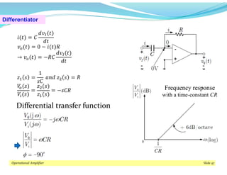
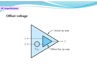
This document discusses operational amplifiers (op-amps), outlining their definitions, configurations, and ideal characteristics. Op-amps serve as fundamental components in various electronic circuits, demonstrating significant application in both analog computers and modern devices. The content further elaborates on inverting and non-inverting configurations, gain specifications, and imperfections such as offset voltage and input bias currents.

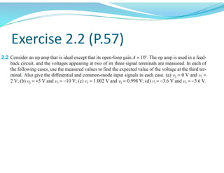


![Example 2.5 (P.85)
Find the output produced by a Miller integrator in response to an
input pulse of 1-V height and 1-ms width [below figure]. Let
R10kand C 10nF. The op amp is specified to saturate at
± 13𝑉.](https://image.slidesharecdn.com/chapter1-241116141053-7f192852/85/Chapter1-analog-electric-op-amp-and-application-46-320.jpg)