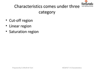
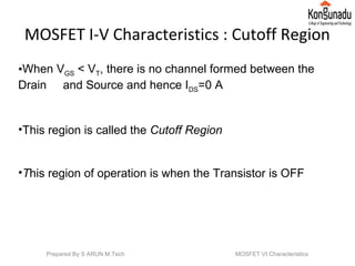
The document discusses the I-V characteristics of MOSFETs, which occur in three regions: cutoff, linear, and saturation. In cutoff region (VGS < VT), no channel is formed and IDS = 0. In linear region (VGS > VT, VDS < VGS - VT), IDS varies linearly with VDS. In saturation region (VGS > VT, VDS > VGS - VT), further increases in VDS do not increase IDS due to channel pinch-off. Equations are provided to describe IDS in each region.


![• The Drain to Source current (IDS) is given by the
expression:
• Where:
un = electron surface mobility (units in cm2
/V·s)
Cox = Unit Oxide Capacitance (units in F/cm2
)
W = width of the gate
L = length of the gate
• Remember this expression is only valid when :
VGS>VT
0 < VDS < VDSAT
( )[ ]2
02
2
DSDSTGS
oxn
DS VVVV
L
WCu
I linear
−⋅−⋅⋅⋅
⋅
=
Prepared By S ARUN M.Tech MOSFET VI Characteristics](https://image.slidesharecdn.com/mosfet-181127115058/85/Mosfet-8-320.jpg)
![• what is linear about this equation?
• Most of the parameters are constants during evaluation.
They are sometimes lumped into single parameters
• Notice that W and L are parameters that the designers have
control over. Most of the other parameters are defined by
the fabrication process and are out of the control of the IC
designer.
( )[ ]2
02
2
DSDSTGS
oxn
DS VVVV
L
WCu
I linear
−⋅−⋅⋅⋅
⋅
=
oxn Cuk ⋅=' ( )[ ]2
02
2
'
DSDSTGSDS VVVV
L
Wk
I linear
−⋅−⋅⋅⋅=
L
W
Cuk oxn ⋅⋅= ( )[ ]2
02
2
DSDSTGSDS VVVV
k
I linear
−⋅−⋅⋅=
Prepared By S ARUN M.Tech MOSFET VI Characteristics](https://image.slidesharecdn.com/mosfet-181127115058/85/Mosfet-9-320.jpg)
![• What is linear about this equation?
• The -VDS
2
term alters the function shape in the linear region.
As it becomes large enough to significantly decrease IDSin
this function, the transistor enters saturation and this
expression is no longer valid.
( )[ ]2
02
2
DSDSTGSDS VVVV
k
I linear
−⋅−⋅⋅=
For a fixed VGS,
then
IDS depends on
VDS
VDS
2
has a smaller effect on
IDS at low values of VDS
since it is not multiplied by
anything
Prepared By S ARUN M.Tech MOSFET VI Characteristics](https://image.slidesharecdn.com/mosfet-181127115058/85/Mosfet-10-320.jpg)
![• Since we know what the current will not decrease as VDS
increases past VDSAT, we can usethis expression to define VDSAT
• when VDS>(VGS-VT), then IDS in this expression begins to decrease
• we can then define VDSAT = (VGS-VT)
• So now we have the formal limits on the linear region and the validity of
this expression:
•
Linear Region : VGS>VT
0 < VDS < (VGS-VT)
( )[ ]2
02
2
DSDSTGSDS VVVV
k
I linear
−⋅−⋅⋅=
Prepared By S ARUN M.Tech MOSFET VI Characteristics](https://image.slidesharecdn.com/mosfet-181127115058/85/Mosfet-11-320.jpg)
![MOSFET I-V Characteristics : Saturation Region
• MOSFET is defined as being in saturation when:
Saturation Region : VGS> VT and VDS > (VGS-VT)
• An increase in VDS does not increase IDS because the channel is pinched-off
• However, an increase in VGS DOES increase IDSby increasing the channel
depth and hence the amount of current that can be conducted.
• Measurements on MOSFETS have shown that the dependence of IDS on VGS
tends to remain approximately constant around the peak value reached
for VDS=VDSAT
• A substitution of VDS=(VGS-VT0) yields:
( ) ( ) ( )[ ]
( )2
0
2
000
2
2
2
TGSDS
TGSTGSTGSDS
VV
k
I
VVVVVV
k
I
sat
sat
−⋅=
−−−⋅−⋅⋅=
Prepared By S ARUN M.Tech MOSFET VI Characteristics](https://image.slidesharecdn.com/mosfet-181127115058/85/Mosfet-12-320.jpg)
![1st order expressions for all three
regions of operation for the MOSFET
Now we have
Region Conditions IDS
Cutoff VGS< VT
Linear VGS> VT
VDS < (VGS-VT)
Saturation VGS> VT
VDS > (VGS-VT)
0=cutoffDSI
( )2
0
2
TGSDS VV
k
I sat
−⋅=
( )[ ]2
02
2
DSDSTGSDS VVVV
k
I linear
−⋅−⋅⋅=
Prepared By S ARUN M.Tech MOSFET VI Characteristics](https://image.slidesharecdn.com/mosfet-181127115058/85/Mosfet-13-320.jpg)