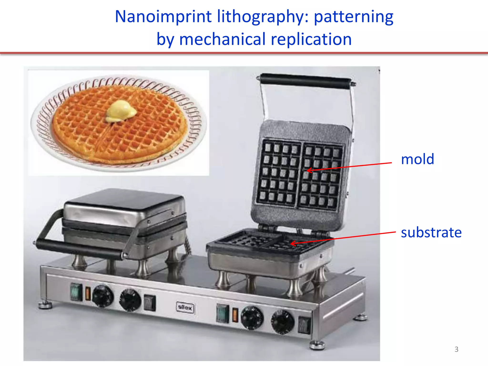
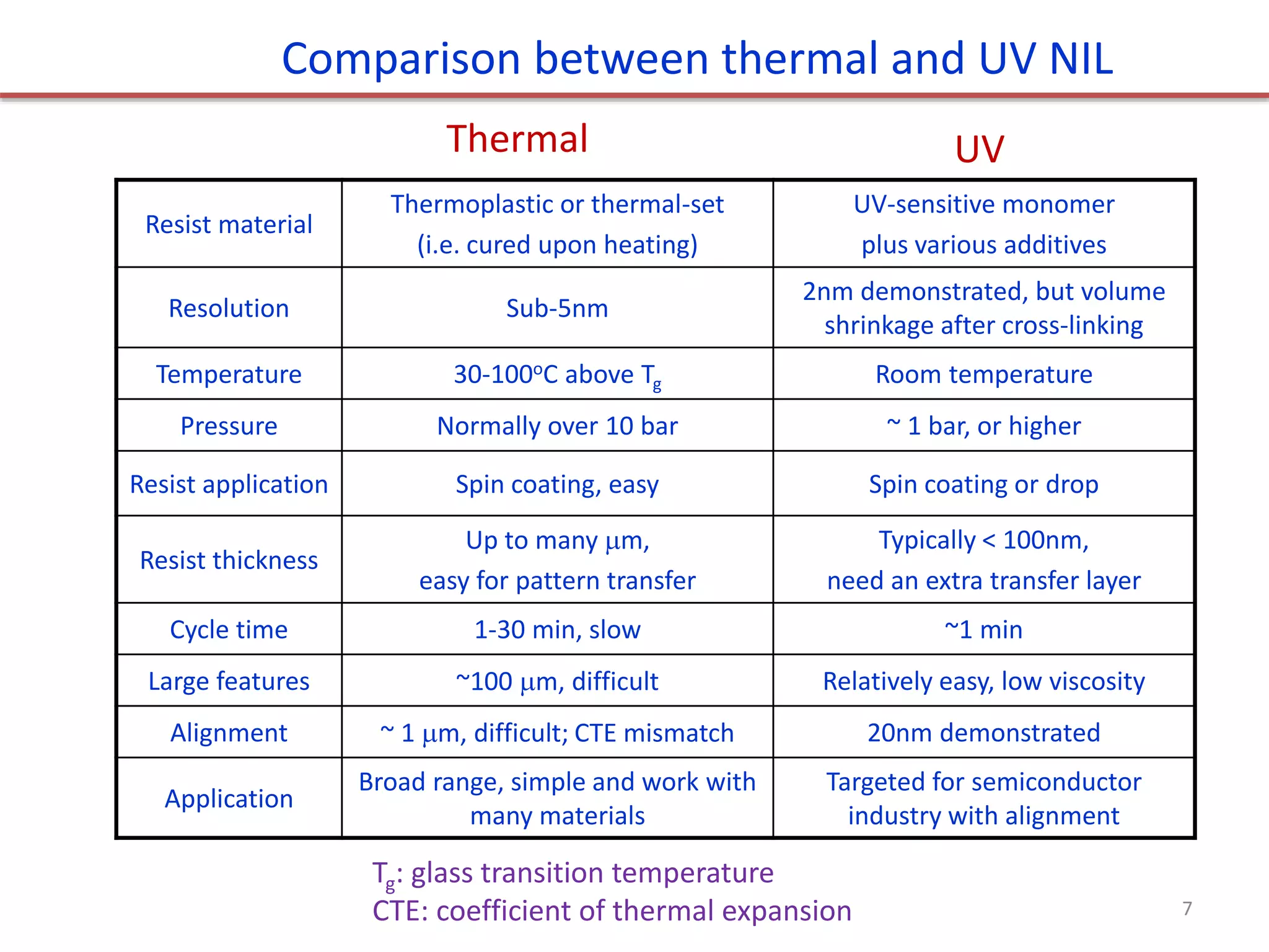
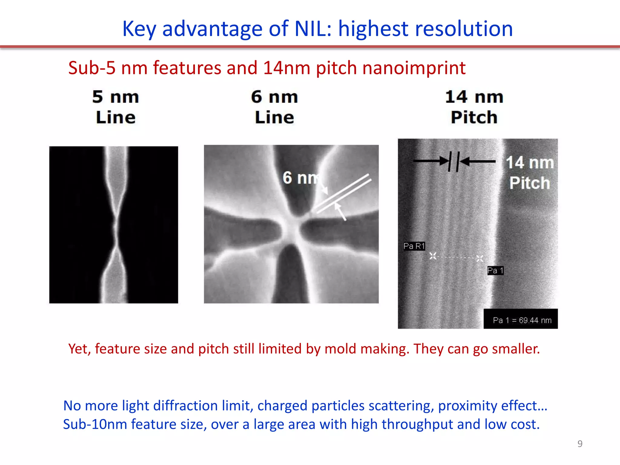
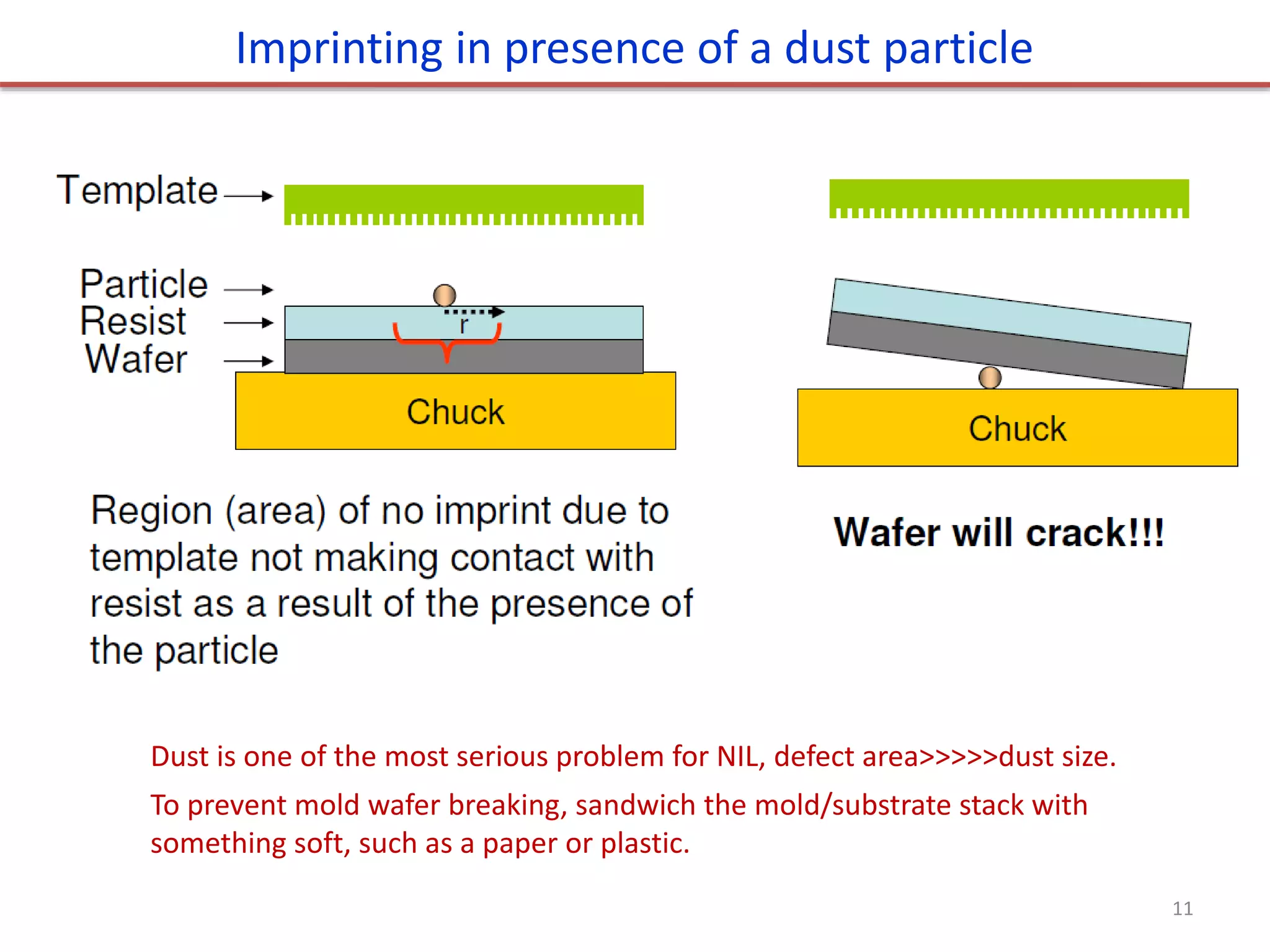
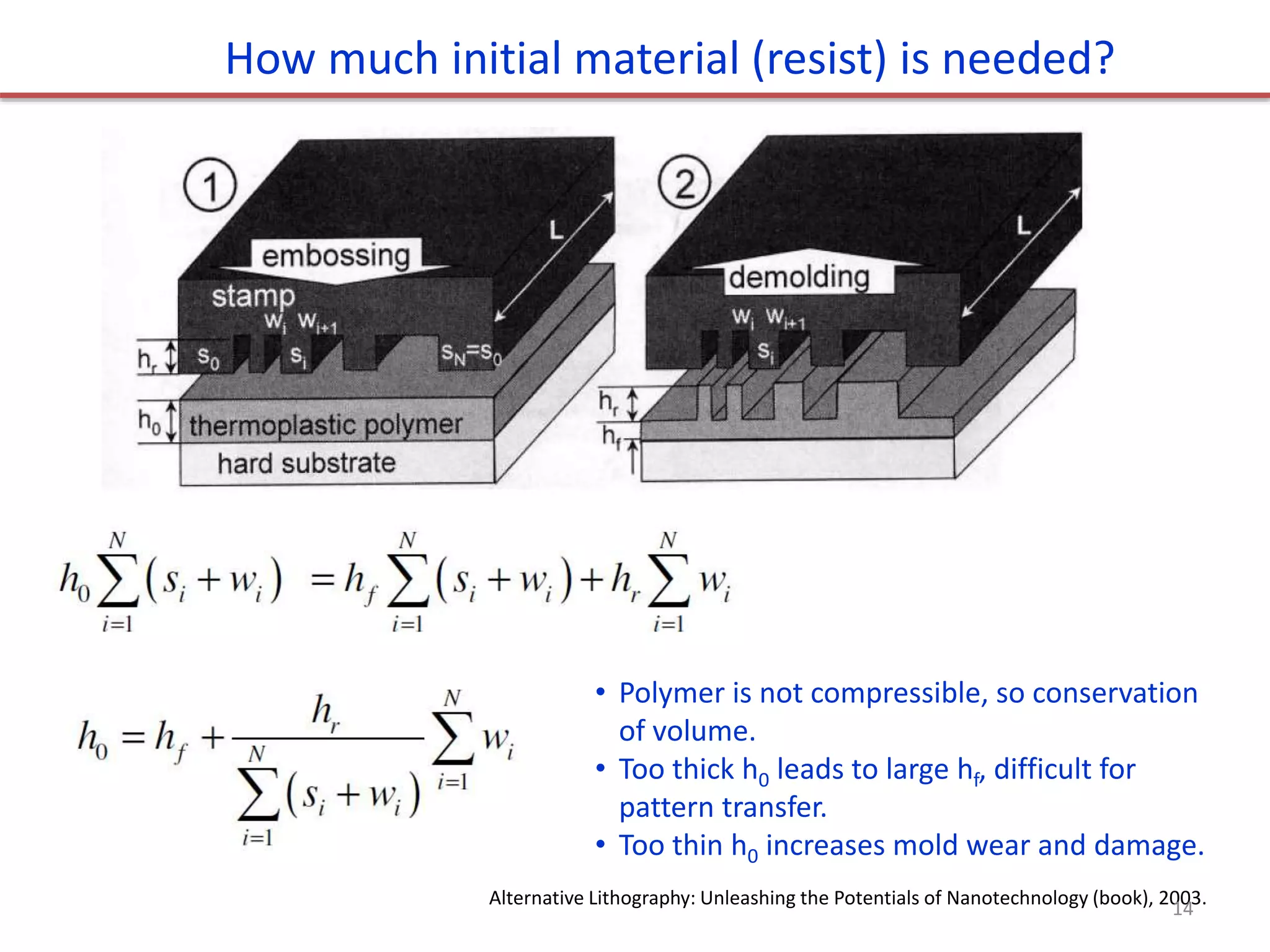
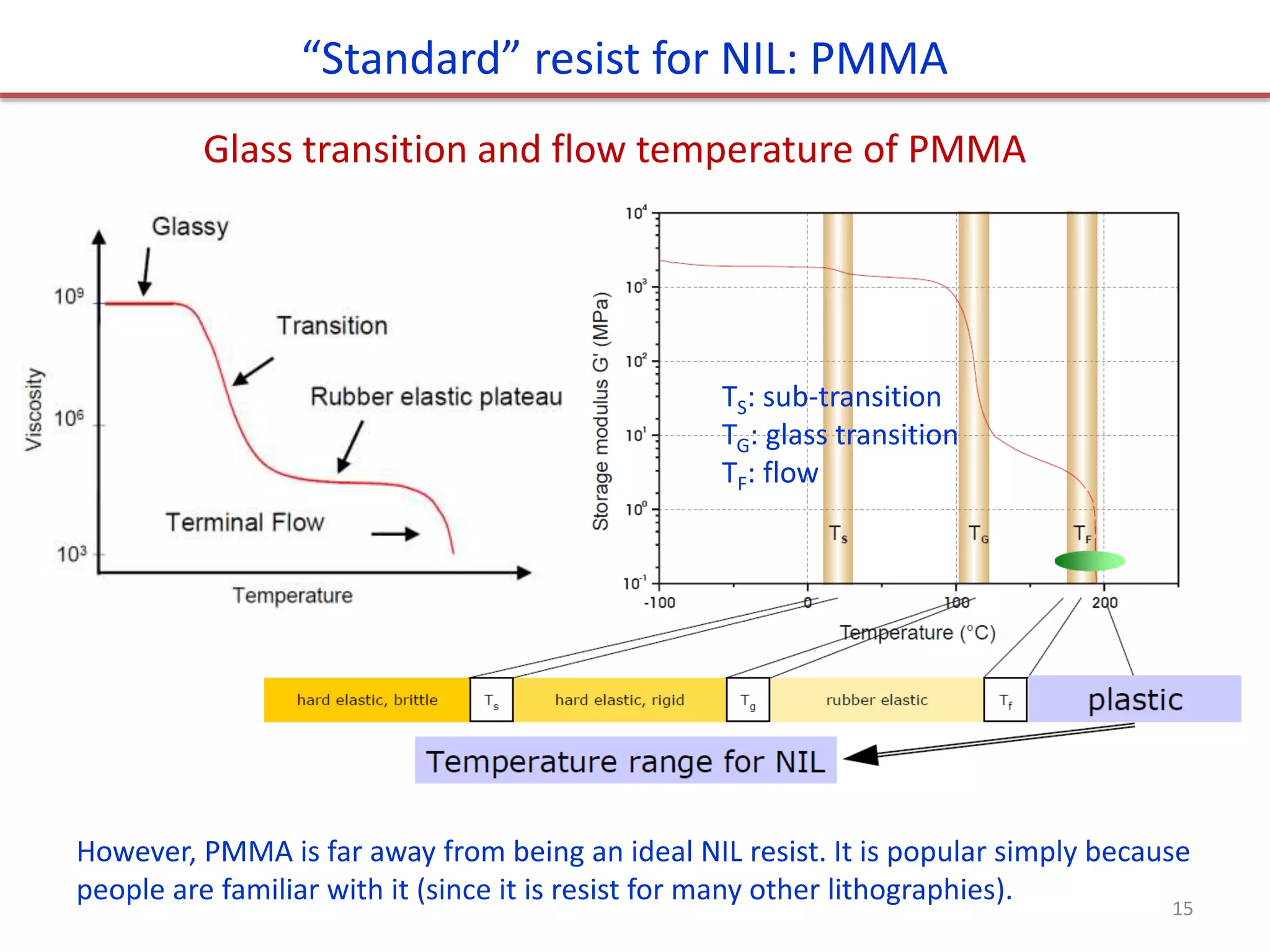
Nanoimprint Lithography head points:
Approaches: thermal and UV NIL
Properties of NIL
Overview. of NIL
Thermal NIL resists.
Residual layer after NIL.
NIL for large features (more difficult than small one).
Room temperature NIL, reverse NIL, inking.
NIL of bulk resist (polymer sheet, pellets).
https://www.linkedin.com/in/preeti-choudhary-266414182/
https://www.instagram.com/chaudharypreeti1997/
https://www.facebook.com/profile.php?id=100013419194533
https://twitter.com/preetic27018281
Please like, share, comment and follow.
stay connected
If any query then contact:
chaudharypreeti1997@gmail.com
Thanking-You
Preeti Choudhary
Different types of Nanolithography technique.
Types: Electron beam lithography, Photolithography, electron-beam writing, ion- lithography, X-ray lithography, and related images, concepts and graphical views.
I hope this presentation helpful for you.
https://www.linkedin.com/in/preeti-choudhary-266414182/
https://www.instagram.com/chaudharypreeti1997/
https://www.facebook.com/profile.php?id=100013419194533
https://twitter.com/preetic27018281
Please like, share, comment and follow.
stay connected
If any query then contact:
chaudharypreeti1997@gmail.com
Thanking-You
Preeti Choudhary
Lithography is the process of transferring patterns of geometric shapes in a mask to a radiation sensitive material called resist,which cover the surface of semiconductor wafer.
Hot wall reactor is a high temperature chamber in which the substrate is placed for coating. In this reactor including the substrate, all other parts (inlet and outlet tubes) inside the chamber get coated.
Chemical Vapour Deposition is a Chemical Synthesis route of Nanomaterials. Specially thin films like Graphene and Carbon NanoTubes are grown by this method.
This presentation includes basis of lithography i.e. (photo-lithography e-beam lithography) in nano-lithography includes (AFM, Soft, NIL and DPN lithography)
Novel effects can occur in materials when structures are formed with sizes comparable to any one of many possible length scales, such as the de Broglie wavelength of electrons, or the optical wavelengths of high energy photons. In these cases quantum mechanical effects can dominate material properties. One example is quantum confinement where the electronic properties of solids are altered with great reductions in particle size. The optical properties of nanoparticles, e.g. fluorescence, also become a function of the particle diameter. This effect does not come into play by going from macrosocopic to micrometer dimensions, but becomes pronounced when the nanometer scale is reached.
Discusses about photolithography, mask design, wet and dry bulk etching, bonding, thin film deposition and removal, metallization, sacrificial process and other inorganic processes.
Discusses about biomedical microdevices, systems and its various applications such as miniaturized systems including microelectronics, MEMS, microfluidics and nanosystmes measured in microns and nanometers.
Lithographic photomasks are typically transparent fused silica blanks covered with a pattern defined with a chrome metal-absorbing film. Photomasks are used at wavelengths of 365 nm, 248 nm, and 193 nm. Photomasks have also been developed for other forms of radiation such as 157 nm, 13.5 nm (EUV), X-ray, electrons, and ions; but these require entirely new materials for the substrate and the pattern film.
Rosa alejandra lukaszew a review of the thin film techniques potentially ap...thinfilmsworkshop
SRF is a surface phenomenon where only ~10 penetration depths are needed (l=40 nm for niobium), thus it has been recognized for some time now that it would be economically convenient to use thin film coated cavities. But problems arise with defects within 1 or 2 l of the surface or on the surface, and insufficient attention has been paid to this topic, including trapping of impurities like oxygen in defects as well as surface roughness enabling magnetic field pinning sites. Earlier attempts at CERN applied standard sputter PVD methods, but the grain size for the CERN Nb/Cu films was 100 nm, which is 10,000 times smaller than for conventional SRF cavities with the ensuing problems that appear at grain boundaries. Thus, these prior attempts showed higher surface resistance and worst Q-slope than bulk. I will review more modern approaches using higher energetic PVD methods for thin film deposition which offer promise to achieve thin films with improved superconducting performance.
Discusses about Microsystems Technologies ,Micro Stereolithography.Basic concepts and terminology such as Selected traditional micromachining photolithography and mask design, wet and dry bulk etching, bonding, thin film deposition and removal, metallization, sacrificial processes, other inorganic processes, electroplating
High performance liquid chromatography (HPLC) head points:
HPLC Advantages Vs GC
Instrumentation
HPLC System
Separations
Mobile Phase Reservoirs
Degasser
Aim of Gradient system
High/Low pressure gradient system
HPLC Pump Criteria
HPLC Pumps: Types
Reciprocating Pumps
Sample introduction
Manual Injector
Auto Injector
HPLC Modes
The Mobile Phase
Hydrophobic interaction
Common reverse phase solvents
Detectors
https://www.linkedin.com/in/preeti-choudhary-266414182/
https://www.instagram.com/chaudharypreeti1997/
https://www.facebook.com/profile.php?id=100013419194533
https://twitter.com/preetic27018281
Please like, share, comment and follow.
stay connected
If any query then contact:
chaudharypreeti1997@gmail.com
Thanking-You
Preeti Choudhary
Gas chromatography head points:
Invention of Chromatography
original chromatography Experiment
Common types of chromatography
Paper and Thin layer chromatography
How does chromatography work?
Theoretical Plate
gas chromatography
schematic of GC
carrier gas-supply
Injection port
sample Injection system
split/spitless Injection
sample valves
GC columns
open tubular columns
Temperature Control
Solid Support Materials
Particle size of Supports
The stationary Phase
Detection systems
Characteristics of the Ideal Detector
Flame Ionization Detectors
Thermal Conductivity Detector
Electron-capture Detectors
https://www.linkedin.com/in/preeti-choudhary-266414182/
https://www.instagram.com/chaudharypreeti1997/
https://www.facebook.com/profile.php?id=100013419194533
https://twitter.com/preetic27018281
Please like, share, comment and follow.
stay connected
If any query then contact:
chaudharypreeti1997@gmail.com
Thanking-You
Preeti Choudhary
Theory and Principle of FTIR head points:
What is Infrared Region?
Infrared Spectroscopy
What is FTIR?
Superiority of FTIR
FTIR optical system diagram
sampling techniques
The sample analysis process
advantage of FTIR
References
https://www.linkedin.com/in/preeti-choudhary-266414182/
https://www.instagram.com/chaudharypreeti1997/
https://www.facebook.com/profile.php?id=100013419194533
https://twitter.com/preetic27018281
Please like, share, comment and follow.
stay connected
If any query then contact:
chaudharypreeti1997@gmail.com
Thanking-You
Preeti Choudhary
Scanning Probe microscopy (AFM and STM) head point
AFM: Configuration of AFM
Parts of AFM system and Principle of AFM
Three Modes of AFM
AFM Instrument
Advantage and disadvantage
STM
Schematic Diagram
AFM and STM
https://www.linkedin.com/in/preeti-choudhary-266414182/
https://www.instagram.com/chaudharypreeti1997/
https://www.facebook.com/profile.php?id=100013419194533
https://twitter.com/preetic27018281
Please like, share, comment and follow.
stay connected
If any query then contact:
chaudharypreeti1997@gmail.com
Thanking-You
Preeti Choudhary
X-Ray Diffraction head points:
Introduction
History
How Diffraction Works
Demonstration
Analyzing Diffraction Patterns
Solving DNA
Applications
Summary and Conclusions
https://www.linkedin.com/in/preeti-choudhary-266414182/
https://www.instagram.com/chaudharypreeti1997/
https://www.facebook.com/profile.php?id=100013419194533
https://twitter.com/preetic27018281
Please like, share, comment and follow.
stay connected
If any query then contact:
chaudharypreeti1997@gmail.com
Thanking-You
Preeti Choudhary
Photovoltaics: Fundamental Concepts and novel systems
Energy levels -bands
Doping of semiconductors
Energy band alignments between different phases
Space charge layers
p-n junctions, Schottky barriers
p-n cells, Si cells, thin film cells
Schottky cells (solid and liquid junction)
p-i-n cells
Fundamental limits of photovoltaic cells
How to overcome/ bypass these limits
New generation cells (brief survey)
PV stability, efficiencies and economics
https://www.linkedin.com/in/preeti-choudhary-266414182/
https://www.instagram.com/chaudharypreeti1997/
https://www.facebook.com/profile.php?id=100013419194533
https://twitter.com/preetic27018281
Please like, share, comment and follow.
stay connected
If any query then contact:
chaudharypreeti1997@gmail.com
Thanking-You
Preeti Choudhary
What is Automobile??
Brief History of Automobile
Changes over the years...
Indian Automobile Industry
Main parts of an Automobile
https://www.linkedin.com/in/preeti-choudhary-266414182/
https://www.instagram.com/chaudharypreeti1997/
https://www.facebook.com/profile.php?id=100013419194533
https://twitter.com/preetic27018281
Please like, share, comment and follow.
stay connected
If any query then contact:
chaudharypreeti1997@gmail.com
Thanking-You
Preeti Choudhary
Presenting a topic based on introduction to nanoscience and nanotechnology.
what is nano?
certain nomenclature like nanotechnology, nanoscience, nanomaterial, nanoscale, nanometer and so on.
surface to volume ratio and quantum effect related concepts.
future applications.
https://www.linkedin.com/in/preeti-choudhary-266414182/
https://www.instagram.com/chaudharypreeti1997/
https://www.facebook.com/profile.php?id=100013419194533
https://twitter.com/preetic27018281
Please like, share, comment and follow.
stay connected
If any query then contact:
chaudharypreeti1997@gmail.com
Thanking-You
Preeti Choudhary
Top down and bottom up method, processing, flow chart of top down and bottom up approach, Application.
I hope this presentation helpful for you.
https://www.linkedin.com/in/preeti-choudhary-266414182/
https://www.instagram.com/chaudharypreeti1997/
https://www.facebook.com/profile.php?id=100013419194533
https://twitter.com/preetic27018281
Please like, share, comment and follow.
stay connected
If any query then contact:
chaudharypreeti1997@gmail.com
Thanking-You
Preeti Choudhary
Infrared Spectroscopy and UV-Visible spectroscopyPreeti Choudhary
Instrumentation of Infrared Spectroscopy and UV-Vis spectroscopy
Discuss the fundamentals and concepts behind Infrared and UV-Vis spectroscopy.
I hope this presentation helpful for you.
https://www.linkedin.com/in/preeti-choudhary-266414182/
https://www.instagram.com/chaudharypreeti1997/
https://www.facebook.com/profile.php?id=100013419194533
https://twitter.com/preetic27018281
Please like, share, comment and follow.
stay connected
If any query then contact:
chaudharypreeti1997@gmail.com
Thanking-You
Preeti Choudhary
Presenting a topic which is entitled: Detectors
Above topic includes:
Types of detector
phototube detector
photomultiplier tubes
silicon photodiodes
photovoltaic cells
advantages
multi-channel photon detectors
linear photodiode arrays
photodiode array
with basics of instrumentation and science technology
https://www.linkedin.com/in/preeti-choudhary-266414182/
https://www.instagram.com/chaudharypreeti1997/
https://www.facebook.com/profile.php?id=100013419194533
https://twitter.com/preetic27018281
Please like, share, comment and follow.
stay connected
If any query then contact:
chaudharypreeti1997@gmail.com
Thanking-You
Preeti Choudhary
Presenting a presentation on the topic of Column chromatography with including basics of chromatography, principles, equations, graphs and data related to it.
Topics which covered in this ppt is
Principle of chromatography
classification of chromatography
partition coefficient
chromatogram
Resolution
plate theory
determination of N
band zone broadening
rate theory
https://www.linkedin.com/in/preeti-choudhary-266414182/
https://www.instagram.com/chaudharypreeti1997/
https://www.facebook.com/profile.php?id=100013419194533
https://twitter.com/preetic27018281
Please like, share, comment and follow.
stay connected
If any query then contact:
chaudharypreeti1997@gmail.com
Thanking-You
Preeti Choudhary
Column Chromatography: basics of chromatography and principle of chromatography, Classification, partition coefficient , chromatogram, retention time and volume, capacity and selectivity factors, plate theory, band broadening, rate theory, mass transfer, packed GLC column, open tubular column capillary columns, liquid chromatography column resolution.
https://www.linkedin.com/in/preeti-choudhary-266414182/
https://www.instagram.com/chaudharypreeti1997/
https://www.facebook.com/profile.php?id=100013419194533
https://twitter.com/preetic27018281
Please like, share, comment and follow.
stay connected
If any query then contact:
chaudharypreeti1997@gmail.com
Thanking-You
Preeti Choudhary
Operational amplifier: inverting and non-inverting amplifier, Power bandwidth, slew rate: slew rate distortion, noise gain, band width product. cascade amplifiers- bandwidth, CMRR, PSRR, Open loop op amp characteristics.
https://www.linkedin.com/in/preeti-choudhary-266414182/
https://www.instagram.com/chaudharypreeti1997/
https://www.facebook.com/profile.php?id=100013419194533
https://twitter.com/preetic27018281
Please like, share, comment and follow.
stay connected
If any query then contact:
chaudharypreeti1997@gmail.com
Thanking-You
Preeti Choudhary
Theory of NMR, nuclear magnetic resonance, instrumentation, solvents, chemical shift, photon NMR, spin coupling, coupling constant and applications.
https://www.linkedin.com/in/preeti-choudhary-266414182/
https://www.instagram.com/chaudharypreeti1997/
https://www.facebook.com/profile.php?id=100013419194533
https://twitter.com/preetic27018281
Please like, share, comment and follow.
stay connected
If any query then contact:
chaudharypreeti1997@gmail.com
Thanking-You
Preeti Choudhary
Earliest Galaxies in the JADES Origins Field: Luminosity Function and Cosmic ...Sérgio Sacani
We characterize the earliest galaxy population in the JADES Origins Field (JOF), the deepest
imaging field observed with JWST. We make use of the ancillary Hubble optical images (5 filters
spanning 0.4−0.9µm) and novel JWST images with 14 filters spanning 0.8−5µm, including 7 mediumband filters, and reaching total exposure times of up to 46 hours per filter. We combine all our data
at > 2.3µm to construct an ultradeep image, reaching as deep as ≈ 31.4 AB mag in the stack and
30.3-31.0 AB mag (5σ, r = 0.1” circular aperture) in individual filters. We measure photometric
redshifts and use robust selection criteria to identify a sample of eight galaxy candidates at redshifts
z = 11.5 − 15. These objects show compact half-light radii of R1/2 ∼ 50 − 200pc, stellar masses of
M⋆ ∼ 107−108M⊙, and star-formation rates of SFR ∼ 0.1−1 M⊙ yr−1
. Our search finds no candidates
at 15 < z < 20, placing upper limits at these redshifts. We develop a forward modeling approach to
infer the properties of the evolving luminosity function without binning in redshift or luminosity that
marginalizes over the photometric redshift uncertainty of our candidate galaxies and incorporates the
impact of non-detections. We find a z = 12 luminosity function in good agreement with prior results,
and that the luminosity function normalization and UV luminosity density decline by a factor of ∼ 2.5
from z = 12 to z = 14. We discuss the possible implications of our results in the context of theoretical
models for evolution of the dark matter halo mass function.
Deep Behavioral Phenotyping in Systems Neuroscience for Functional Atlasing a...Ana Luísa Pinho
Functional Magnetic Resonance Imaging (fMRI) provides means to characterize brain activations in response to behavior. However, cognitive neuroscience has been limited to group-level effects referring to the performance of specific tasks. To obtain the functional profile of elementary cognitive mechanisms, the combination of brain responses to many tasks is required. Yet, to date, both structural atlases and parcellation-based activations do not fully account for cognitive function and still present several limitations. Further, they do not adapt overall to individual characteristics. In this talk, I will give an account of deep-behavioral phenotyping strategies, namely data-driven methods in large task-fMRI datasets, to optimize functional brain-data collection and improve inference of effects-of-interest related to mental processes. Key to this approach is the employment of fast multi-functional paradigms rich on features that can be well parametrized and, consequently, facilitate the creation of psycho-physiological constructs to be modelled with imaging data. Particular emphasis will be given to music stimuli when studying high-order cognitive mechanisms, due to their ecological nature and quality to enable complex behavior compounded by discrete entities. I will also discuss how deep-behavioral phenotyping and individualized models applied to neuroimaging data can better account for the subject-specific organization of domain-general cognitive systems in the human brain. Finally, the accumulation of functional brain signatures brings the possibility to clarify relationships among tasks and create a univocal link between brain systems and mental functions through: (1) the development of ontologies proposing an organization of cognitive processes; and (2) brain-network taxonomies describing functional specialization. To this end, tools to improve commensurability in cognitive science are necessary, such as public repositories, ontology-based platforms and automated meta-analysis tools. I will thus discuss some brain-atlasing resources currently under development, and their applicability in cognitive as well as clinical neuroscience.
Richard's aventures in two entangled wonderlandsRichard Gill
Since the loophole-free Bell experiments of 2020 and the Nobel prizes in physics of 2022, critics of Bell's work have retreated to the fortress of super-determinism. Now, super-determinism is a derogatory word - it just means "determinism". Palmer, Hance and Hossenfelder argue that quantum mechanics and determinism are not incompatible, using a sophisticated mathematical construction based on a subtle thinning of allowed states and measurements in quantum mechanics, such that what is left appears to make Bell's argument fail, without altering the empirical predictions of quantum mechanics. I think however that it is a smoke screen, and the slogan "lost in math" comes to my mind. I will discuss some other recent disproofs of Bell's theorem using the language of causality based on causal graphs. Causal thinking is also central to law and justice. I will mention surprising connections to my work on serial killer nurse cases, in particular the Dutch case of Lucia de Berk and the current UK case of Lucy Letby.
Introduction:
RNA interference (RNAi) or Post-Transcriptional Gene Silencing (PTGS) is an important biological process for modulating eukaryotic gene expression.
It is highly conserved process of posttranscriptional gene silencing by which double stranded RNA (dsRNA) causes sequence-specific degradation of mRNA sequences.
dsRNA-induced gene silencing (RNAi) is reported in a wide range of eukaryotes ranging from worms, insects, mammals and plants.
This process mediates resistance to both endogenous parasitic and exogenous pathogenic nucleic acids, and regulates the expression of protein-coding genes.
What are small ncRNAs?
micro RNA (miRNA)
short interfering RNA (siRNA)
Properties of small non-coding RNA:
Involved in silencing mRNA transcripts.
Called “small” because they are usually only about 21-24 nucleotides long.
Synthesized by first cutting up longer precursor sequences (like the 61nt one that Lee discovered).
Silence an mRNA by base pairing with some sequence on the mRNA.
Discovery of siRNA?
The first small RNA:
In 1993 Rosalind Lee (Victor Ambros lab) was studying a non- coding gene in C. elegans, lin-4, that was involved in silencing of another gene, lin-14, at the appropriate time in the
development of the worm C. elegans.
Two small transcripts of lin-4 (22nt and 61nt) were found to be complementary to a sequence in the 3' UTR of lin-14.
Because lin-4 encoded no protein, she deduced that it must be these transcripts that are causing the silencing by RNA-RNA interactions.
Types of RNAi ( non coding RNA)
MiRNA
Length (23-25 nt)
Trans acting
Binds with target MRNA in mismatch
Translation inhibition
Si RNA
Length 21 nt.
Cis acting
Bind with target Mrna in perfect complementary sequence
Piwi-RNA
Length ; 25 to 36 nt.
Expressed in Germ Cells
Regulates trnasposomes activity
MECHANISM OF RNAI:
First the double-stranded RNA teams up with a protein complex named Dicer, which cuts the long RNA into short pieces.
Then another protein complex called RISC (RNA-induced silencing complex) discards one of the two RNA strands.
The RISC-docked, single-stranded RNA then pairs with the homologous mRNA and destroys it.
THE RISC COMPLEX:
RISC is large(>500kD) RNA multi- protein Binding complex which triggers MRNA degradation in response to MRNA
Unwinding of double stranded Si RNA by ATP independent Helicase
Active component of RISC is Ago proteins( ENDONUCLEASE) which cleave target MRNA.
DICER: endonuclease (RNase Family III)
Argonaute: Central Component of the RNA-Induced Silencing Complex (RISC)
One strand of the dsRNA produced by Dicer is retained in the RISC complex in association with Argonaute
ARGONAUTE PROTEIN :
1.PAZ(PIWI/Argonaute/ Zwille)- Recognition of target MRNA
2.PIWI (p-element induced wimpy Testis)- breaks Phosphodiester bond of mRNA.)RNAse H activity.
MiRNA:
The Double-stranded RNAs are naturally produced in eukaryotic cells during development, and they have a key role in regulating gene expression .
This pdf is about the Schizophrenia.
For more details visit on YouTube; @SELF-EXPLANATORY;
https://www.youtube.com/channel/UCAiarMZDNhe1A3Rnpr_WkzA/videos
Thanks...!
Cancer cell metabolism: special Reference to Lactate PathwayAADYARAJPANDEY1
Normal Cell Metabolism:
Cellular respiration describes the series of steps that cells use to break down sugar and other chemicals to get the energy we need to function.
Energy is stored in the bonds of glucose and when glucose is broken down, much of that energy is released.
Cell utilize energy in the form of ATP.
The first step of respiration is called glycolysis. In a series of steps, glycolysis breaks glucose into two smaller molecules - a chemical called pyruvate. A small amount of ATP is formed during this process.
Most healthy cells continue the breakdown in a second process, called the Kreb's cycle. The Kreb's cycle allows cells to “burn” the pyruvates made in glycolysis to get more ATP.
The last step in the breakdown of glucose is called oxidative phosphorylation (Ox-Phos).
It takes place in specialized cell structures called mitochondria. This process produces a large amount of ATP. Importantly, cells need oxygen to complete oxidative phosphorylation.
If a cell completes only glycolysis, only 2 molecules of ATP are made per glucose. However, if the cell completes the entire respiration process (glycolysis - Kreb's - oxidative phosphorylation), about 36 molecules of ATP are created, giving it much more energy to use.
IN CANCER CELL:
Unlike healthy cells that "burn" the entire molecule of sugar to capture a large amount of energy as ATP, cancer cells are wasteful.
Cancer cells only partially break down sugar molecules. They overuse the first step of respiration, glycolysis. They frequently do not complete the second step, oxidative phosphorylation.
This results in only 2 molecules of ATP per each glucose molecule instead of the 36 or so ATPs healthy cells gain. As a result, cancer cells need to use a lot more sugar molecules to get enough energy to survive.
introduction to WARBERG PHENOMENA:
WARBURG EFFECT Usually, cancer cells are highly glycolytic (glucose addiction) and take up more glucose than do normal cells from outside.
Otto Heinrich Warburg (; 8 October 1883 – 1 August 1970) In 1931 was awarded the Nobel Prize in Physiology for his "discovery of the nature and mode of action of the respiratory enzyme.
WARNBURG EFFECT : cancer cells under aerobic (well-oxygenated) conditions to metabolize glucose to lactate (aerobic glycolysis) is known as the Warburg effect. Warburg made the observation that tumor slices consume glucose and secrete lactate at a higher rate than normal tissues.
(May 29th, 2024) Advancements in Intravital Microscopy- Insights for Preclini...Scintica Instrumentation
Intravital microscopy (IVM) is a powerful tool utilized to study cellular behavior over time and space in vivo. Much of our understanding of cell biology has been accomplished using various in vitro and ex vivo methods; however, these studies do not necessarily reflect the natural dynamics of biological processes. Unlike traditional cell culture or fixed tissue imaging, IVM allows for the ultra-fast high-resolution imaging of cellular processes over time and space and were studied in its natural environment. Real-time visualization of biological processes in the context of an intact organism helps maintain physiological relevance and provide insights into the progression of disease, response to treatments or developmental processes.
In this webinar we give an overview of advanced applications of the IVM system in preclinical research. IVIM technology is a provider of all-in-one intravital microscopy systems and solutions optimized for in vivo imaging of live animal models at sub-micron resolution. The system’s unique features and user-friendly software enables researchers to probe fast dynamic biological processes such as immune cell tracking, cell-cell interaction as well as vascularization and tumor metastasis with exceptional detail. This webinar will also give an overview of IVM being utilized in drug development, offering a view into the intricate interaction between drugs/nanoparticles and tissues in vivo and allows for the evaluation of therapeutic intervention in a variety of tissues and organs. This interdisciplinary collaboration continues to drive the advancements of novel therapeutic strategies.
This presentation explores a brief idea about the structural and functional attributes of nucleotides, the structure and function of genetic materials along with the impact of UV rays and pH upon them.
2. Nanoimprint lithography (NIL)
1. Overview.
2. Thermal NIL resists.
3. Residual layer after NIL.
4. NIL for large features (more difficult than small one).
5. Room temperature NIL, reverse NIL, inking.
6. NIL of bulk resist (polymer sheet, pellets).
ECE 730: Fabrication in the nanoscale: principles, technology and applications
Instructor: Bo Cui, ECE, University of Waterloo; http://ece.uwaterloo.ca/~bcui/
Textbook: Nanofabrication: principles, capabilities and limits, by Zheng Cui
4. Two NIL approaches
Heat up to soften the resist, imprint,
cool down and separate
Liquid (soft) resist, hardened by UV
irradiation due to cross-linking
RIE residual layer RIE residual layer, transfer into under-layer
Thermal NIL UV-curable NIL
UV-light
4
5. 1. During 1041-1048, Bi Sheng invented movable type printing technique. Hardened clay as mold.
2. 12th century metal type printing techniques were developed in Korea.
3. 1450 Gutenberg introduced his press. 300 two-volume bibles printed.
4. ………
5. 1970´s compact disks (CD).
6. 1996, Nano-Imprint Lithography (NIL), sub-10 nm feature size, high throughput and low cost.
7. Today, NIL is one candidate (though not top candidate) for next-generation lithography for IC
industry.
8. The bottom line is, NIL has the highest resolution (sub-5nm) and is fast. It will come into play
when no other lithography can do the job.
Printing: some history
Gutenberg
bible (1450)
Duplicated
by NIL (2000)
5
6. ITRS (2006) Projections for Lithography Technology
NIL not ready yet for ICs, but never excluded
ML2:
maskless
lithography
(EBL, SPM..)
6
7. Resist material
Thermoplastic or thermal-set
(i.e. cured upon heating)
UV-sensitive monomer
plus various additives
Resolution Sub-5nm
2nm demonstrated, but volume
shrinkage after cross-linking
Temperature 30-100oC above Tg Room temperature
Pressure Normally over 10 bar ~ 1 bar, or higher
Resist application Spin coating, easy Spin coating or drop
Resist thickness
Up to many m,
easy for pattern transfer
Typically < 100nm,
need an extra transfer layer
Cycle time 1-30 min, slow ~1 min
Large features ~100 m, difficult Relatively easy, low viscosity
Alignment ~ 1 m, difficult; CTE mismatch 20nm demonstrated
Application
Broad range, simple and work with
many materials
Targeted for semiconductor
industry with alignment
Thermal UV
Comparison between thermal and UV NIL
Tg: glass transition temperature
CTE: coefficient of thermal expansion 7
9. Sub-5 nm features and 14nm pitch nanoimprint
Key advantage of NIL: highest resolution
No more light diffraction limit, charged particles scattering, proximity effect…
Sub-10nm feature size, over a large area with high throughput and low cost.
Yet, feature size and pitch still limited by mold making. They can go smaller.
9
10. • Patterning of the via and interconnect layers
simultaneously, in CMOS BEOL .
• Potentially reduces the number of masking
levels needed in BEOL.
(BEOL: back end of line)
Another key advantage: 3D imprinting
Wikipedia: Back end of line (BEOL) is the portion of integrated circuit fabrication line where the active components (transistors, resistors,
etc.) are interconnected with wiring on the wafer. BEOL generally begins when the first layer of metal is deposited on the wafer. It includes
contacts, insulator, metal levels, and bonding sites for chip-to-package connections.
3D mold
10
11. Imprinting in presence of a dust particle
Dust is one of the most serious problem for NIL, defect area>>>>>dust size.
To prevent mold wafer breaking, sandwich the mold/substrate stack with
something soft, such as a paper or plastic.
11
12. Nanoimprint lithography (NIL)
1. Overview.
2. Thermal NIL resists.
3. Residual layer after NIL.
4. NIL for large features (more difficult than small one).
5. Room temperature NIL, reverse NIL, inking.
6. NIL of bulk resist (polymer sheet, pellets).
12
13. • Good adhesion to the substrate, uniform film thickness, easy spinning.
• High pattern transfer fidelity, no adhesion to the mold during seperation.
• Low viscosity during imprinting.
• Low imprint pressure and temperature.
• But sufficient thermal stability in subsequent processes, e.g. RIE, lift-off.
• High plasma etch resistance for pattern transfer into under-layers.
• Soluble in non-toxic solvents, deposition by spin-coating.
• Minimal shrinkage (for UV and thermal curable resist).
• Mechanical strength and tear resistance.
Desired resist properties
13
14. Alternative Lithography: Unleashing the Potentials of Nanotechnology (book), 2003.
How much initial material (resist) is needed?
• Polymer is not compressible, so conservation
of volume.
• Too thick h0 leads to large hf, difficult for
pattern transfer.
• Too thin h0 increases mold wear and damage.
14
15. TS: sub-transition
TG: glass transition
TF: flow
Glass transition and flow temperature of PMMA
“Standard” resist for NIL: PMMA
However, PMMA is far away from being an ideal NIL resist. It is popular simply because
people are familiar with it (since it is resist for many other lithographies). 15
16. Flow temperature of PMMA (and other amorphous polymers) increases
with increasing molecular weight.
Shear modulus of different molecular weight PMMAs
Comments:
PMMA is the choice for beginners, not optimized for NIL. Tg=105oC, NIL at >150oC.
Polystyrene (Tg close to PMMA) is slightly better – easy separation due to lower surface energy.
Poly(vinyl phenyl ketone) is comparable to polystyrene but with Tg only 58oC. NIL at 95oC.16
17. TOPAS: Cyclic olefinic copolymer (norbornene and ethylene)
Attractive properties:
– very un-polar
– very low water absorption
– high optical transparency (>300 nm)
– high chemical resistance
– low surface energy
– high plasma etch resistance
But finding solvent system giving homogeneous and stable solutions is
not an easy task (chemical resistance, hard to dissolve)
Another thermal NIL resist: TOPAS polymers
Applications: lab-on-a-chip micro-fluidic system…
Commercial Topas solutions: (from Micro-Resist)
mr-I T85 with Topas grade 8007
mr-I T65 with Topas grade 9506
Similar product: Zeonor from Zeon or Zeonex 17
18. plasticizer
Plasticizer: decreased chain entanglement
increased chain motion
Plasticizer: monomers, solvents, small molecules
no plasticizer + plasticizer + lots plasticizer
Tg can be lowered by adding plasticizer into the resist
18
19. • Low imprint temperature
• Good polymer flow at moderate temperature
• Less problems with thermal expansion
• Shorter cycle time due to faster reaching the imprint temperature (?)
• Not always, cooling to ambient temperature takes long time, not heating.
Polymer with low Tg
Left: 400 nm lines and trenches: immediately after imprinting
Right: same patterns after heating the imprint to 60°C for 5min.
• Thermal stability of imprinted patterns (deterioration by thermal flow) is determined
by the glass transition temperature.
• Sufficient thermal stability of imprinted patterns is necessary in subsequent
processes such as metal evaporation for liftoff or plasma etching.
Example: thermoplastic with Tg 40 °C
19
20. If Tg is too low…
10 days after imprinting a low Tg resist
20
21. Approach to thermal stability
Thermal-set/curable resist: polymer is cured (cross-linked) upon
heating, making it stable at very high temperatures.
21
22. Linear or branched thermoplastic
(pre)polymer
Cured polymer
Curing:
Cross-linking of the macromolecules, generation of a spatial macromolecular network.
Thermal and photochemical curing
22
24. • Isothermal imprinting due to increase in Tg
during imprinting.
• Reduce issues of thermal expansion.
• Decrease considerably imprint time (since no
cooling).
Fast iso-thermal nanoimprint lithography (NIL without thermal cycle)
Starting model system:
Best imprint results (no displacement of
patterns) when mold is detached at imprint
temperature (i.e. no cooling).
NIL at 190oC for 1 hour (sufficient curing)
necessary for excellent patterns
Add initiator A + plasticizer 1:
Imprint at 100oC for 10min, no cooling.
Film thickness 170nm, 100nm trenches,
10-20nm residual layer.
(Initiator to increase curing speed;
plasticizer to lower imprint temperature)
24
25. Synthesis and functionalisation of colloidal nano-particles for incorporation
into thermoplastic or thermal-curing (i.e. thermal-set) polymers.
Tuning of functional properties:
• Optical absorption and emission
• Mechanical Stability
• Conductivity
• Processability…
Size dependent luminescent CdSe NCs (quantum dot)
Functional resist: nano-crystal(NC)/polymer
based materials
http://en.wikipedia.org/wiki/Cadmium_selenide
25
26. CdSe@ZnS nano-crystals (NC) in PMMA modified co-polymer.
Homogeneous distribution of NCs inside the polymer matrix.
Imprinting on luminescent nano-crystal/PMMA
based co-polymer composites
Under illumination
No illumination
26
27. Functional “resist”: semiconducting polymer
MEH-PPV Tg=65oC.
Hot embossing at 120oC and 20bar.
MEH-PPV spun on a PEDOT/ITO/glass.
1 m
SEM image of 200nm period MEH-PPV grating R-P3HT grating with 200nm period
R-P3HT 200nm period grating.
NIL at 160oC and 35 bar.
Strong physical bond, high transition
temperature.
27
28. Nanoimprint lithography (NIL)
1. Overview.
2. Thermal NIL resists.
3. Residual layer after NIL.
4. NIL for large features (more difficult than small one).
5. Room temperature NIL, reverse NIL, inking.
6. NIL of bulk resist (polymer sheet, pellets).
28
29. Residual layer: thinner is better for
easier pattern transfer
RIE
Such a tapered profile makes
liftoff almost impossible
Resist
Substrate
29
Too thick residual layer makes subsequent RIE
more demanding: hard to control profile, pattern
size shrinkage (CD loss).
So resist thickness should be pattern height of
mold.
CD: critical dimension.
30. Cheng and Guo, “A combined-nanoimprint-and-photolithography patterning technique”, MEE, 2004.
Light-blocking metal layer, use a developer
solution instead of the separate O2 RIE step.
How to get rid of residual layer
Comparison of residual layers in micro-
scale resist pattern obtained by: (a)
conventional NIL; (b) the current
technique where no residual layer is left.
Un-exposed area developed
(since SU-8 is negative resist) 30
31. (According to an ICP tool seller)
ICP provides the best performance for etching residual layer:
• Low pressure processing minimizes isotropic (lateral) etching and loss of profile.
• Lower temperature processing also helps.
• Low bias processing minimizes faceting at the top of the lines.
ICP etching of residue layer
ICP: inductively coupled plasma, high plasma density and etching rate, better control
Polystyrene Nano-imprint descum (i.e. residue removal) on Al. 200nm residual removed
in 2 minutes using a pure O2 ICP plasma – linewidth remains constant at 0.35μm (??)
31
32. mold wafer
silicon wafer
resist need to etch
Need excessive etch to remove the
thick resist at the square center
Another way to reduce residue layer effect:
use tri-layer (or bi-layer) resist
after excessive etch
But for nanoscale features…
Such a profile makes liftoff difficult.
Solution: use tri-layer resist system
Square (mm) imprinted into PMMA
Optical image Profile
2mm
Schematic
bottom polymer layer
PMMA
PMMA
thin
SiO2
Tri-layer resist
200nm
32
33. Nanoimprint lithography (NIL)
1. Overview.
2. Thermal NIL resists.
3. Residual layer after NIL.
4. NIL for large features (more difficult than small one).
5. Room temperature NIL, reverse NIL, inking.
6. NIL of bulk resist (polymer sheet, pellets).
33
34. NIL for small features/high resolution (<10nm)
F=2R
R
R
R
R
P
1
2
2
2
Pressure 1/diameter.
But for protruded mold features (pillars…),
local pressure at the pillar is much higher
than average - easy to imprint. UV-curable NIL, 2nm carbon nanotube mold
Thermal NIL into PMMA
(10nm pillar array mold)
Pressure (P)
Surface
tension ()
Press liquid into a nano-hole
Hua … Rogers, “Polymer imprint lithography with molecular-scale resolution”, Nano Lett. 2004
34
35. • Application: large features are needed to connect small ones to the outside
world (electrodes…).
• Challenge: more polymer must be displaced over longer distances.
• A popular approach: two-step process - small features by NIL, large ones by
photolithography with alignment.
NIL for large features (>100 m) - simultaneous
pattern duplication of large and small features
Problems when both small and large features are present
Schematics of pattern failure
mechanisms in NIL as a result
of: (a) non-uniform pattern
height; (b) non-uniform residual
layer thickness; (c) incomplete
nano-pattern replication.
Cheng, “One-step lithography for various size patterns with a hybrid mask-mold”, Microelectronic Engineering 71, 288–293 (2004).
35
36. • The fill factor should be kept constant: better flow and shorter imprint time.
• Different fill factor across mold leads to different sinking rates.
• Mold bending leads to non-uniform residual layer on substrate.
• One solution: fabricate dummy cavities/protrusions to create constant fill factor.
NIL pattern uniformity
36
Etch some dummy holes/trenches here
37. Combined UV (for macro) and
nanoimprint lithography (for nano)
SU-8 is used both as a photo-resist and thermal NIL resist.
(SU-8 is a photo-resist, but not a UV-NIL resist (hard to imprint at
RT). Instead, it can be used as a thermal NIL resist, Tg50oC)
Schematics of the technique by using a
hybrid mask-mold for one-step lithography
of both large- and nano-patterns
SEM micrograph of resist patterns obtained by
the technique with hybrid mask-mold.
Cheng, “One-step lithography for various size patterns with a hybrid mask-mold”, Microelectronic Engineering 71, 288–293 (2004).
hybrid mask-mold
37
38. Modeling of liquid flow for large
features (>>pattern depth)
L L L
mold
h0
h0
Substrate
Liquid
2
/
1
0
3
2
p
p
h
L
L: achievable feature size
p: pressure
: imprinting time
: viscosity
h0: film thickness
Assumptions:
• Periodic mold structure (period 2L)
• Ignore inertial, gravitational forces and surface tension
• Resist film thickness = mold trench depth = h0
38
39. Strategy to imprint large features (mm)
Mw: molecular weight
n=1 for Mw<MC, un-entangled molecules
n=3.4 for Mw>MC, entangled molecules
const
T
T
T
T
M
n
g
g
w
)
(
1
.
70
)
(
21
.
12
log
log
Viscosity for PMMA (Mc=30kg/mol)
a) 12 kg/mol, 200oC; b) 12 kg/mol,150oC; c) 120 kg/mol, 200oC
a:b:c=1:126:278
L: achievable feature size
p: pressure
: melting time
: viscosity
Use low molecular weight PMMA and imprint at high temperature
1
2
/
1
p
L
For thermoplastic polymer PMMA at T>Tg
39
40. mold wafer
silicon wafer
resist need to etch
Need excessive etch to remove the
thick resist at the square center
Strategy to imprint large features (mm)
Square (mm) imprinted into PMMA
Optical image Profile
2mm
Schematic
200nm
after excessive etch
But for nanoscale features…
Such a profile makes liftoff difficult.
Solution: use tri-layer resist system
bottom polymer layer
PMMA
PMMA
thin
SiO2
Tri-layer resist
40
42. 0
10
20
30
40
50
90 120 150 180 210 240 270
PMMA etched (nm)
Line-width
change
(nm)
Line-width in the mold is 80nm
Line-width in the duplicated pattern is 98nm
98nm
Result
1.6mm square
1.3mm square
For small features, line-width increased by 18nm (acceptable).
For large features, 1.3mm squares were faithfully duplicated.
(RIE PMMA 180nm)
Cui and Veres, “Pattern replication of 100 nm to millimeter-scale features by thermal nanoimprint lithography”, MEE, 2006
42
43. Nanoimprint lithography (NIL)
1. Overview.
2. Thermal NIL resists.
3. Residual layer after NIL.
4. NIL for large features (more difficult than small one).
5. Room temperature NIL, reverse NIL, inking.
6. NIL of bulk resist (polymer sheet, pellets).
43
44. RT-NIL process does not require a resist thermal cycle when pressing a mold onto the resist.
Use special material, such as hydrogen silsequioxane (HSQ), or ultrahigh pressure.
Matsui, “Room-temperature nanoimprint and nanotransfer printing using hydrogen silsequioxane”, JVST B, 2003
Room temperature (“thermal”) NIL
SOG: spin on glass
44
45. Pre-baking is important:
• HSQ has a high viscosity without prebaking.
• The effect of prebaking HSQ is to remove
the solvent init.
• The hardness of HSQ increases at around
150°C (so don’t bake at higher T).
Room temperature (“thermal”) NIL
“Nanoimprint and nanocontact technologies using hydrogen silsequioxane”, JVST B, 2005
45
46. 1 min press time by RT-NIL
at 40atm pressure.
NIL results into HSQ at RT
Etch rate ratio for AZ photoresist
to HSQ (like SiO2) is >100. 46
47. Layer-by-layer NIL (repeated reverse NIL)
L. J. Guo, J. Phys. D 37, R123 (2004)
Reverse NIL and multi-dimensional
patterning of polymer nanostructures
47
48. Mold
PDMS pad impregnated with medium
surface energy film
Selectively Surface Treatment
Spin coat polymer and annealing
Ink to substrate
Protrusions with medium
surface energy treatment
Sidewalls and trenches with
lower surface energy treatment
Bao…Guo, “Polymer inking as a micro- and nanopatterning technique”, J. Vac. Sci. Tech. B, 2003, 21, 2749
TTg
Inking process
Imprint by inking
48
49. Nanoimprint lithography (NIL)
1. Overview.
2. Thermal NIL resists.
3. Residual layer after NIL.
4. NIL for large features (more difficult than small one).
5. Room temperature NIL, reverse NIL, inking.
6. NIL of bulk resist (polymer sheet, pellets).
49
50. V. Studer, A. Pépin, Y.Chen, Appl. Phys. Lett. 80, 3614 (2002)
Hot embossing pellets
50
Cheap setup
51. NIL at 180°C, 50bar pressure for 10 min
Hot embossing PMMA pellets: results
For fabricating micro- and nano-fluidic channels in thermoplastic polymers.
51
52. 4m period grating
Application: contact guidance of cell growth
• Definition: anisotropic topographic features induce cells to
align along the direction of the anisotropy.
• Importance: in tissue engineering, if tissue is to be repaired,
the new cells must be aligned and positioned correctly.
cell
grating substrate
Hot embossing polystyrene pellets
Polystyrene is bio-compatible (cell culturing Petri-dish is made of polystyrene
perhaps plus some additives).
52
53. Tissue engineering: corneal and dermal cell growth
• First layer: both cells aligned with the grating (as expected).
• Second layer:
Corneal cells - oriented at 60° relative to first layer, as in a native cornea
Dermal cells - no orientation
first layer
second layer
grating
Day
1
Day
12
Corneal cell Dermal cell
first layer
53