Downloaded 125 times

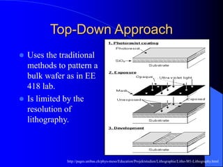
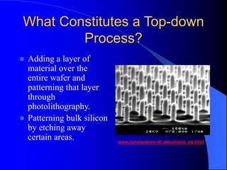
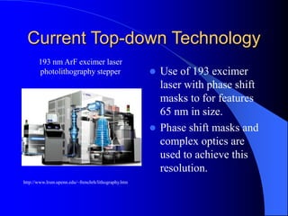
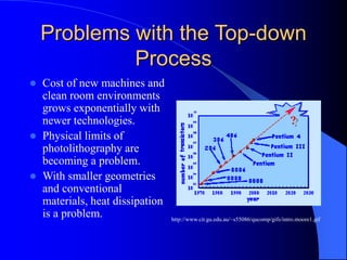
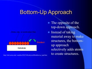
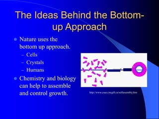
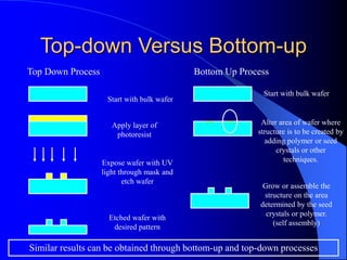
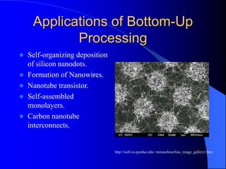
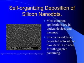
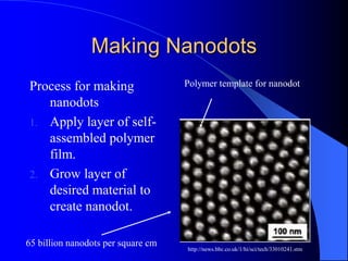
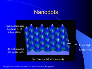
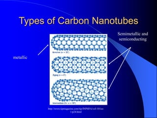
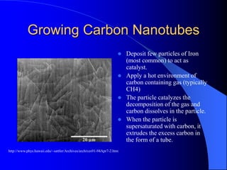
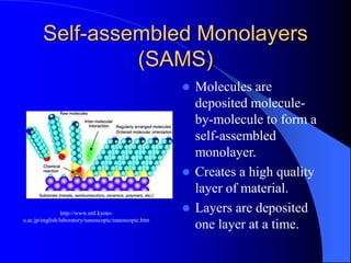
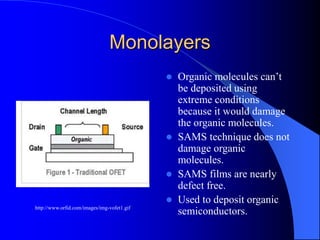
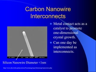
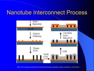
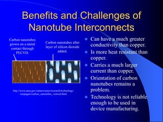
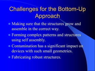
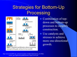
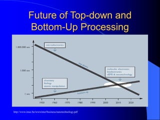


The document discusses top-down and bottom-up processes for manufacturing structures at the nanoscale. Top-down processes start with bulk material and use techniques like lithography and etching to pattern structures, while bottom-up processes build structures from the atomic or molecular scale using self-assembly. Both approaches are needed as bottom-up is required to make smaller structures than lithography allows, and applications include growing carbon nanotubes, nanodots, and using self-assembled monolayers. Challenges of bottom-up include controlling assembly, but the future will see more integration of both top-down and bottom-up nanomanufacturing.


![谷歌留痕技术 [ 𝙩𝙤𝙥 𝟮𝟯𝟯. 𝙘 𝙤𝙢 ]](https://cdn.slidesharecdn.com/ss_thumbnails/top233-260130174328-3833018c-thumbnail.jpg?width=640&height=640&fit=bounds)


