Download as PDF, PPTX


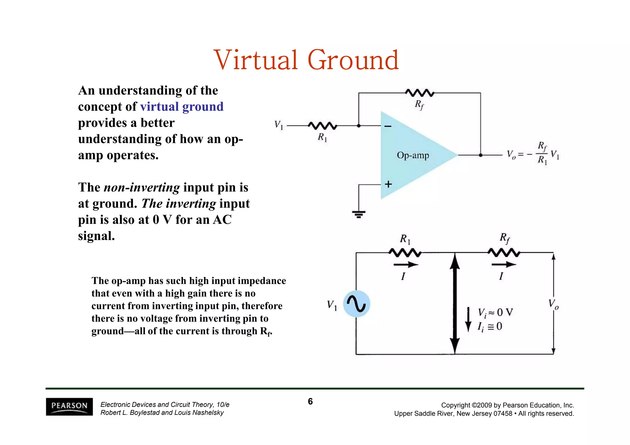

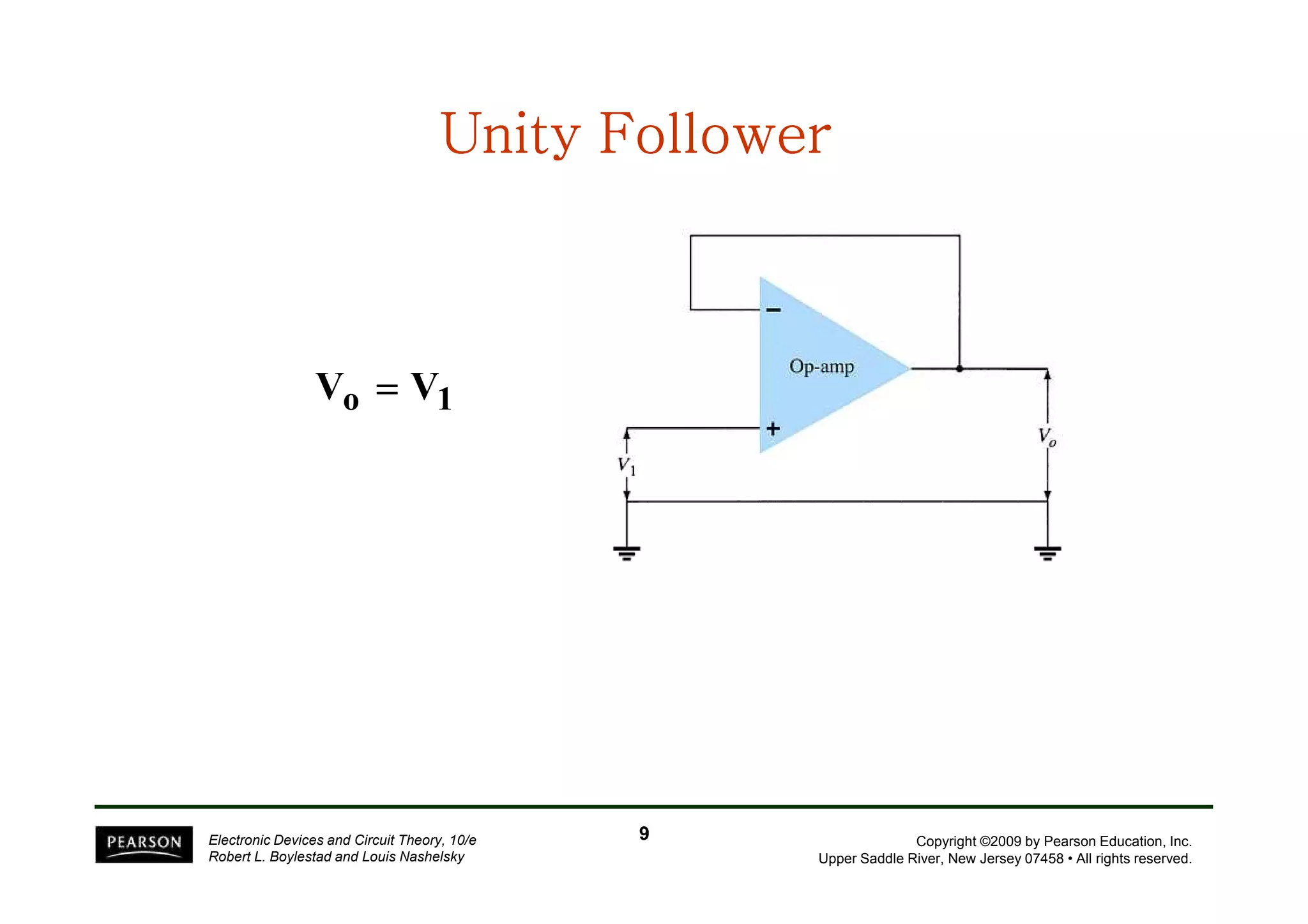


1) An operational amplifier (op-amp) is a high-gain differential amplifier with very high input impedance and low output impedance. It has two input terminals (inverting and non-inverting) and one output terminal. 2) Op-amps can be connected in either open-loop or closed-loop configurations. Open-loop gain can exceed 10,000 but closed-loop with negative feedback reduces gain and improves characteristics. 3) Common op-amp circuits include inverting and non-inverting amplifiers, unity followers, summing amplifiers, integrators, and differentiators.


