Zener Diode and its V-I Characteristics and Applications
This document explains the functioning and characteristics of zener and varactor diodes, including their operation under forward and reverse bias conditions. Zener diodes are primarily used for voltage regulation, where they maintain a constant output voltage despite variations in input voltage or load resistance. Varactor diodes function as variable capacitors, with their capacitance controlled by the reverse bias voltage.
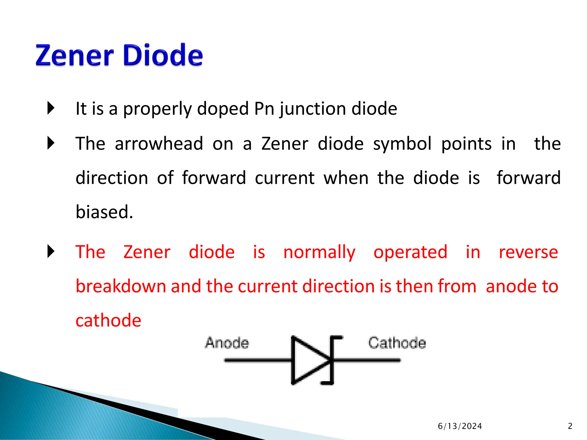
It isa properly doped Pn junction diode
The arrowhead on a Zener diode symbol points in the
direction of forward current when the diode is forward
biased.
The Zener diode is normally operated in reverse
breakdown and the current direction is then from anode to
cathode
6/13/2024 2
3.
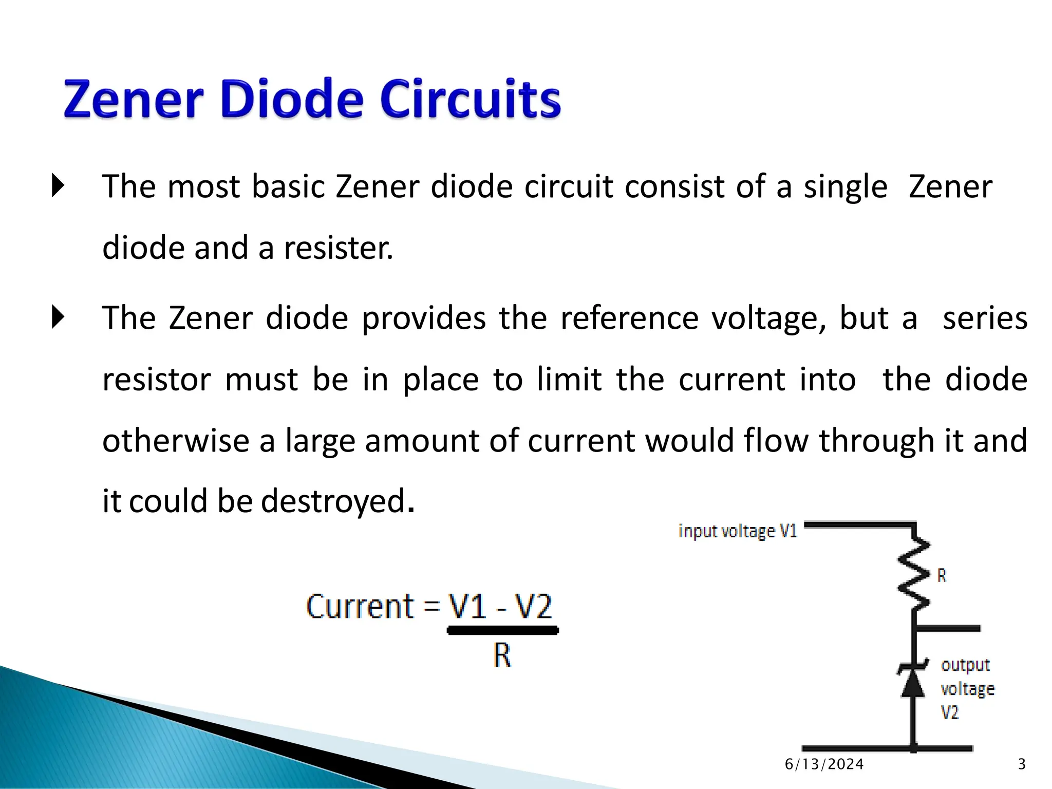
The mostbasic Zener diode circuit consist of a single Zener
diode and a resister.
The Zener diode provides the reference voltage, but a series
resistor must be in place to limit the current into the diode
otherwise a large amount of current would flow through it and
it could be destroyed.
6/13/2024 3
4.
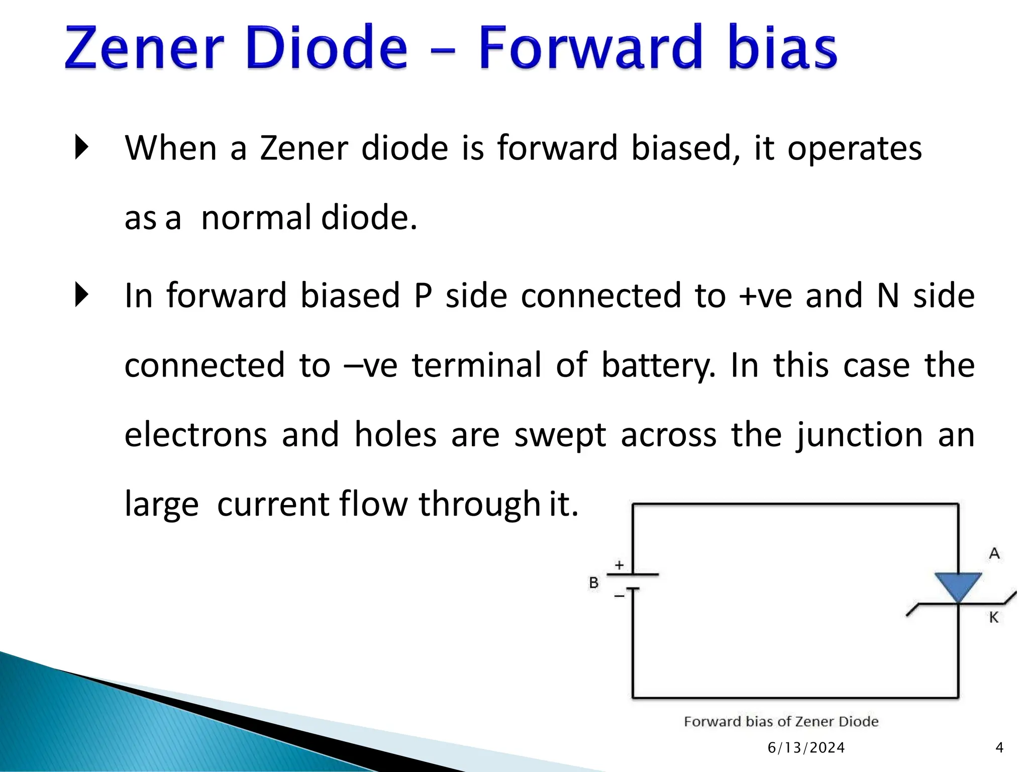
When aZener diode is forward biased, it operates
as a normal diode.
In forward biased P side connected to +ve and N side
connected to –ve terminal of battery. In this case the
electrons and holes are swept across the junction an
large current flow through it.
6/13/2024 4
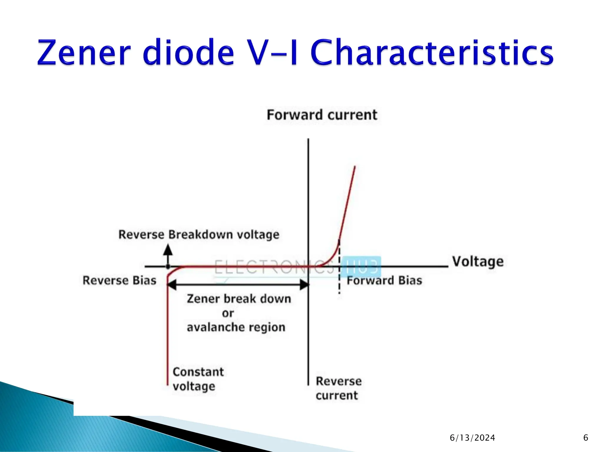
5.
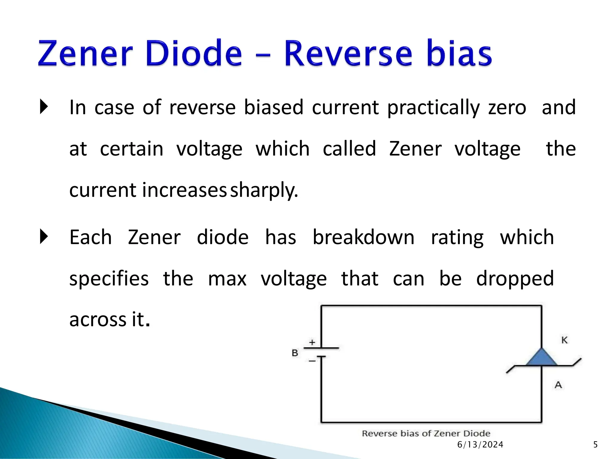
In caseof reverse biased current practically zero and
at certain voltage which called Zener voltage the
current increasessharply.
Each Zener diode has breakdown rating which
specifies the max voltage that can be dropped
across it.
6/13/2024 5
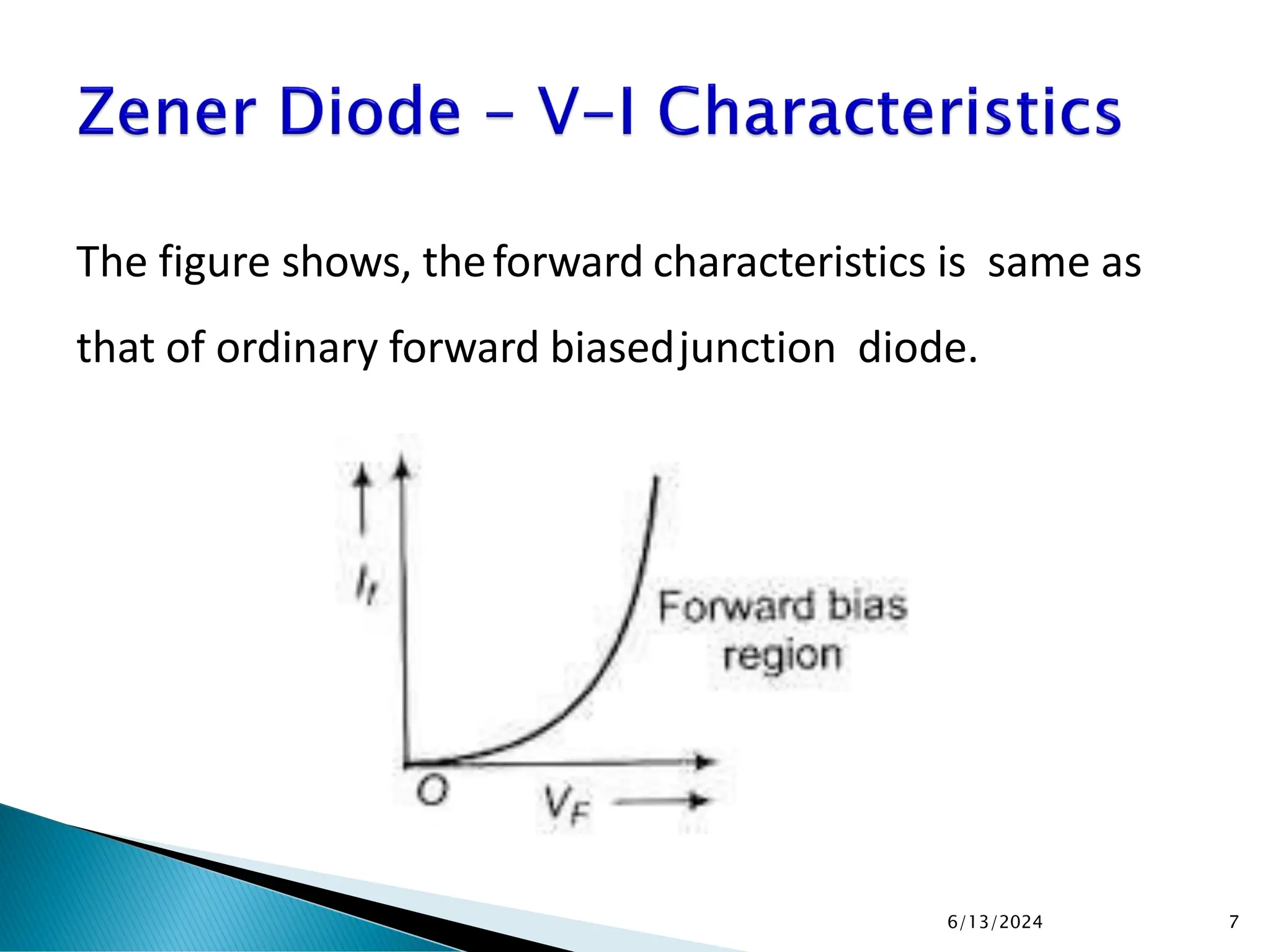
The figure shows,theforward characteristics is same as
that of ordinary forward biasedjunction diode.
6/13/2024 7
8.
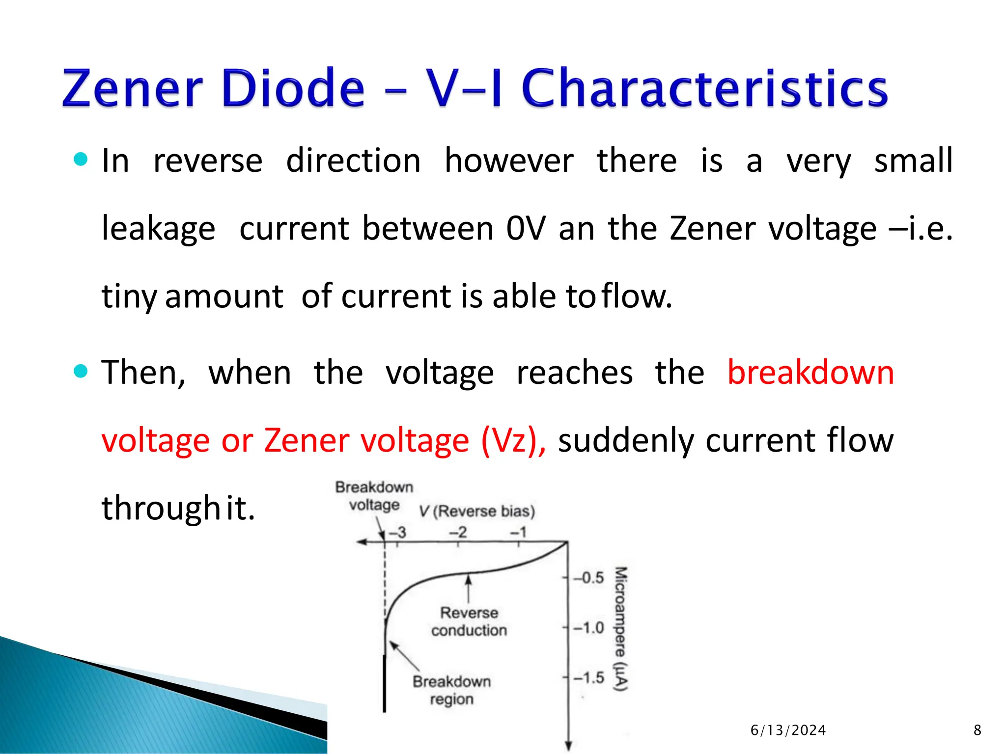
In reversedirection however there is a very small
leakage current between 0V an the Zener voltage –i.e.
tiny amount of current is able toflow.
Then, when the voltage reaches the breakdown
voltage or Zener voltage (Vz), suddenly current flow
throughit.
6/13/2024 8
9.
The Working Principleof zener diode lies in the cause of
breakdown for a diode in reverse biased condition.
Normally there are two types of breakdown.
Zener Breakdown
Avalanche Breakdown
6/13/2024 9
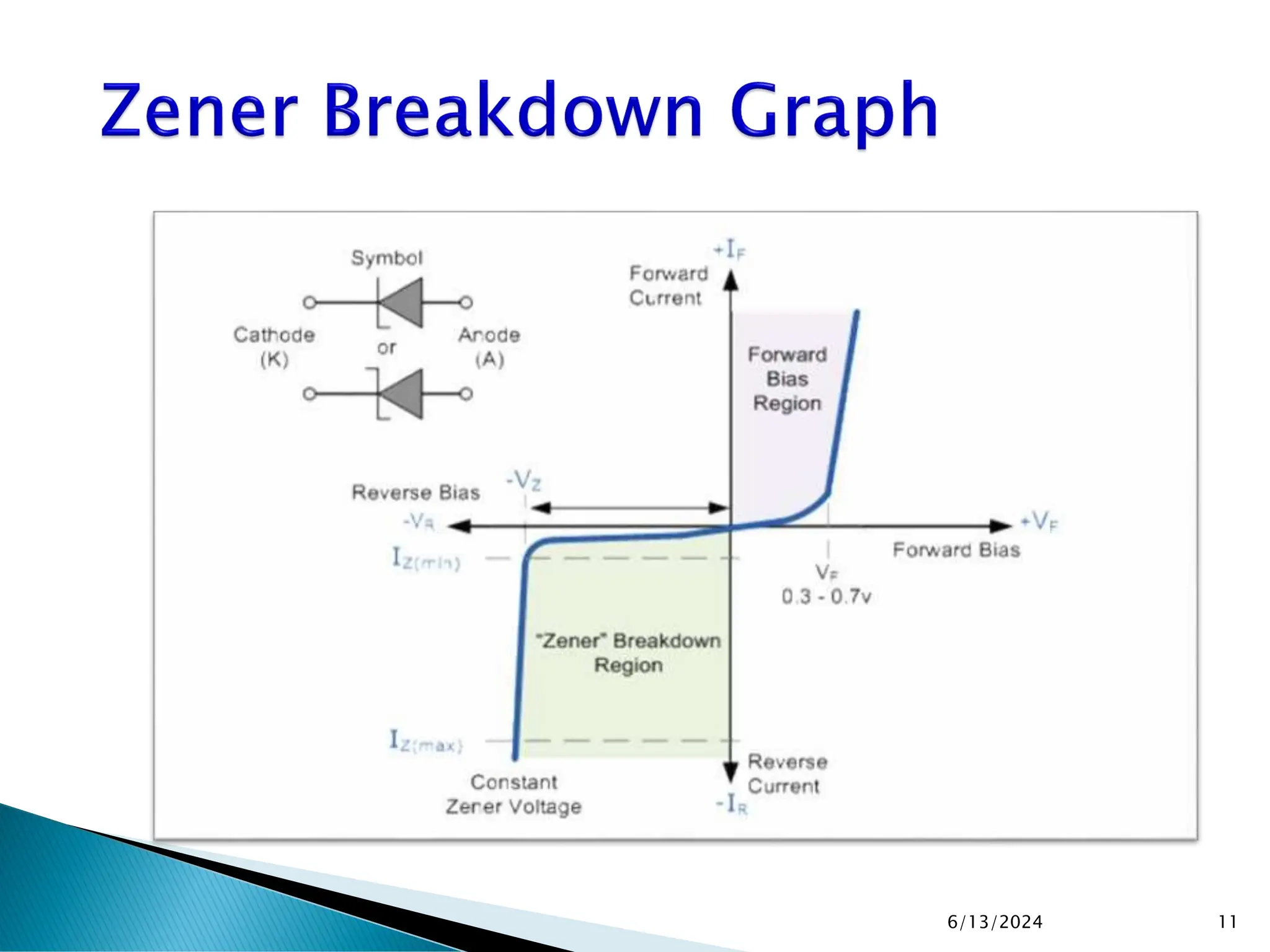
10.
The reversebias on a crystal diode is increased, a critical
voltage, called Breakdown voltage is reached where the
reverse current increases sharply to a high value
The breakdown region is the knee of the reverse
characteristic as shown in graph
The breakdown voltage is sometimes called Zener
Voltage(Vz) and the sudden increase in current is known as
Zener Current
6/13/2024 10
The breakdownor zener voltage depends upon the
amount of doping.
If the diode is heavily doped, depletion layer will be
thin and consequently the breakdown of the junction
will occur at a lower reverse voltage
A lightly doped diode has a higher breakdown voltage
Zener diode is a crystal diode that is properly doped to
have a sharp breakdown voltage
6/13/2024 12
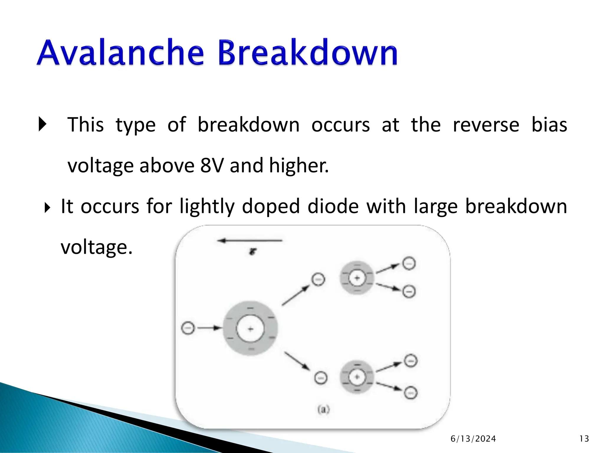
13.
This typeof breakdown occurs at the reverse bias
voltage above 8V and higher.
It occurs for lightly doped diode with large breakdown
voltage.
6/13/2024 13
14.
As minoritycharge carriers (electrons) flow across the
device. They tend to collide with the electrons in the
covalent bond and cause the covalent bond to disrupt. As
voltage increases, the kinetic energy (velocity) of the
electrons also increases. The covalent bonds are more
easily disrupted, causing an increase in electron hole
pairs. The avalanche breakdown voltage increases with
temperature.
6/13/2024 14
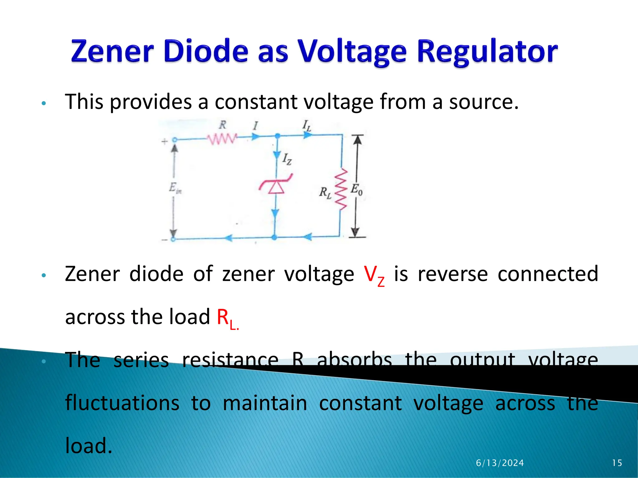
15.
• This providesa constant voltage from a source.
• Zener diode of zener voltage VZ is reverse connected
across the load RL.
• The series resistance R absorbs the output voltage
fluctuations to maintain constant voltage across the
load.
6/13/2024 15
16.
• The zenerwill maintain a constant voltage VZ(=E0)
across the load until input voltage does not fall below
VZ.
• The circuit should be designed in a manner such that
even if the input voltage Ei and load resistance RL
increases over a wide range, the load voltage E0
remains constant.
6/13/2024 16
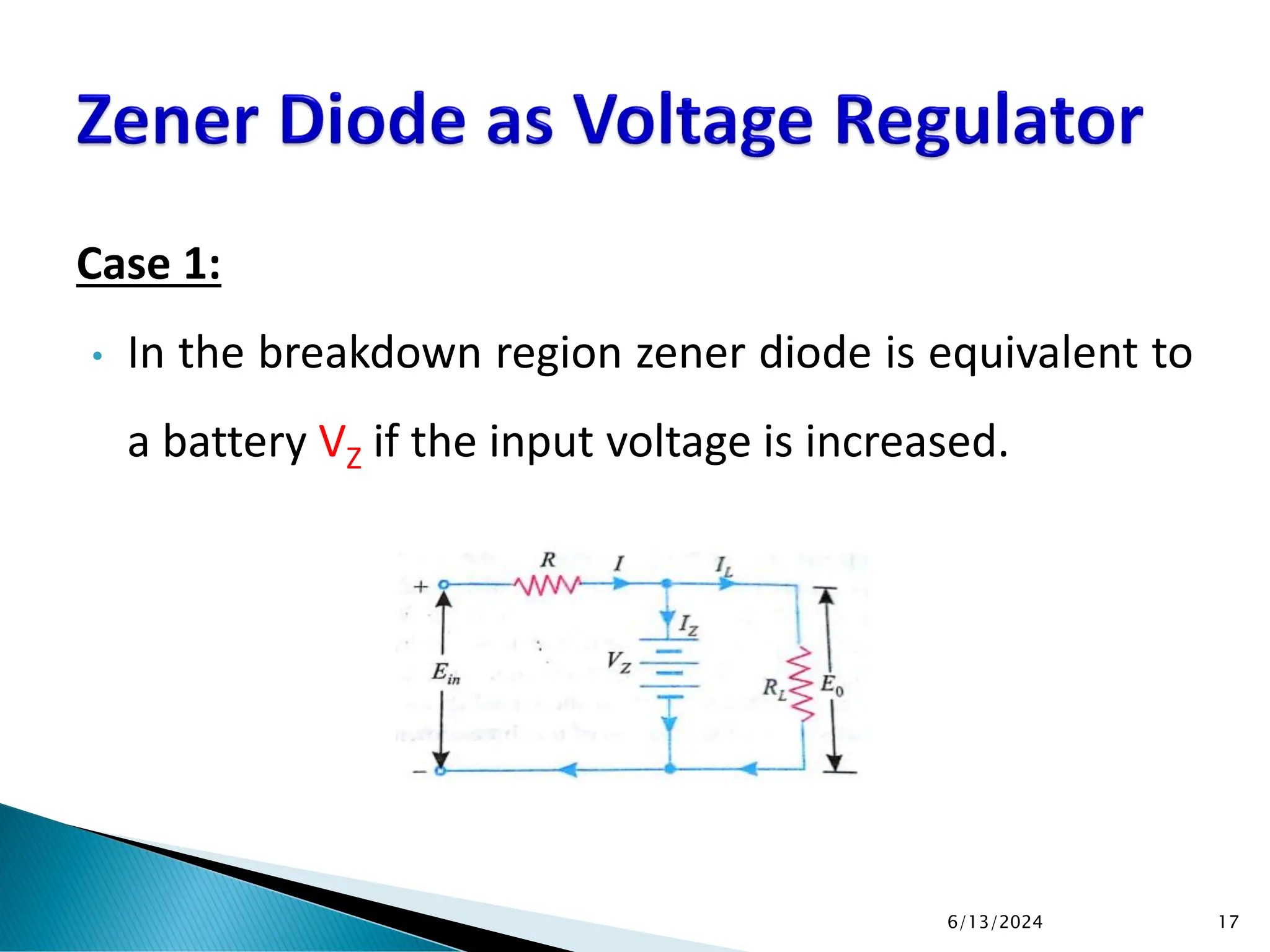
17.
Case 1:
• Inthe breakdown region zener diode is equivalent to
a battery VZ if the input voltage is increased.
6/13/2024 17
18.
Excess voltageis dropped across the series resistance R
which in turn increases the total value of current I.
The zener will conduct the increase of current in I
when the load current remains constant. Hence the
output voltage E0 remains constant.
Case 2:
If the input voltage is constant the load resistance RL
decreases which cause an increase in load current.
6/13/2024 18
19.
Case 2:
• Voltagedrop in a resistor cannot produce an extra
current from a source which will not change as the
zener is within its regulating range.
• Additional load current will come from a decrease in
zener current IZ.
• Voltagedrop across R=Ei-E0
• Current through R=IZ+IL
6/13/2024 19
20.
Varactor Diodeis a reverse biased p-n junction
diode, whose capacitance can be varied
electrically.
It is well known that the operation of the p-n
junction depends on the bias applied which can
be either forward or reverse in characteristic
Under Reverse bias condition, the p-n junction
can be considered to be analogous to a capacitor
where the p and n layers represent the two plates
of the capacitor while the depletion region acts
as a Dielectric separating them.
6/13/2024 20
21.
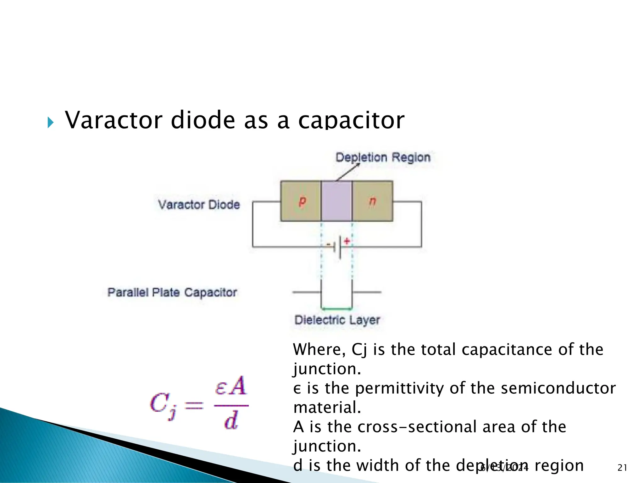
Varactor diodeas a capacitor
6/13/2024 21
Where, Cj is the total capacitance of the
junction.
ε is the permittivity of the semiconductor
material.
A is the cross-sectional area of the
junction.
d is the width of the depletion region
22.
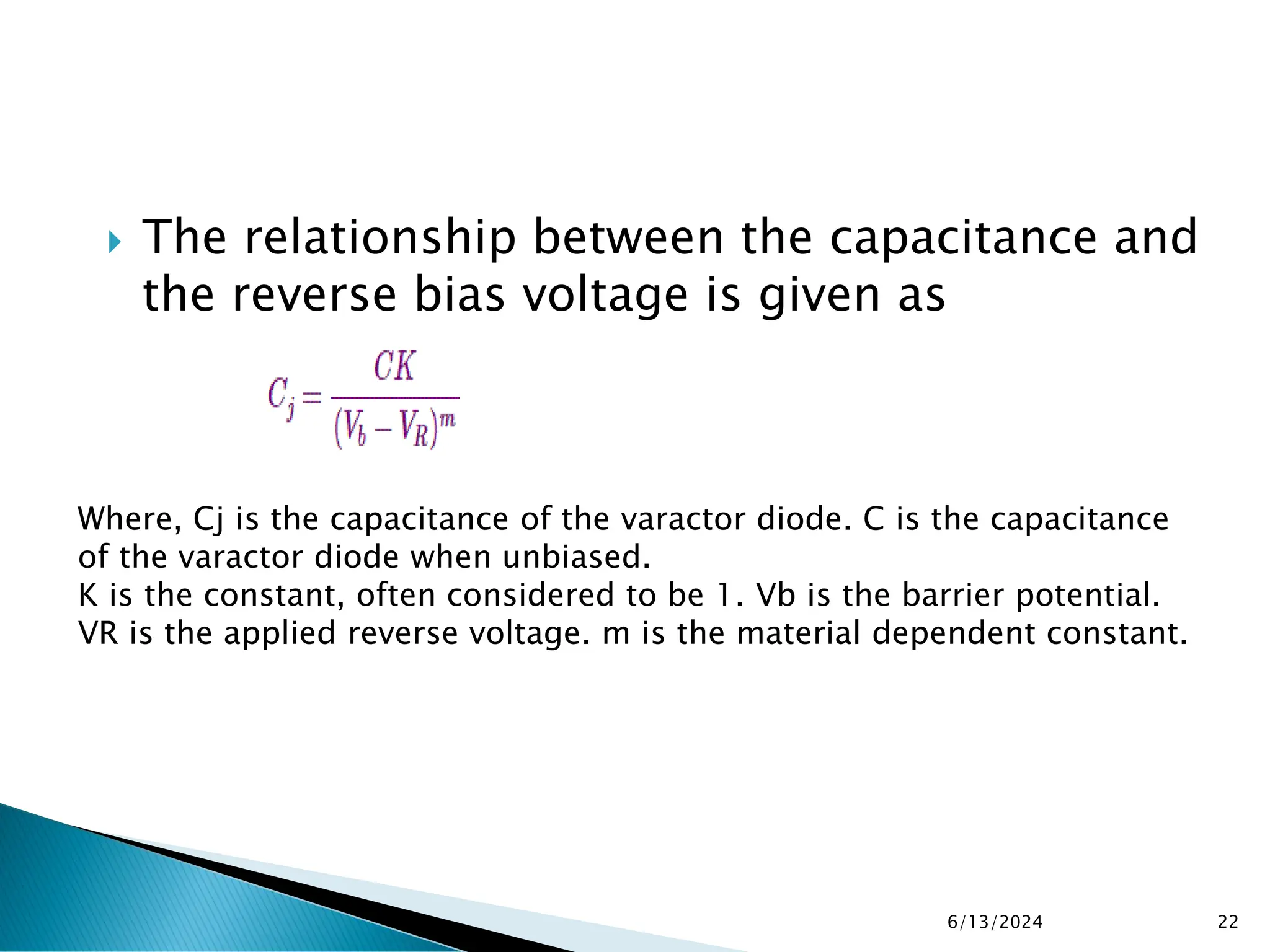
The relationshipbetween the capacitance and
the reverse bias voltage is given as
6/13/2024 22
Where, Cj is the capacitance of the varactor diode. C is the capacitance
of the varactor diode when unbiased.
K is the constant, often considered to be 1. Vb is the barrier potential.
VR is the applied reverse voltage. m is the material dependent constant.
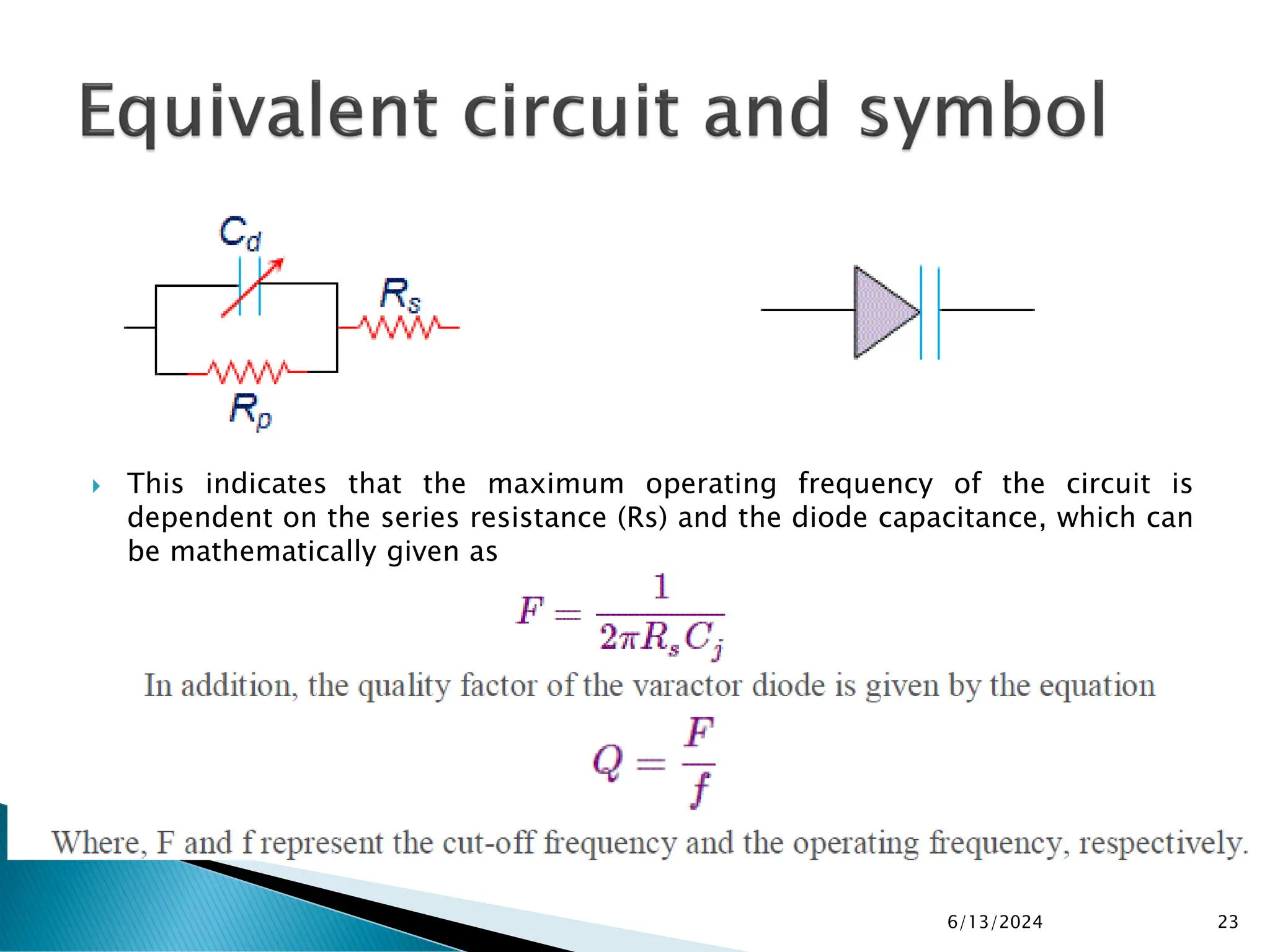
23.
This indicatesthat the maximum operating frequency of the circuit is
dependent on the series resistance (Rs) and the diode capacitance, which can
be mathematically given as
6/13/2024 23
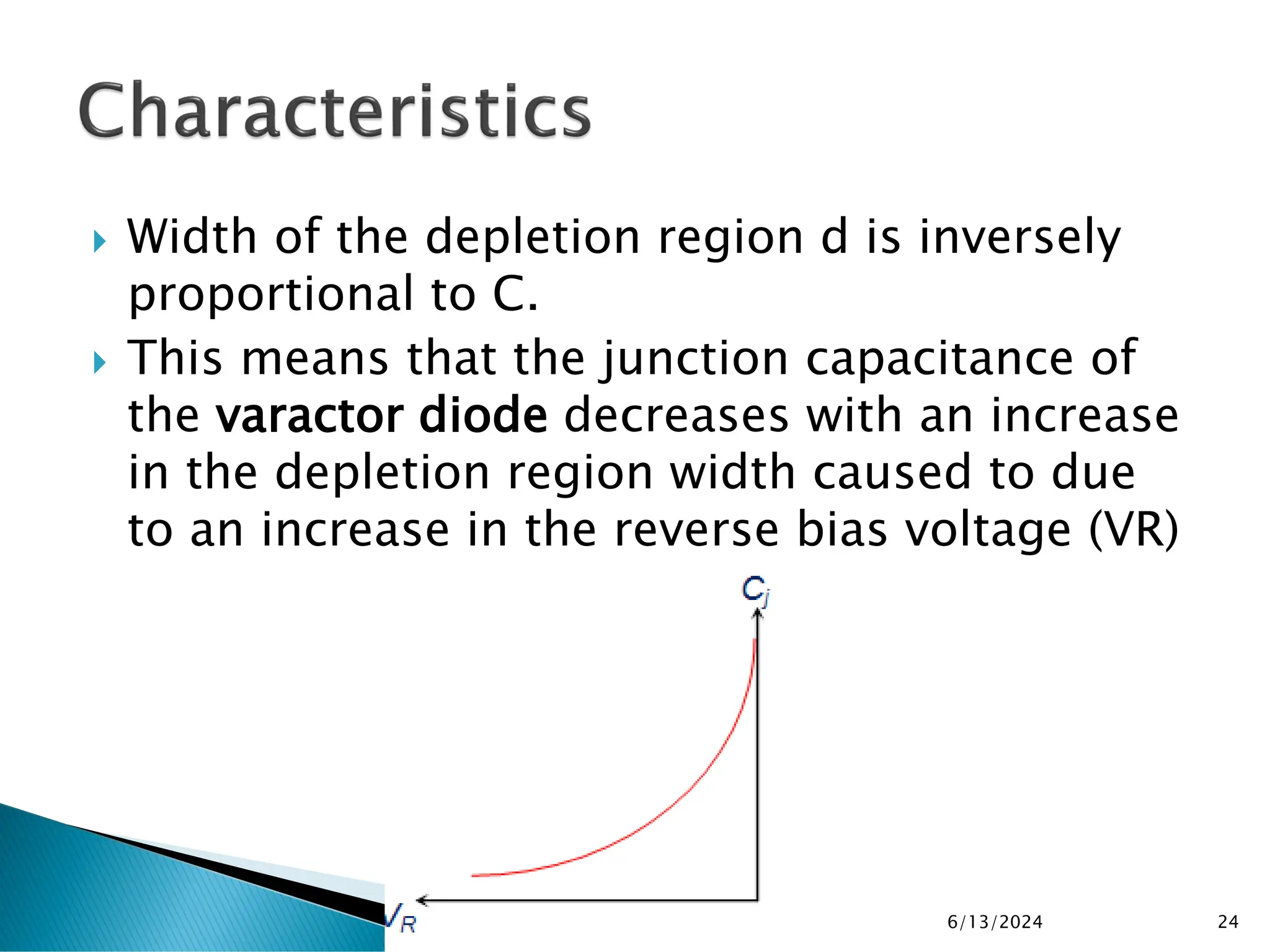
24.
Width ofthe depletion region d is inversely
proportional to C.
This means that the junction capacitance of
the varactor diode decreases with an increase
in the depletion region width caused to due
to an increase in the reverse bias voltage (VR)
6/13/2024 24
25.
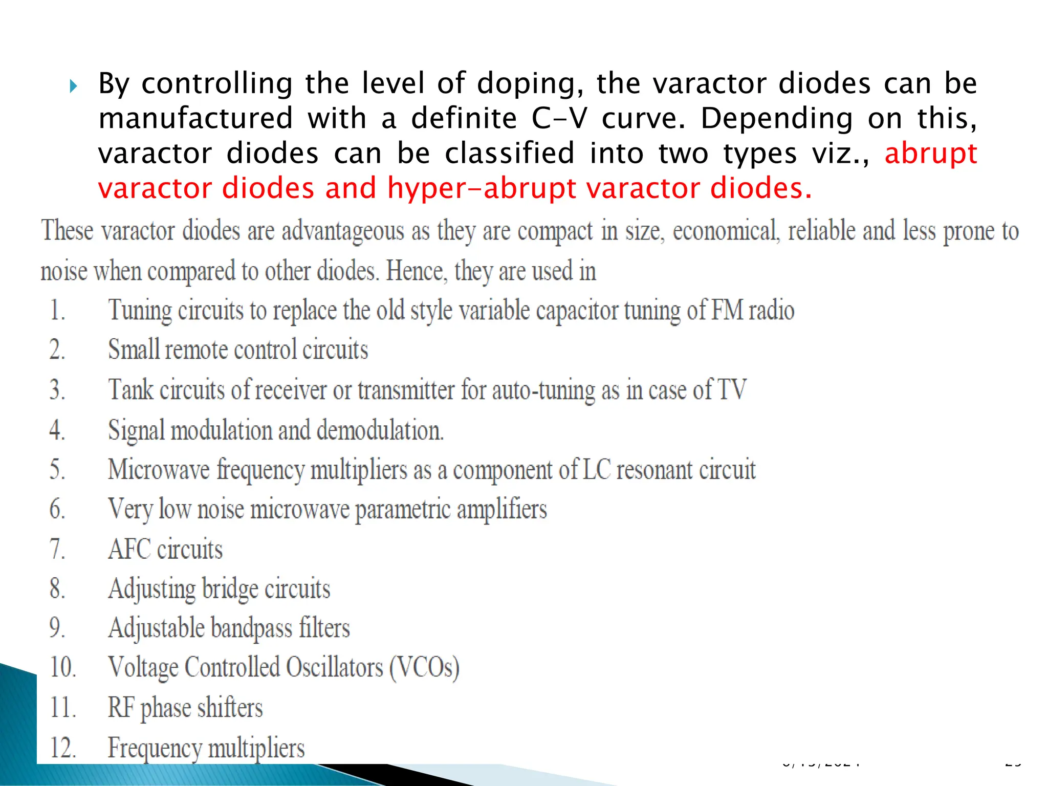
By controllingthe level of doping, the varactor diodes can be
manufactured with a definite C-V curve. Depending on this,
varactor diodes can be classified into two types viz., abrupt
varactor diodes and hyper-abrupt varactor diodes.
6/13/2024 25


![ppt57EC.pptm [Autosaved].pdf............](https://cdn.slidesharecdn.com/ss_thumbnails/ppt57ec-251122120029-3d2c01a0-thumbnail.jpg?width=640&height=640&fit=bounds)