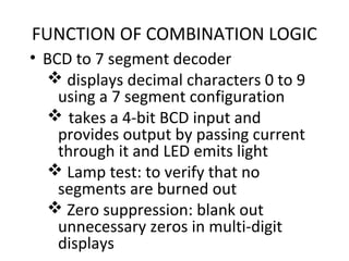
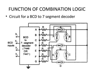
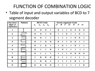
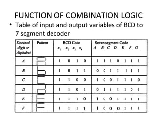
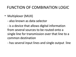
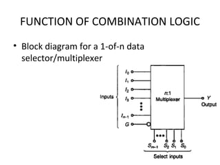
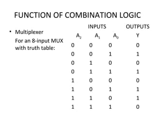
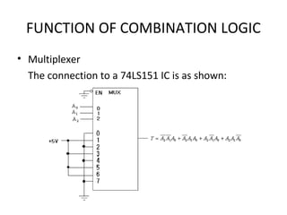
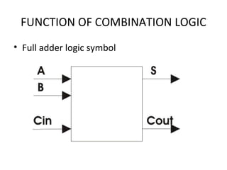
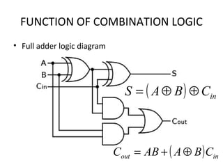
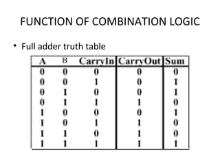
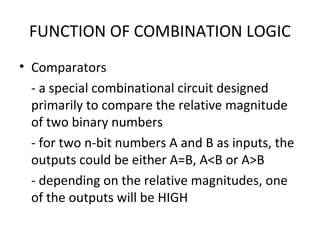
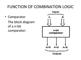
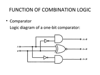
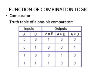
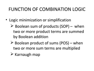
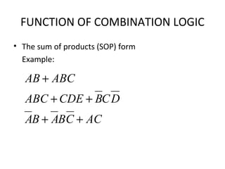
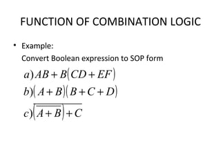
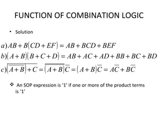
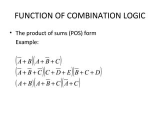
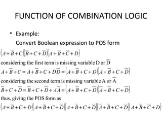
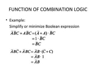
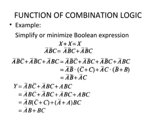
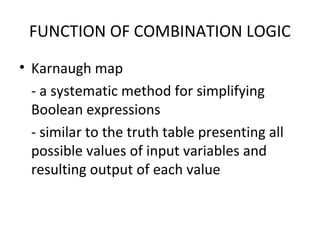
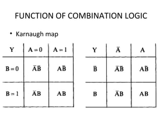
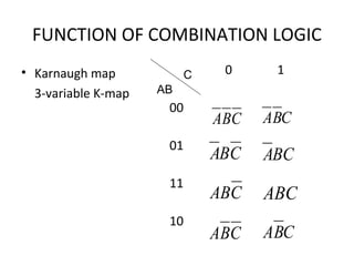
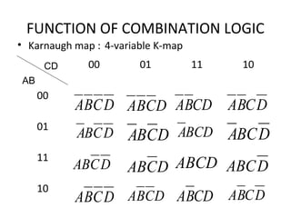
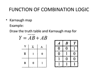
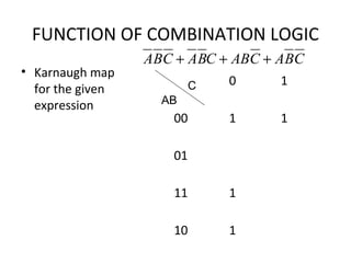
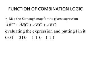
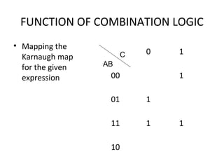
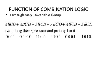
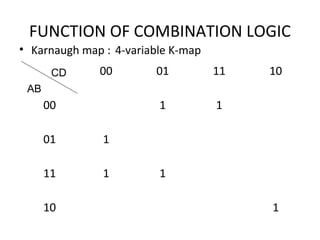
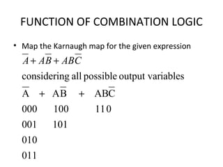
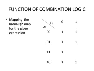
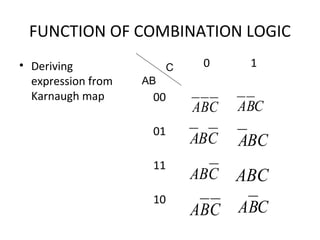
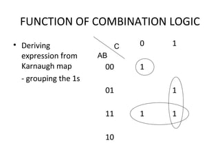
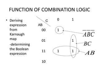
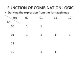
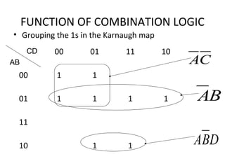
SlideShare a Scribd company logo
DIGITAL ELECTRONICS
CHAPTER 3
DEE 204
DIGITAL ELECTRONICS
• Function of combination logic
Conversion of BCD to 7 segment
decoder.
Multiplexer, tri-state output, fan
out, address, half adder, full
adder, comparator.
Logic minimisation and Karnaugh
maps.
FUNCTION OF COMBINATION LOGIC
• BCD to 7 segment decoder
 displays decimal characters 0 to 9
using a 7 segment configuration
 takes a 4-bit BCD input and
provides output by passing current
through it and LED emits light
 Lamp test: to verify that no
segments are burned out
 Zero suppression: blank out
unnecessary zeros in multi-digit
displays
FUNCTION OF COMBINATION LOGIC
• Circuit for a BCD to 7 segment decoder
FUNCTION OF COMBINATION LOGIC
• Table of input and output variables of BCD to 7
segment decoder
FUNCTION OF COMBINATION LOGIC
• Table of input and output variables of BCD to
7 segment decoder
FUNCTION OF COMBINATION LOGIC
• Multiplexer (MUX)
- also known as data selector
- is a device that allows digital information
from several sources to be routed onto a
single line for transmission over that line to a
common destination
- has several input lines and single output line
FUNCTION OF COMBINATION LOGIC
• Block diagram for a 1-of-n data
selector/multiplexer
FUNCTION OF COMBINATION LOGIC
• Multiplexer
For an 8-input MUX
with truth table:
INPUTS OUTPUTS
A2 A1 A0 Y
0 0 0 0
0 0 1 1
0 1 0 0
0 1 1 1
1 0 0 0
1 0 1 1
1 1 0 1
1 1 1 0
FUNCTION OF COMBINATION LOGIC
• Multiplexer
The connection to a 74LS151 IC is as shown:
FUNCTION OF COMBINATION LOGIC
• Tri-state logic
- normal logic circuits only have two
output states; HIGH and LOW
- in complex digital systems a number of
gate inputs may be required, causing
certain operation problems
FUNCTION OF COMBINATION LOGIC
Related problems:
 Transistor-transistor-logic (TTL)
totem-pole outputs or CMOS active
pull-up/pull-down outputs can’t be
connected together
 open-collector outputs can be
connected together with common
collector but resistor connected
externally, loading and speed
FUNCTION OF COMBINATION LOGIC
• Problems solved by
- developing special circuits with one more
output state known as third state or high
impedance state
- usually used as buffer gates
- modification of NAND gate with addition of
diodes D1 and D2 and an inverter gate
FUNCTION OF COMBINATION LOGIC
• Fan-out
- maximum number of inputs of several gates
that can be driven by the output of a logic
gate
- maximum number of inputs of the same IC
family that the gate can drive maintaining its
output levels within specified limits
FUNCTION OF COMBINATION LOGIC
• Fan-in
- the number of inputs
- at hardware level, it provides
information about the intrinsic speed of
the gate itself
- increases or decreases the propagation
delay
FUNCTION OF COMBINATION LOGIC
• Address:
- location in memory
- indicates the positions of instructions
and data in the memory
- starts with the number ‘0’ and up to the
largest address
FUNCTION OF COMBINATION LOGIC
• Half adder
- adds two bits and produces a sum and carry
output
- accepts two binary digits on inputs and
produces two binary digits on outputs, a sum
bit and a carry bit
Rules of binary addition
0 + 0 = 0
0 + 1 = 1
1 + 0 = 1
1 + 1 = 10
FUNCTION OF COMBINATION LOGIC
• Half-adder
The logic symbol
and logic diagram
for a half-adder:
FUNCTION OF COMBINATION LOGIC
• Half adder
The truth table for a half adder:
FUNCTION OF COMBINATION LOGIC
• Full adder
- has an input carry while the half-adder does
not
- accepts two input bits and an input carry and
generates a sum output and an output carry
FUNCTION OF COMBINATION LOGIC
• Full adder logic symbol
FUNCTION OF COMBINATION LOGIC
• Full adder logic diagram
( ) inout CBAABC ⊕+=
( ) inCBAS ⊕⊕=
FUNCTION OF COMBINATION LOGIC
• Full adder truth table
FUNCTION OF COMBINATION LOGIC
• Comparators
- a special combinational circuit designed
primarily to compare the relative magnitude
of two binary numbers
- for two n-bit numbers A and B as inputs, the
outputs could be either A=B, A<B or A>B
- depending on the relative magnitudes, one
of the outputs will be HIGH
FUNCTION OF COMBINATION LOGIC
• Comparator
The block diagram
of a n-bit
comparator:
FUNCTION OF COMBINATION LOGIC
• Comparator
Logic diagram of a one-bit comparator:
FUNCTION OF COMBINATION LOGIC
• Comparator
Truth table of a one-bit comparator:
FUNCTION OF COMBINATION LOGIC
• Logic minimization or simplification
 Boolean sum of products (SOP) – when
two or more product terms are summed
by Boolean addition
 Boolean product of sums (POS) – when
two or more sum terms are multiplied
 Karnaugh map
FUNCTION OF COMBINATION LOGIC
• The sum of products (SOP) form
Example:
ACCBABA
DCBCDEABC
ABCAB
++
++
+
FUNCTION OF COMBINATION LOGIC
• Example:
Convert Boolean expression to SOP form
( )
( )( )
( ) CBAc
DCBBAb
EFCDBABa
++
+++
++
)
)
)
FUNCTION OF COMBINATION LOGIC
• Solution
 An SOP expression is ‘1’ if one or more of the product terms
is ‘1’
( )
( )( )
( ) ( ) ( ) CBCACBACBACBAc
BDBCBBADACABDCBBAb
BEFBCDABEFCDBABa
+=+=+=++
+++++=+++
++=++
)
)
)
FUNCTION OF COMBINATION LOGIC
• The product of sums (POS) form
Example:
( )( )
( )( )( )
( )( )( )CACBABA
DCBEDCCBA
CBABA
++++
++++++
+++
FUNCTION OF COMBINATION LOGIC
• Example:
Convert Boolean expression to POS form
( )( )( )
( )( )
( )( )
( )( )( )( )( )DCBADCBADCBADCBADCBA
DCBADCBAAADCBDCB
DCBADCBADDCBACBA
DCBADCBCBA
+++++++++++++++
++++++=+++=++
++++++=+++=++
+++++++
asformPOSthegivingthus,
AorAvariablemissingistermsecondthegconsiderin
DorDvariablemissingisfirst termthegconsiderin
FUNCTION OF COMBINATION LOGIC
• Example:
Simplify or minimize Boolean expression
FUNCTION OF COMBINATION LOGIC
• Example:
Simplify or minimize Boolean expression
FUNCTION OF COMBINATION LOGIC
• Karnaugh map
- a systematic method for simplifying
Boolean expressions
- similar to the truth table presenting all
possible values of input variables and
resulting output of each value
FUNCTION OF COMBINATION LOGIC
• Karnaugh map
FUNCTION OF COMBINATION LOGIC
• Karnaugh map
3-variable K-map
0 1
00
01
11
10
C
AB
CBA CBA
CBA BCA
CAB ABC
CBA CBA
FUNCTION OF COMBINATION LOGIC
• Karnaugh map : 4-variable K-map
00 01 11 10
00
01
11
10
CD
AB
DCBA DCBA
DCBA DCBA
DCAB DCAB
DCBA DCBA
CDBA DCBA
BCDA DBCA
ABCD DABC
CDBA DCBA
FUNCTION OF COMBINATION LOGIC
• Karnaugh map
Example:
Draw the truth table and Karnaugh map for
ABBAY +=
FUNCTION OF COMBINATION LOGIC
• Karnaugh map
for the given
expression
0 1
00 1 1
01
11 1
10 1
C
AB
CBACABCBACBA +++
FUNCTION OF COMBINATION LOGIC
• Map the Karnaugh map for the given expression
111011010100
itin1puttingandexpressiontheevaluating
ABCCABCBACBA +++
FUNCTION OF COMBINATION LOGIC
• Mapping the
Karnaugh map
for the given
expression
0 1
00 1
01 1
11 1 1
10
C
AB
FUNCTION OF COMBINATION LOGIC
• Karnaugh map : 4-variable K-map
010110000011101100101100
itin1puttingandexpressiontheevaluating
DCBADCBADCABDCABDCBACDBA +++++
FUNCTION OF COMBINATION LOGIC
• Karnaugh map : 4-variable K-map
00 01 11 10
00 1 1
01 1
11 1 1
10 1
CD
AB
FUNCTION OF COMBINATION LOGIC
• Map the Karnaugh map for the given expression
011
010
101001
011100000
CABBAA
iablesoutput varpossibleallgconsiderin
++
++ CABBAA
FUNCTION OF COMBINATION LOGIC
• Mapping the
Karnaugh map
for the given
expression
0 1
00 1 1
01 1 1
11 1
10 1 1
C
AB
FUNCTION OF COMBINATION LOGIC
• Deriving
expression from
Karnaugh map
0 1
00
01
11
10
C
AB
CBA CBA
CBA BCA
CAB ABC
CBA CBA
FUNCTION OF COMBINATION LOGIC
• Deriving
expression from
Karnaugh map
- grouping the 1s
0 1
00 1
01 1
11 1 1
10
C
AB
FUNCTION OF COMBINATION LOGIC
• Deriving
expression
from
Karnaugh
map
-determining
the Boolean
expression
0 1
00 1
01 1
11 1 1
10
C
AB
CBA
BC
AB
FUNCTION OF COMBINATION LOGIC
• Deriving the expression from the Karnaugh map
00 01 11 10
00 1 1
01 1 1 1 1
11
10 1 1
CD
AB
FUNCTION OF COMBINATION LOGIC
• Grouping the 1s in the Karnaugh map
00 01 11 10
00 1 1
01 1 1 1 1
11
10 1 1
CD
AB CA
BA
DBA

More Related Content

What's hot

Encoder and decoder
Encoder and decoderEncoder and decoder
Encoder and decoder
Then Murugeshwari
 
Combinational logic circuits by Tahir Yasin
Combinational logic circuits by Tahir YasinCombinational logic circuits by Tahir Yasin
Combinational logic circuits by Tahir Yasin
TAHIR YASIN
 
Combinational circuit
Combinational circuitCombinational circuit
Combinational circuit
Satya P. Joshi
 
Digital Logic circuit
Digital Logic circuitDigital Logic circuit
Digital Logic circuit
kavitha muneeshwaran
 
Digital Logic Design
Digital Logic Design Digital Logic Design
Digital Logic Design
Vaagdevi College of Engineering
 
Introduction to digital logic
Introduction to digital logicIntroduction to digital logic
Introduction to digital logic
Kamal Acharya
 
Combinational logic
Combinational logicCombinational logic
Combinational logic
Ezeokafor Chibueze
 
Dld ppt
Dld  pptDld  ppt
Combinational circuit
Combinational circuitCombinational circuit
Combinational circuit
sabina deshar
 
STLD-Combinational logic design
STLD-Combinational  logic design STLD-Combinational  logic design
STLD-Combinational logic design
Abhinay Potlabathini
 
DEL LAB MANUAL
DEL LAB MANUALDEL LAB MANUAL
Introduction of Combinational logic circuits & half adder
Introduction of Combinational logic circuits & half adderIntroduction of Combinational logic circuits & half adder
Introduction of Combinational logic circuits & half adder
hymalakshmitirumani
 
decade counter
decade counterdecade counter
decade counter
Abhishek Sainkar
 
BCD Counter
BCD CounterBCD Counter
BCD Counter
Ahmed A. Arefin
 
Combinational logic With Multiplexers and Decoders
Combinational logic With Multiplexers and DecodersCombinational logic With Multiplexers and Decoders
Combinational logic With Multiplexers and Decoders
Harsh Parmar
 
Encoder decoder Adc LDR &7 Segment PPT
Encoder decoder Adc LDR &7 Segment  PPTEncoder decoder Adc LDR &7 Segment  PPT
Encoder decoder Adc LDR &7 Segment PPT
Engineering Garage V=ir
 
Combinational circuits
Combinational circuitsCombinational circuits
Combinational circuits
Jamnas Mundakkutty A
 
Digital Electronics (EC8392) UNIT-II -PPT-S.SESHA VIDHYA/ ASP/ECE
Digital Electronics (EC8392) UNIT-II -PPT-S.SESHA VIDHYA/ ASP/ECEDigital Electronics (EC8392) UNIT-II -PPT-S.SESHA VIDHYA/ ASP/ECE
Digital Electronics (EC8392) UNIT-II -PPT-S.SESHA VIDHYA/ ASP/ECE
SeshaVidhyaS
 
Bcd to 7 segment display
Bcd to 7 segment displayBcd to 7 segment display
Bcd to 7 segment display
Maulik Sanchela
 

What's hot (20)

Encoder and decoder
Encoder and decoderEncoder and decoder
Encoder and decoder
 
Combinational logic circuits by Tahir Yasin
Combinational logic circuits by Tahir YasinCombinational logic circuits by Tahir Yasin
Combinational logic circuits by Tahir Yasin
 
Combinational circuit
Combinational circuitCombinational circuit
Combinational circuit
 
Digital Logic circuit
Digital Logic circuitDigital Logic circuit
Digital Logic circuit
 
Digital Logic Design
Digital Logic Design Digital Logic Design
Digital Logic Design
 
Introduction to digital logic
Introduction to digital logicIntroduction to digital logic
Introduction to digital logic
 
Combinational logic
Combinational logicCombinational logic
Combinational logic
 
Dld ppt
Dld  pptDld  ppt
Dld ppt
 
Combinational circuit
Combinational circuitCombinational circuit
Combinational circuit
 
STLD-Combinational logic design
STLD-Combinational  logic design STLD-Combinational  logic design
STLD-Combinational logic design
 
DEL LAB MANUAL
DEL LAB MANUALDEL LAB MANUAL
DEL LAB MANUAL
 
Introduction of Combinational logic circuits & half adder
Introduction of Combinational logic circuits & half adderIntroduction of Combinational logic circuits & half adder
Introduction of Combinational logic circuits & half adder
 
decade counter
decade counterdecade counter
decade counter
 
BCD Counter
BCD CounterBCD Counter
BCD Counter
 
Combinational logic With Multiplexers and Decoders
Combinational logic With Multiplexers and DecodersCombinational logic With Multiplexers and Decoders
Combinational logic With Multiplexers and Decoders
 
Encoder decoder Adc LDR &7 Segment PPT
Encoder decoder Adc LDR &7 Segment  PPTEncoder decoder Adc LDR &7 Segment  PPT
Encoder decoder Adc LDR &7 Segment PPT
 
Combinational circuits
Combinational circuitsCombinational circuits
Combinational circuits
 
Digital Electronics (EC8392) UNIT-II -PPT-S.SESHA VIDHYA/ ASP/ECE
Digital Electronics (EC8392) UNIT-II -PPT-S.SESHA VIDHYA/ ASP/ECEDigital Electronics (EC8392) UNIT-II -PPT-S.SESHA VIDHYA/ ASP/ECE
Digital Electronics (EC8392) UNIT-II -PPT-S.SESHA VIDHYA/ ASP/ECE
 
De lab manual
De lab manualDe lab manual
De lab manual
 
Bcd to 7 segment display
Bcd to 7 segment displayBcd to 7 segment display
Bcd to 7 segment display
 

Viewers also liked

Multiplexing
MultiplexingMultiplexing
Multiplexing
Mohammad Bappy
 
311 communication system concepts
311 communication system concepts311 communication system concepts
311 communication system concepts
Mohammad Bappy
 
Broadcasting and video systems
Broadcasting and video systemsBroadcasting and video systems
Broadcasting and video systems
Mohammad Bappy
 
Error control coding
Error control codingError control coding
Error control coding
Mohammad Bappy
 
311 linear modulation
311 linear modulation311 linear modulation
311 linear modulation
Mohammad Bappy
 
Digital communication methods
Digital communication methodsDigital communication methods
Digital communication methods
Mohammad Bappy
 
Digital e chap 4
Digital e   chap 4Digital e   chap 4
Digital e chap 4
Mohammad Bappy
 
Day2 session3 multi-criteria-analysis
Day2 session3 multi-criteria-analysisDay2 session3 multi-criteria-analysis
Day2 session3 multi-criteria-analysis
OECD Environment
 
311 angle modulation
311 angle modulation311 angle modulation
311 angle modulation
Mohammad Bappy
 
Antenna and propagation
Antenna and propagationAntenna and propagation
Antenna and propagation
Mohammad Bappy
 
311 pulse modulation
311 pulse modulation311 pulse modulation
311 pulse modulation
Mohammad Bappy
 
311 introduction to communication system
311 introduction to communication system311 introduction to communication system
311 introduction to communication system
Mohammad Bappy
 
Eeng 3810 chapter 4
Eeng 3810 chapter 4Eeng 3810 chapter 4
Eeng 3810 chapter 4
Mohammad Bappy
 
Digital design chap 5
Digital design   chap 5Digital design   chap 5
Digital design chap 5
Mohammad Bappy
 
Policy analysis
Policy analysisPolicy analysis
Policy analysisuma107
 
Cost benefit analysis
Cost benefit analysisCost benefit analysis
Cost-benefit analysis
Cost-benefit analysisCost-benefit analysis
Cost-benefit analysis
Soniya Balan
 

Viewers also liked (18)

Final version resub
Final version resubFinal version resub
Final version resub
 
Multiplexing
MultiplexingMultiplexing
Multiplexing
 
311 communication system concepts
311 communication system concepts311 communication system concepts
311 communication system concepts
 
Broadcasting and video systems
Broadcasting and video systemsBroadcasting and video systems
Broadcasting and video systems
 
Error control coding
Error control codingError control coding
Error control coding
 
311 linear modulation
311 linear modulation311 linear modulation
311 linear modulation
 
Digital communication methods
Digital communication methodsDigital communication methods
Digital communication methods
 
Digital e chap 4
Digital e   chap 4Digital e   chap 4
Digital e chap 4
 
Day2 session3 multi-criteria-analysis
Day2 session3 multi-criteria-analysisDay2 session3 multi-criteria-analysis
Day2 session3 multi-criteria-analysis
 
311 angle modulation
311 angle modulation311 angle modulation
311 angle modulation
 
Antenna and propagation
Antenna and propagationAntenna and propagation
Antenna and propagation
 
311 pulse modulation
311 pulse modulation311 pulse modulation
311 pulse modulation
 
311 introduction to communication system
311 introduction to communication system311 introduction to communication system
311 introduction to communication system
 
Eeng 3810 chapter 4
Eeng 3810 chapter 4Eeng 3810 chapter 4
Eeng 3810 chapter 4
 
Digital design chap 5
Digital design   chap 5Digital design   chap 5
Digital design chap 5
 
Policy analysis
Policy analysisPolicy analysis
Policy analysis
 
Cost benefit analysis
Cost benefit analysisCost benefit analysis
Cost benefit analysis
 
Cost-benefit analysis
Cost-benefit analysisCost-benefit analysis
Cost-benefit analysis
 

Similar to Digital design chap 3

Lec 05 - Combinational Logic
Lec 05 - Combinational LogicLec 05 - Combinational Logic
Lec 05 - Combinational Logic
Vajira Thambawita
 
Combinational circuit
Combinational circuitCombinational circuit
Combinational circuit
SIVALAKSHMIPANNEERSE
 
combinational-circuit (1).ppt
combinational-circuit (1).pptcombinational-circuit (1).ppt
combinational-circuit (1).ppt
ThanmayiKumar
 
Digital Electronics-Unit II.pdf
Digital Electronics-Unit II.pdfDigital Electronics-Unit II.pdf
Digital Electronics-Unit II.pdf
Kannan Kanagaraj
 
Digital electronics lab
Digital electronics labDigital electronics lab
Digital electronics lab
swatymanoja
 
Satish Chandra_020686.pptx
Satish Chandra_020686.pptxSatish Chandra_020686.pptx
Satish Chandra_020686.pptx
Satish Chandra
 
DLD Lecture No 18 Analysis and Design of Combinational Circuit.pptx
DLD Lecture No 18 Analysis and Design of Combinational Circuit.pptxDLD Lecture No 18 Analysis and Design of Combinational Circuit.pptx
DLD Lecture No 18 Analysis and Design of Combinational Circuit.pptx
SaveraAyub2
 
Digital design chap 2
Digital design    chap 2Digital design    chap 2
Digital design chap 2
Mohammad Bappy
 
Combinational and sequential logic
Combinational and sequential logicCombinational and sequential logic
Combinational and sequential logic
Deepak John
 
Cost-Based Optimizer in Apache Spark 2.2
Cost-Based Optimizer in Apache Spark 2.2 Cost-Based Optimizer in Apache Spark 2.2
Cost-Based Optimizer in Apache Spark 2.2
Databricks
 
Cost-Based Optimizer in Apache Spark 2.2 Ron Hu, Sameer Agarwal, Wenchen Fan ...
Cost-Based Optimizer in Apache Spark 2.2 Ron Hu, Sameer Agarwal, Wenchen Fan ...Cost-Based Optimizer in Apache Spark 2.2 Ron Hu, Sameer Agarwal, Wenchen Fan ...
Cost-Based Optimizer in Apache Spark 2.2 Ron Hu, Sameer Agarwal, Wenchen Fan ...
Databricks
 
Combinational Ckt.pdf
Combinational Ckt.pdfCombinational Ckt.pdf
Combinational Ckt.pdf
ShivarkarSandip
 
32-bit unsigned multiplier by using CSLA & CLAA
32-bit unsigned multiplier by using CSLA &  CLAA32-bit unsigned multiplier by using CSLA &  CLAA
32-bit unsigned multiplier by using CSLA & CLAA
Ganesh Sambasivarao
 
Ieee project reversible logic gates by_amit
Ieee project reversible logic gates  by_amitIeee project reversible logic gates  by_amit
Ieee project reversible logic gates by_amit
Amith Bhonsle
 
Ieee project reversible logic gates by_amit
Ieee project reversible logic gates  by_amitIeee project reversible logic gates  by_amit
Ieee project reversible logic gates by_amit
Amith Bhonsle
 
implementation and comparision of effective area efficient architecture for CSLA
implementation and comparision of effective area efficient architecture for CSLAimplementation and comparision of effective area efficient architecture for CSLA
implementation and comparision of effective area efficient architecture for CSLA
venkatesh nayakoti
 
Chapter 5_combinational logic (EEEg4302).pdf
Chapter 5_combinational logic (EEEg4302).pdfChapter 5_combinational logic (EEEg4302).pdf
Chapter 5_combinational logic (EEEg4302).pdf
TamiratDejene1
 
Design of chip controller
Design of chip controllerDesign of chip controller
Design of chip controller
asha
 
Combinational circuits
Combinational circuitsCombinational circuits
Combinational circuits
Nabarun Chakraborty
 
EMBEDDED SYSTEM BASICS
EMBEDDED SYSTEM BASICSEMBEDDED SYSTEM BASICS
EMBEDDED SYSTEM BASICS
RANAALIMAJEEDRAJPUT
 

Similar to Digital design chap 3 (20)

Lec 05 - Combinational Logic
Lec 05 - Combinational LogicLec 05 - Combinational Logic
Lec 05 - Combinational Logic
 
Combinational circuit
Combinational circuitCombinational circuit
Combinational circuit
 
combinational-circuit (1).ppt
combinational-circuit (1).pptcombinational-circuit (1).ppt
combinational-circuit (1).ppt
 
Digital Electronics-Unit II.pdf
Digital Electronics-Unit II.pdfDigital Electronics-Unit II.pdf
Digital Electronics-Unit II.pdf
 
Digital electronics lab
Digital electronics labDigital electronics lab
Digital electronics lab
 
Satish Chandra_020686.pptx
Satish Chandra_020686.pptxSatish Chandra_020686.pptx
Satish Chandra_020686.pptx
 
DLD Lecture No 18 Analysis and Design of Combinational Circuit.pptx
DLD Lecture No 18 Analysis and Design of Combinational Circuit.pptxDLD Lecture No 18 Analysis and Design of Combinational Circuit.pptx
DLD Lecture No 18 Analysis and Design of Combinational Circuit.pptx
 
Digital design chap 2
Digital design    chap 2Digital design    chap 2
Digital design chap 2
 
Combinational and sequential logic
Combinational and sequential logicCombinational and sequential logic
Combinational and sequential logic
 
Cost-Based Optimizer in Apache Spark 2.2
Cost-Based Optimizer in Apache Spark 2.2 Cost-Based Optimizer in Apache Spark 2.2
Cost-Based Optimizer in Apache Spark 2.2
 
Cost-Based Optimizer in Apache Spark 2.2 Ron Hu, Sameer Agarwal, Wenchen Fan ...
Cost-Based Optimizer in Apache Spark 2.2 Ron Hu, Sameer Agarwal, Wenchen Fan ...Cost-Based Optimizer in Apache Spark 2.2 Ron Hu, Sameer Agarwal, Wenchen Fan ...
Cost-Based Optimizer in Apache Spark 2.2 Ron Hu, Sameer Agarwal, Wenchen Fan ...
 
Combinational Ckt.pdf
Combinational Ckt.pdfCombinational Ckt.pdf
Combinational Ckt.pdf
 
32-bit unsigned multiplier by using CSLA & CLAA
32-bit unsigned multiplier by using CSLA &  CLAA32-bit unsigned multiplier by using CSLA &  CLAA
32-bit unsigned multiplier by using CSLA & CLAA
 
Ieee project reversible logic gates by_amit
Ieee project reversible logic gates  by_amitIeee project reversible logic gates  by_amit
Ieee project reversible logic gates by_amit
 
Ieee project reversible logic gates by_amit
Ieee project reversible logic gates  by_amitIeee project reversible logic gates  by_amit
Ieee project reversible logic gates by_amit
 
implementation and comparision of effective area efficient architecture for CSLA
implementation and comparision of effective area efficient architecture for CSLAimplementation and comparision of effective area efficient architecture for CSLA
implementation and comparision of effective area efficient architecture for CSLA
 
Chapter 5_combinational logic (EEEg4302).pdf
Chapter 5_combinational logic (EEEg4302).pdfChapter 5_combinational logic (EEEg4302).pdf
Chapter 5_combinational logic (EEEg4302).pdf
 
Design of chip controller
Design of chip controllerDesign of chip controller
Design of chip controller
 
Combinational circuits
Combinational circuitsCombinational circuits
Combinational circuits
 
EMBEDDED SYSTEM BASICS
EMBEDDED SYSTEM BASICSEMBEDDED SYSTEM BASICS
EMBEDDED SYSTEM BASICS
 

Recently uploaded

A review on techniques and modelling methodologies used for checking electrom...
A review on techniques and modelling methodologies used for checking electrom...A review on techniques and modelling methodologies used for checking electrom...
A review on techniques and modelling methodologies used for checking electrom...
nooriasukmaningtyas
 
一比一原版(UofT毕业证)多伦多大学毕业证成绩单如何办理
一比一原版(UofT毕业证)多伦多大学毕业证成绩单如何办理一比一原版(UofT毕业证)多伦多大学毕业证成绩单如何办理
一比一原版(UofT毕业证)多伦多大学毕业证成绩单如何办理
ydteq
 
RAT: Retrieval Augmented Thoughts Elicit Context-Aware Reasoning in Long-Hori...
RAT: Retrieval Augmented Thoughts Elicit Context-Aware Reasoning in Long-Hori...RAT: Retrieval Augmented Thoughts Elicit Context-Aware Reasoning in Long-Hori...
RAT: Retrieval Augmented Thoughts Elicit Context-Aware Reasoning in Long-Hori...
thanhdowork
 
原版制作(unimelb毕业证书)墨尔本大学毕业证Offer一模一样
原版制作(unimelb毕业证书)墨尔本大学毕业证Offer一模一样原版制作(unimelb毕业证书)墨尔本大学毕业证Offer一模一样
原版制作(unimelb毕业证书)墨尔本大学毕业证Offer一模一样
obonagu
 
6th International Conference on Machine Learning & Applications (CMLA 2024)
6th International Conference on Machine Learning & Applications (CMLA 2024)6th International Conference on Machine Learning & Applications (CMLA 2024)
6th International Conference on Machine Learning & Applications (CMLA 2024)
ClaraZara1
 
哪里办理(csu毕业证书)查尔斯特大学毕业证硕士学历原版一模一样
哪里办理(csu毕业证书)查尔斯特大学毕业证硕士学历原版一模一样哪里办理(csu毕业证书)查尔斯特大学毕业证硕士学历原版一模一样
哪里办理(csu毕业证书)查尔斯特大学毕业证硕士学历原版一模一样
insn4465
 
NO1 Uk best vashikaran specialist in delhi vashikaran baba near me online vas...
NO1 Uk best vashikaran specialist in delhi vashikaran baba near me online vas...NO1 Uk best vashikaran specialist in delhi vashikaran baba near me online vas...
NO1 Uk best vashikaran specialist in delhi vashikaran baba near me online vas...
Amil Baba Dawood bangali
 
TOP 10 B TECH COLLEGES IN JAIPUR 2024.pptx
TOP 10 B TECH COLLEGES IN JAIPUR 2024.pptxTOP 10 B TECH COLLEGES IN JAIPUR 2024.pptx
TOP 10 B TECH COLLEGES IN JAIPUR 2024.pptx
nikitacareer3
 
digital fundamental by Thomas L.floydl.pdf
digital fundamental by Thomas L.floydl.pdfdigital fundamental by Thomas L.floydl.pdf
digital fundamental by Thomas L.floydl.pdf
drwaing
 
ACEP Magazine edition 4th launched on 05.06.2024
ACEP Magazine edition 4th launched on 05.06.2024ACEP Magazine edition 4th launched on 05.06.2024
ACEP Magazine edition 4th launched on 05.06.2024
Rahul
 
Harnessing WebAssembly for Real-time Stateless Streaming Pipelines
Harnessing WebAssembly for Real-time Stateless Streaming PipelinesHarnessing WebAssembly for Real-time Stateless Streaming Pipelines
Harnessing WebAssembly for Real-time Stateless Streaming Pipelines
Christina Lin
 
一比一原版(IIT毕业证)伊利诺伊理工大学毕业证成绩单专业办理
一比一原版(IIT毕业证)伊利诺伊理工大学毕业证成绩单专业办理一比一原版(IIT毕业证)伊利诺伊理工大学毕业证成绩单专业办理
一比一原版(IIT毕业证)伊利诺伊理工大学毕业证成绩单专业办理
zwunae
 
Unbalanced Three Phase Systems and circuits.pptx
Unbalanced Three Phase Systems and circuits.pptxUnbalanced Three Phase Systems and circuits.pptx
Unbalanced Three Phase Systems and circuits.pptx
ChristineTorrepenida1
 
Hierarchical Digital Twin of a Naval Power System
Hierarchical Digital Twin of a Naval Power SystemHierarchical Digital Twin of a Naval Power System
Hierarchical Digital Twin of a Naval Power System
Kerry Sado
 
Nuclear Power Economics and Structuring 2024
Nuclear Power Economics and Structuring 2024Nuclear Power Economics and Structuring 2024
Nuclear Power Economics and Structuring 2024
Massimo Talia
 
Heap Sort (SS).ppt FOR ENGINEERING GRADUATES, BCA, MCA, MTECH, BSC STUDENTS
Heap Sort (SS).ppt FOR ENGINEERING GRADUATES, BCA, MCA, MTECH, BSC STUDENTSHeap Sort (SS).ppt FOR ENGINEERING GRADUATES, BCA, MCA, MTECH, BSC STUDENTS
Heap Sort (SS).ppt FOR ENGINEERING GRADUATES, BCA, MCA, MTECH, BSC STUDENTS
Soumen Santra
 
Swimming pool mechanical components design.pptx
Swimming pool  mechanical components design.pptxSwimming pool  mechanical components design.pptx
Swimming pool mechanical components design.pptx
yokeleetan1
 
Tutorial for 16S rRNA Gene Analysis with QIIME2.pdf
Tutorial for 16S rRNA Gene Analysis with QIIME2.pdfTutorial for 16S rRNA Gene Analysis with QIIME2.pdf
Tutorial for 16S rRNA Gene Analysis with QIIME2.pdf
aqil azizi
 
DfMAy 2024 - key insights and contributions
DfMAy 2024 - key insights and contributionsDfMAy 2024 - key insights and contributions
DfMAy 2024 - key insights and contributions
gestioneergodomus
 
Literature Review Basics and Understanding Reference Management.pptx
Literature Review Basics and Understanding Reference Management.pptxLiterature Review Basics and Understanding Reference Management.pptx
Literature Review Basics and Understanding Reference Management.pptx
Dr Ramhari Poudyal
 

Recently uploaded (20)

A review on techniques and modelling methodologies used for checking electrom...
A review on techniques and modelling methodologies used for checking electrom...A review on techniques and modelling methodologies used for checking electrom...
A review on techniques and modelling methodologies used for checking electrom...
 
一比一原版(UofT毕业证)多伦多大学毕业证成绩单如何办理
一比一原版(UofT毕业证)多伦多大学毕业证成绩单如何办理一比一原版(UofT毕业证)多伦多大学毕业证成绩单如何办理
一比一原版(UofT毕业证)多伦多大学毕业证成绩单如何办理
 
RAT: Retrieval Augmented Thoughts Elicit Context-Aware Reasoning in Long-Hori...
RAT: Retrieval Augmented Thoughts Elicit Context-Aware Reasoning in Long-Hori...RAT: Retrieval Augmented Thoughts Elicit Context-Aware Reasoning in Long-Hori...
RAT: Retrieval Augmented Thoughts Elicit Context-Aware Reasoning in Long-Hori...
 
原版制作(unimelb毕业证书)墨尔本大学毕业证Offer一模一样
原版制作(unimelb毕业证书)墨尔本大学毕业证Offer一模一样原版制作(unimelb毕业证书)墨尔本大学毕业证Offer一模一样
原版制作(unimelb毕业证书)墨尔本大学毕业证Offer一模一样
 
6th International Conference on Machine Learning & Applications (CMLA 2024)
6th International Conference on Machine Learning & Applications (CMLA 2024)6th International Conference on Machine Learning & Applications (CMLA 2024)
6th International Conference on Machine Learning & Applications (CMLA 2024)
 
哪里办理(csu毕业证书)查尔斯特大学毕业证硕士学历原版一模一样
哪里办理(csu毕业证书)查尔斯特大学毕业证硕士学历原版一模一样哪里办理(csu毕业证书)查尔斯特大学毕业证硕士学历原版一模一样
哪里办理(csu毕业证书)查尔斯特大学毕业证硕士学历原版一模一样
 
NO1 Uk best vashikaran specialist in delhi vashikaran baba near me online vas...
NO1 Uk best vashikaran specialist in delhi vashikaran baba near me online vas...NO1 Uk best vashikaran specialist in delhi vashikaran baba near me online vas...
NO1 Uk best vashikaran specialist in delhi vashikaran baba near me online vas...
 
TOP 10 B TECH COLLEGES IN JAIPUR 2024.pptx
TOP 10 B TECH COLLEGES IN JAIPUR 2024.pptxTOP 10 B TECH COLLEGES IN JAIPUR 2024.pptx
TOP 10 B TECH COLLEGES IN JAIPUR 2024.pptx
 
digital fundamental by Thomas L.floydl.pdf
digital fundamental by Thomas L.floydl.pdfdigital fundamental by Thomas L.floydl.pdf
digital fundamental by Thomas L.floydl.pdf
 
ACEP Magazine edition 4th launched on 05.06.2024
ACEP Magazine edition 4th launched on 05.06.2024ACEP Magazine edition 4th launched on 05.06.2024
ACEP Magazine edition 4th launched on 05.06.2024
 
Harnessing WebAssembly for Real-time Stateless Streaming Pipelines
Harnessing WebAssembly for Real-time Stateless Streaming PipelinesHarnessing WebAssembly for Real-time Stateless Streaming Pipelines
Harnessing WebAssembly for Real-time Stateless Streaming Pipelines
 
一比一原版(IIT毕业证)伊利诺伊理工大学毕业证成绩单专业办理
一比一原版(IIT毕业证)伊利诺伊理工大学毕业证成绩单专业办理一比一原版(IIT毕业证)伊利诺伊理工大学毕业证成绩单专业办理
一比一原版(IIT毕业证)伊利诺伊理工大学毕业证成绩单专业办理
 
Unbalanced Three Phase Systems and circuits.pptx
Unbalanced Three Phase Systems and circuits.pptxUnbalanced Three Phase Systems and circuits.pptx
Unbalanced Three Phase Systems and circuits.pptx
 
Hierarchical Digital Twin of a Naval Power System
Hierarchical Digital Twin of a Naval Power SystemHierarchical Digital Twin of a Naval Power System
Hierarchical Digital Twin of a Naval Power System
 
Nuclear Power Economics and Structuring 2024
Nuclear Power Economics and Structuring 2024Nuclear Power Economics and Structuring 2024
Nuclear Power Economics and Structuring 2024
 
Heap Sort (SS).ppt FOR ENGINEERING GRADUATES, BCA, MCA, MTECH, BSC STUDENTS
Heap Sort (SS).ppt FOR ENGINEERING GRADUATES, BCA, MCA, MTECH, BSC STUDENTSHeap Sort (SS).ppt FOR ENGINEERING GRADUATES, BCA, MCA, MTECH, BSC STUDENTS
Heap Sort (SS).ppt FOR ENGINEERING GRADUATES, BCA, MCA, MTECH, BSC STUDENTS
 
Swimming pool mechanical components design.pptx
Swimming pool  mechanical components design.pptxSwimming pool  mechanical components design.pptx
Swimming pool mechanical components design.pptx
 
Tutorial for 16S rRNA Gene Analysis with QIIME2.pdf
Tutorial for 16S rRNA Gene Analysis with QIIME2.pdfTutorial for 16S rRNA Gene Analysis with QIIME2.pdf
Tutorial for 16S rRNA Gene Analysis with QIIME2.pdf
 
DfMAy 2024 - key insights and contributions
DfMAy 2024 - key insights and contributionsDfMAy 2024 - key insights and contributions
DfMAy 2024 - key insights and contributions
 
Literature Review Basics and Understanding Reference Management.pptx
Literature Review Basics and Understanding Reference Management.pptxLiterature Review Basics and Understanding Reference Management.pptx
Literature Review Basics and Understanding Reference Management.pptx
 

Digital design chap 3

  • 2. DIGITAL ELECTRONICS • Function of combination logic Conversion of BCD to 7 segment decoder. Multiplexer, tri-state output, fan out, address, half adder, full adder, comparator. Logic minimisation and Karnaugh maps.
  • 3. FUNCTION OF COMBINATION LOGIC • BCD to 7 segment decoder  displays decimal characters 0 to 9 using a 7 segment configuration  takes a 4-bit BCD input and provides output by passing current through it and LED emits light  Lamp test: to verify that no segments are burned out  Zero suppression: blank out unnecessary zeros in multi-digit displays
  • 4. FUNCTION OF COMBINATION LOGIC • Circuit for a BCD to 7 segment decoder
  • 5. FUNCTION OF COMBINATION LOGIC • Table of input and output variables of BCD to 7 segment decoder
  • 6. FUNCTION OF COMBINATION LOGIC • Table of input and output variables of BCD to 7 segment decoder
  • 7. FUNCTION OF COMBINATION LOGIC • Multiplexer (MUX) - also known as data selector - is a device that allows digital information from several sources to be routed onto a single line for transmission over that line to a common destination - has several input lines and single output line
  • 8. FUNCTION OF COMBINATION LOGIC • Block diagram for a 1-of-n data selector/multiplexer
  • 9. FUNCTION OF COMBINATION LOGIC • Multiplexer For an 8-input MUX with truth table: INPUTS OUTPUTS A2 A1 A0 Y 0 0 0 0 0 0 1 1 0 1 0 0 0 1 1 1 1 0 0 0 1 0 1 1 1 1 0 1 1 1 1 0
  • 10. FUNCTION OF COMBINATION LOGIC • Multiplexer The connection to a 74LS151 IC is as shown:
  • 11. FUNCTION OF COMBINATION LOGIC • Tri-state logic - normal logic circuits only have two output states; HIGH and LOW - in complex digital systems a number of gate inputs may be required, causing certain operation problems
  • 12. FUNCTION OF COMBINATION LOGIC Related problems:  Transistor-transistor-logic (TTL) totem-pole outputs or CMOS active pull-up/pull-down outputs can’t be connected together  open-collector outputs can be connected together with common collector but resistor connected externally, loading and speed
  • 13. FUNCTION OF COMBINATION LOGIC • Problems solved by - developing special circuits with one more output state known as third state or high impedance state - usually used as buffer gates - modification of NAND gate with addition of diodes D1 and D2 and an inverter gate
  • 14. FUNCTION OF COMBINATION LOGIC • Fan-out - maximum number of inputs of several gates that can be driven by the output of a logic gate - maximum number of inputs of the same IC family that the gate can drive maintaining its output levels within specified limits
  • 15. FUNCTION OF COMBINATION LOGIC • Fan-in - the number of inputs - at hardware level, it provides information about the intrinsic speed of the gate itself - increases or decreases the propagation delay
  • 16. FUNCTION OF COMBINATION LOGIC • Address: - location in memory - indicates the positions of instructions and data in the memory - starts with the number ‘0’ and up to the largest address
  • 17. FUNCTION OF COMBINATION LOGIC • Half adder - adds two bits and produces a sum and carry output - accepts two binary digits on inputs and produces two binary digits on outputs, a sum bit and a carry bit Rules of binary addition 0 + 0 = 0 0 + 1 = 1 1 + 0 = 1 1 + 1 = 10
  • 18. FUNCTION OF COMBINATION LOGIC • Half-adder The logic symbol and logic diagram for a half-adder:
  • 19. FUNCTION OF COMBINATION LOGIC • Half adder The truth table for a half adder:
  • 20. FUNCTION OF COMBINATION LOGIC • Full adder - has an input carry while the half-adder does not - accepts two input bits and an input carry and generates a sum output and an output carry
  • 21. FUNCTION OF COMBINATION LOGIC • Full adder logic symbol
  • 22. FUNCTION OF COMBINATION LOGIC • Full adder logic diagram ( ) inout CBAABC ⊕+= ( ) inCBAS ⊕⊕=
  • 23. FUNCTION OF COMBINATION LOGIC • Full adder truth table
  • 24. FUNCTION OF COMBINATION LOGIC • Comparators - a special combinational circuit designed primarily to compare the relative magnitude of two binary numbers - for two n-bit numbers A and B as inputs, the outputs could be either A=B, A<B or A>B - depending on the relative magnitudes, one of the outputs will be HIGH
  • 25. FUNCTION OF COMBINATION LOGIC • Comparator The block diagram of a n-bit comparator:
  • 26. FUNCTION OF COMBINATION LOGIC • Comparator Logic diagram of a one-bit comparator:
  • 27. FUNCTION OF COMBINATION LOGIC • Comparator Truth table of a one-bit comparator:
  • 28. FUNCTION OF COMBINATION LOGIC • Logic minimization or simplification  Boolean sum of products (SOP) – when two or more product terms are summed by Boolean addition  Boolean product of sums (POS) – when two or more sum terms are multiplied  Karnaugh map
  • 29. FUNCTION OF COMBINATION LOGIC • The sum of products (SOP) form Example: ACCBABA DCBCDEABC ABCAB ++ ++ +
  • 30. FUNCTION OF COMBINATION LOGIC • Example: Convert Boolean expression to SOP form ( ) ( )( ) ( ) CBAc DCBBAb EFCDBABa ++ +++ ++ ) ) )
  • 31. FUNCTION OF COMBINATION LOGIC • Solution  An SOP expression is ‘1’ if one or more of the product terms is ‘1’ ( ) ( )( ) ( ) ( ) ( ) CBCACBACBACBAc BDBCBBADACABDCBBAb BEFBCDABEFCDBABa +=+=+=++ +++++=+++ ++=++ ) ) )
  • 32. FUNCTION OF COMBINATION LOGIC • The product of sums (POS) form Example: ( )( ) ( )( )( ) ( )( )( )CACBABA DCBEDCCBA CBABA ++++ ++++++ +++
  • 33. FUNCTION OF COMBINATION LOGIC • Example: Convert Boolean expression to POS form ( )( )( ) ( )( ) ( )( ) ( )( )( )( )( )DCBADCBADCBADCBADCBA DCBADCBAAADCBDCB DCBADCBADDCBACBA DCBADCBCBA +++++++++++++++ ++++++=+++=++ ++++++=+++=++ +++++++ asformPOSthegivingthus, AorAvariablemissingistermsecondthegconsiderin DorDvariablemissingisfirst termthegconsiderin
  • 34. FUNCTION OF COMBINATION LOGIC • Example: Simplify or minimize Boolean expression
  • 35. FUNCTION OF COMBINATION LOGIC • Example: Simplify or minimize Boolean expression
  • 36. FUNCTION OF COMBINATION LOGIC • Karnaugh map - a systematic method for simplifying Boolean expressions - similar to the truth table presenting all possible values of input variables and resulting output of each value
  • 37. FUNCTION OF COMBINATION LOGIC • Karnaugh map
  • 38. FUNCTION OF COMBINATION LOGIC • Karnaugh map 3-variable K-map 0 1 00 01 11 10 C AB CBA CBA CBA BCA CAB ABC CBA CBA
  • 39. FUNCTION OF COMBINATION LOGIC • Karnaugh map : 4-variable K-map 00 01 11 10 00 01 11 10 CD AB DCBA DCBA DCBA DCBA DCAB DCAB DCBA DCBA CDBA DCBA BCDA DBCA ABCD DABC CDBA DCBA
  • 40. FUNCTION OF COMBINATION LOGIC • Karnaugh map Example: Draw the truth table and Karnaugh map for ABBAY +=
  • 41. FUNCTION OF COMBINATION LOGIC • Karnaugh map for the given expression 0 1 00 1 1 01 11 1 10 1 C AB CBACABCBACBA +++
  • 42. FUNCTION OF COMBINATION LOGIC • Map the Karnaugh map for the given expression 111011010100 itin1puttingandexpressiontheevaluating ABCCABCBACBA +++
  • 43. FUNCTION OF COMBINATION LOGIC • Mapping the Karnaugh map for the given expression 0 1 00 1 01 1 11 1 1 10 C AB
  • 44. FUNCTION OF COMBINATION LOGIC • Karnaugh map : 4-variable K-map 010110000011101100101100 itin1puttingandexpressiontheevaluating DCBADCBADCABDCABDCBACDBA +++++
  • 45. FUNCTION OF COMBINATION LOGIC • Karnaugh map : 4-variable K-map 00 01 11 10 00 1 1 01 1 11 1 1 10 1 CD AB
  • 46. FUNCTION OF COMBINATION LOGIC • Map the Karnaugh map for the given expression 011 010 101001 011100000 CABBAA iablesoutput varpossibleallgconsiderin ++ ++ CABBAA
  • 47. FUNCTION OF COMBINATION LOGIC • Mapping the Karnaugh map for the given expression 0 1 00 1 1 01 1 1 11 1 10 1 1 C AB
  • 48. FUNCTION OF COMBINATION LOGIC • Deriving expression from Karnaugh map 0 1 00 01 11 10 C AB CBA CBA CBA BCA CAB ABC CBA CBA
  • 49. FUNCTION OF COMBINATION LOGIC • Deriving expression from Karnaugh map - grouping the 1s 0 1 00 1 01 1 11 1 1 10 C AB
  • 50. FUNCTION OF COMBINATION LOGIC • Deriving expression from Karnaugh map -determining the Boolean expression 0 1 00 1 01 1 11 1 1 10 C AB CBA BC AB
  • 51. FUNCTION OF COMBINATION LOGIC • Deriving the expression from the Karnaugh map 00 01 11 10 00 1 1 01 1 1 1 1 11 10 1 1 CD AB
  • 52. FUNCTION OF COMBINATION LOGIC • Grouping the 1s in the Karnaugh map 00 01 11 10 00 1 1 01 1 1 1 1 11 10 1 1 CD AB CA BA DBA