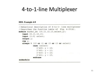
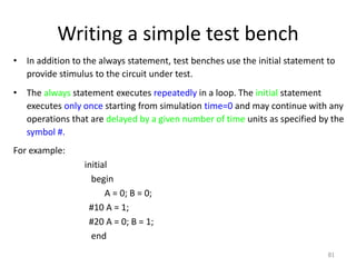
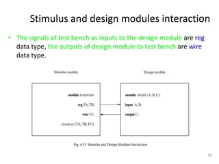
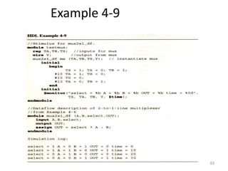
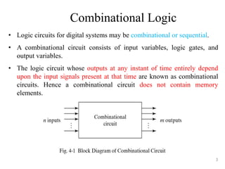
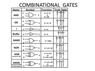
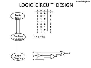
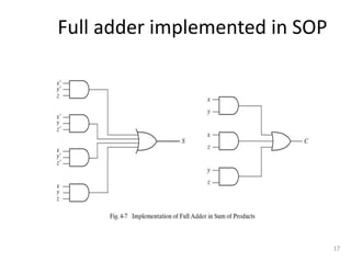
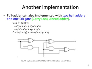
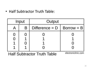
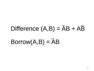
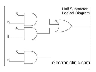
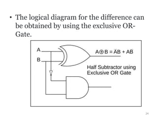
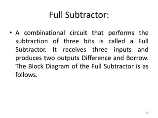
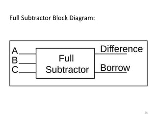
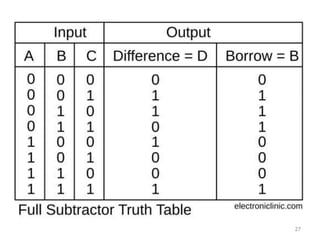
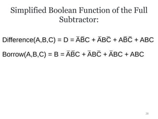
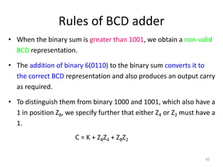
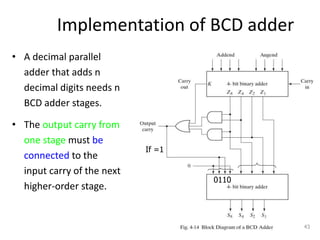
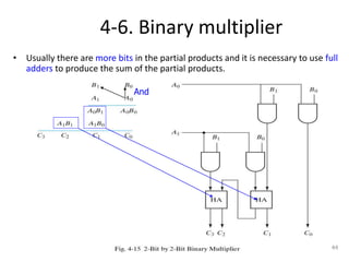
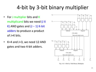
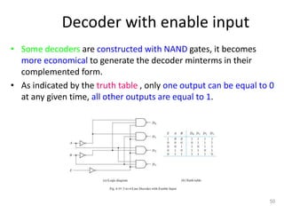
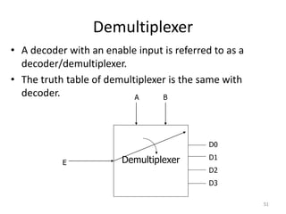
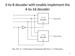
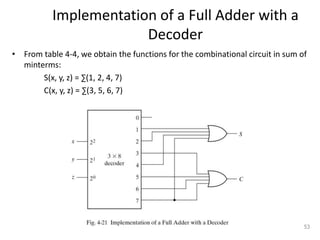
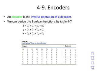
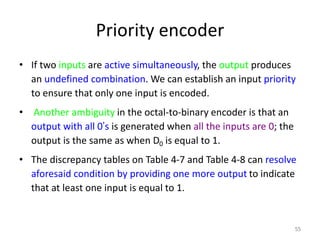
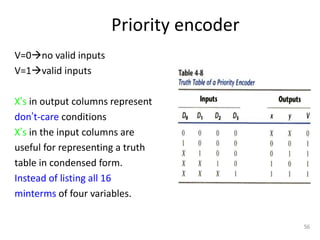
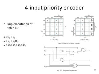
The document discusses combinational logic circuits including decoders, encoders, multiplexers, demultiplexers, adders, subtractors, and magnitude comparators. It provides details on their design procedures, truth tables, logic diagrams, and implementations using basic logic gates. Combinational logic circuits have outputs that depend only on the current inputs and do not have memory elements.

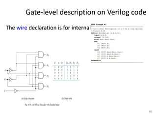
![Dataflow description of 4-bit adder
75
HDL Example 4-4
//Dataflow description of 4-bit adder
module binary_adder (A,B,Cin,SUM,Cout);
input [3:0] A,B;
input Cin;
output [3:0] SUM;
output Cout;
assign {Cout,SUM} = A + B +Cin;
endmodule](https://image.slidesharecdn.com/combinational-circuit1-231017040041-0bbf5c72/85/combinational-circuit-1-ppt-75-320.jpg)