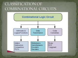
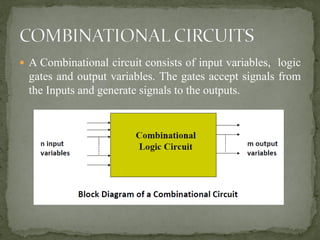
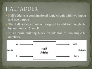
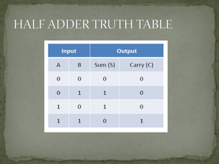
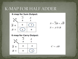
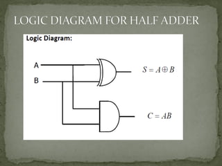
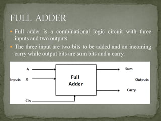
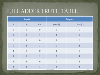
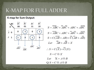
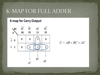
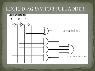
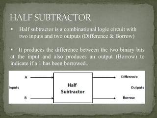
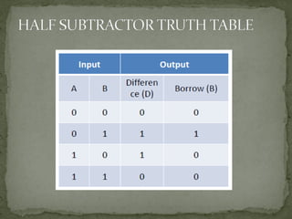
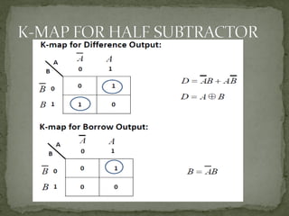
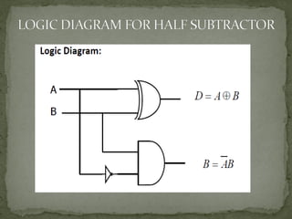
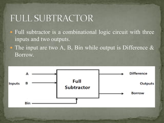
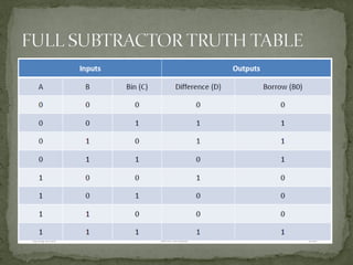
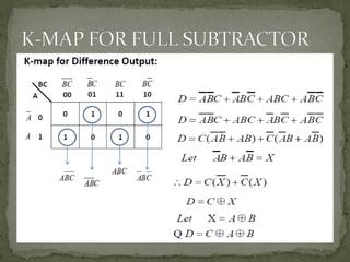
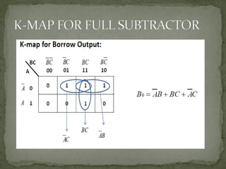
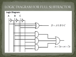
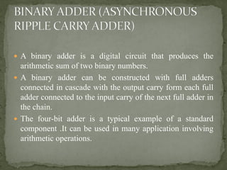
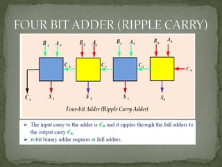
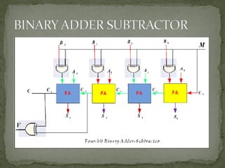
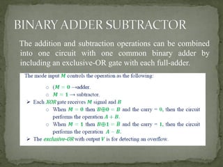
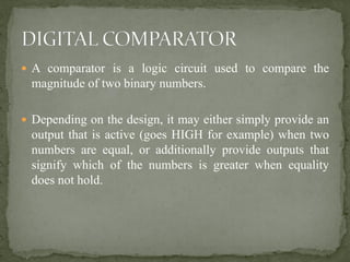
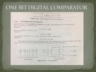
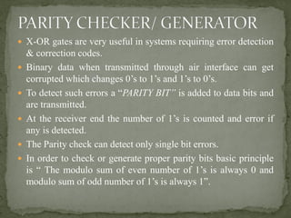
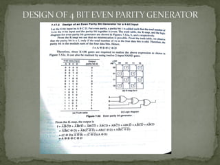
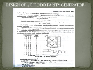
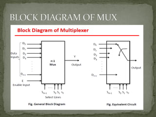
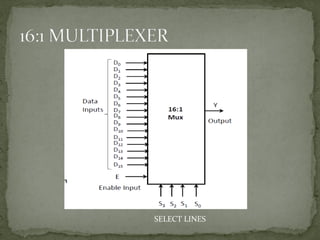
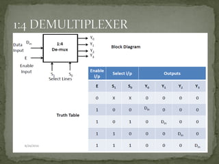
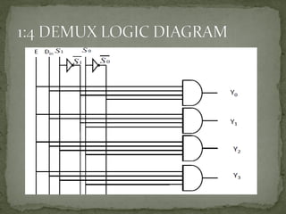
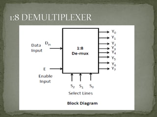
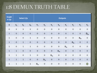
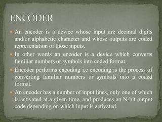
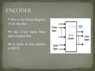
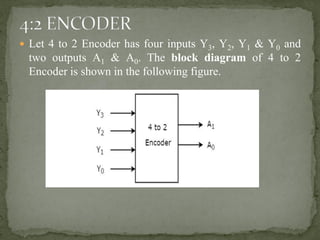
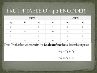
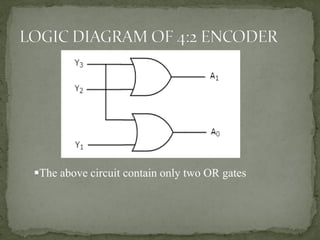
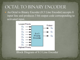
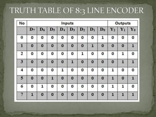
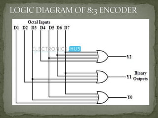
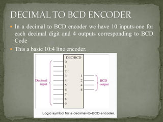
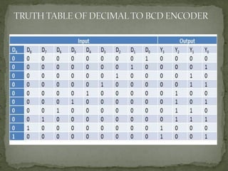
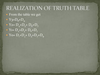
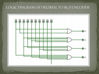
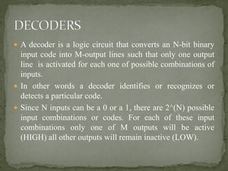
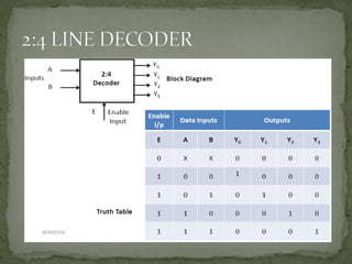
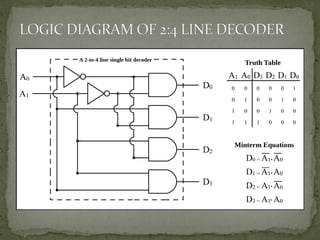
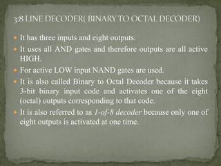
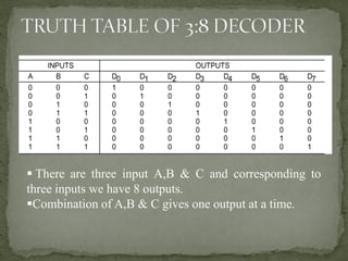
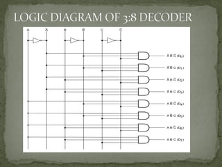
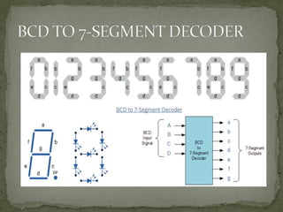
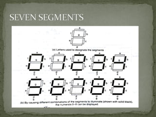
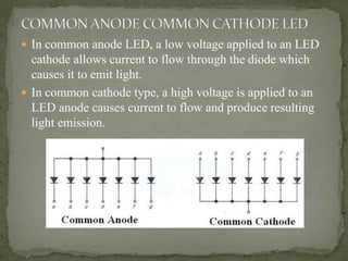
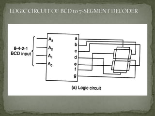
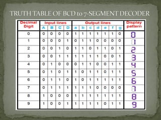
SlideShare a Scribd company logo
PREPARED
BY
NABARUN CHAKRABORTY
Assistant Professor
BARAK VALLEY ENGINEERING COLLEGE
KARIMGANJ, ASSAM
 Digital Circuits- Combinational & Sequential
 Classification of Combinational Circuits
 Arithmetic Circuits- Half Adder/Full Adder, Half
Subtractor/ Full Subtractor.
 Binary Adder (Asynchronous Ripple- Carry Adder)
 Binary Adder Subtractor
 Digital Comparator
 Parity Checker/Generator
 Multiplexer & Demultiplexer
 Encoder & Decoder.
 BCD to 7-Segment Decoders.
 Combinational circuit consists of logic gates whose outputs
at any time are determined directly from the present
combination of inputs without regard to previous inputs.
 Sequential Circuit employ memory elements in addition to
logic gates. Their outputs are a function of the inputs and
the state of the memory elements.
 A Combinational circuit consists of input variables, logic
gates and output variables. The gates accept signals from
the Inputs and generate signals to the outputs.
 Minimum no. of gates.
 Minimum no. of inputs to the gates.
 Minimum propagation time of the signal through the
circuit.
 Minimum no. of interconnections and
 Limitations of the driving capabilities of each gate.
 Half adder is a combinational logic circuit with two inputs
and two outputs.
 The half adder circuit is designed to add two single bit
binary number A and B.
 It is a basic building block for addition of two single bit
numbers.
 Full adder is a combinational logic circuit with three
inputs and two outputs.
 The three input are two bits to be added and an incoming
carry while output bits are sum bits and a carry.
▪ Half subtractor is a combinational logic circuit with
two inputs and two outputs (Difference & Borrow)
▪ It produces the difference between the two binary bits
at the input and also produces an output (Borrow) to
indicate if a 1 has been borrowed..
 Full subtractor is a combinational logic circuit with three
inputs and two outputs.
 The input are two A, B, Bin while output is Difference &
Borrow.
 A binary adder is a digital circuit that produces the
arithmetic sum of two binary numbers.
 A binary adder can be constructed with full adders
connected in cascade with the output carry form each full
adder connected to the input carry of the next full adder in
the chain.
 The four-bit adder is a typical example of a standard
component .It can be used in many application involving
arithmetic operations.
The addition and subtraction operations can be combined
into one circuit with one common binary adder by
including an exclusive-OR gate with each full-adder.
 A comparator is a logic circuit used to compare the
magnitude of two binary numbers.
 Depending on the design, it may either simply provide an
output that is active (goes HIGH for example) when two
numbers are equal, or additionally provide outputs that
signify which of the numbers is greater when equality
does not hold.
 X-OR gates are very useful in systems requiring error detection
& correction codes.
 Binary data when transmitted through air interface can get
corrupted which changes 0’s to 1’s and 1’s to 0’s.
 To detect such errors a “PARITY BIT” is added to data bits and
are transmitted.
 At the receiver end the number of 1’s is counted and error if
any is detected.
 The Parity check can detect only single bit errors.
 In order to check or generate proper parity bits basic principle
is “ The modulo sum of even number of 1’s is always 0 and
modulo sum of odd number of 1’s is always 1”.
 Multiplexer is a special type of combinational circuit
which has a number of inputs but only one output.
 Multiplexer is a circuit which transmits large number of
information signals over a single line.
 Multiplexer is also known as “Data Selector” or MUX.
 In most of the electronic systems, the digital data is
available on more than one lines. It is necessary to route
this data over a single line. Under such circumstances we
require a circuit which select one of the many inputs at a
time and the circuit is MULTIPLXER.
▪ There is also an Enable Input which when “0” the
MUX is in OFF state and when “1” is in ON state.
 In a 8:1 MUX, there are 3 select lines to choose from a
total combination of 8 input lines and by means of 3 select
lines one combination can be chosen at a time.
 We need three (3) select lines because 2^(3)=8 and 8
combinations of input can easily be handled by using 3
select lines.
 Moreover we also have a Enable Input, which should
mandatorily be at Logic 1 i.e HIGH (or in electrical terms
it should have 5V or 15V)
SELECT LINES
SELECT LINES
 It reduces the number of wires.
 So it reduces the circuit complexity and cost.
 We can implement many combinational circuits using
MULTIPLEXER.
 It simplifies the logic design.
 It does not need the k-map and simplification
 It is used as a data selector to select one out of many data
inputs.
 It is used for simplification of logic design.
 It is used in data acquisition system.
 In designing the combinational circuits.
 In Digital to Analog converters.
 To minimize the number of connections.
 A de-multiplexer performs the reverse operation of a
multiplexer i.e. it receives one input and distributes it over
several outputs.
 At a time only one output line is selected by the select
lines and the input is transmitted to the selected output
line.
 It has only one input line, n number of output lines and m
number of select lines.
 An encoder is a device whose input are decimal digits
and/or alphabetic character and whose outputs are coded
representation of those inputs.
 In other words an encoder is a device which converts
familiar numbers or symbols into coded format.
 Encoder performs encoding i.e encoding is the process of
converting familiar numbers or symbols into a coded
format.
 An encoder has a number of input lines, only one of which
is activated at a given time, and produces an N-bit output
code depending on which input is activated.
▪ This is the block diagram
of an encoder.
▪It has 2^(n) input lines
and n output line.
▪It is more or less similar
to MUX.
 Let 4 to 2 Encoder has four inputs Y3, Y2, Y1 & Y0 and
two outputs A1 & A0. The block diagram of 4 to 2
Encoder is shown in the following figure.
▪The above circuit contain only two OR gates
 An Octal to Binary Encoder (8:3 Line Encoder) accepts 8
input line and produces 3 bit output code corresponding to
activated input.
Block Diagram of 8:3 Line Encoder
 In a decimal to BCD encoder we have 10 inputs-one for
each decimal digit and 4 outputs corresponding to BCD
Code
 This a basic 10:4 line encoder.
 From the table we get
 Y3=D8+D9
 Y2= D4+D5+ D6+D7
 Y1= D2+D3+ D6+D7
 Y0= D1+D3+ D5+D7+D9
 A decoder is a logic circuit that converts an N-bit binary
input code into M-output lines such that only one output
line is activated for each one of possible combinations of
inputs.
 In other words a decoder identifies or recognizes or
detects a particular code.
 Since N inputs can be a 0 or a 1, there are 2^(N) possible
input combinations or codes. For each of these input
combinations only one of M outputs will be active
(HIGH) all other outputs will remain inactive (LOW).
 It has three inputs and eight outputs.
 It uses all AND gates and therefore outputs are all active
HIGH.
 For active LOW input NAND gates are used.
 It is also called Binary to Octal Decoder because it takes
3-bit binary input code and activates one of the eight
(octal) outputs corresponding to that code.
 It is also referred to as 1-of-8 decoder because only one of
eight outputs is activated at one time.
▪ There are three input A,B & C and corresponding to
three inputs we have 8 outputs.
▪Combination of A,B & C gives one output at a time.
 This type of decoder accepts the BCD Code and provides
outputs to energize seven segment display devices in order
to produce a decimal read out.
 Sometimes HEX Characters A-F may also be produced.
 Each segment is made up of material that emits light when
current flows through it.
 Common examples are LED’s, Incandescent Filaments
and LCD’s.
 The seven segment display has seven light emitting
segments.
 In common anode LED, a low voltage applied to an LED
cathode allows current to flow through the diode which
causes it to emit light.
 In common cathode type, a high voltage is applied to an
LED anode causes current to flow and produce resulting
light emission.
Combinational circuits

More Related Content

What's hot

Arithmetic and logic unit
Arithmetic and logic unitArithmetic and logic unit
Arithmetic and logic unit
IndrajaMeghavathula
 
Computer architecture input output organization
Computer architecture input output organizationComputer architecture input output organization
Computer architecture input output organization
Mazin Alwaaly
 
BOOLEAN ALGEBRA AND LOGIC GATE
BOOLEAN ALGEBRA AND LOGIC GATE BOOLEAN ALGEBRA AND LOGIC GATE
BOOLEAN ALGEBRA AND LOGIC GATE
Tamim Tanvir
 
1.ripple carry adder, full adder implementation using half adder.
1.ripple carry adder, full adder implementation using half adder.1.ripple carry adder, full adder implementation using half adder.
1.ripple carry adder, full adder implementation using half adder.
MdFazleRabbi18
 
Input Output Organization
Input Output OrganizationInput Output Organization
Input Output Organization
Kamal Acharya
 
decoder and encoder
 decoder and encoder decoder and encoder
decoder and encoder
Unsa Shakir
 
multiplexers and demultiplexers
 multiplexers and demultiplexers multiplexers and demultiplexers
multiplexers and demultiplexers
Unsa Shakir
 
Multiplexers
MultiplexersMultiplexers
Multiplexers
DrSonali Vyas
 
Register transfer language & its micro operations
Register transfer language & its micro operationsRegister transfer language & its micro operations
Register transfer language & its micro operations
Lakshya Sharma
 
Combinational Circuits & Sequential Circuits
Combinational Circuits & Sequential CircuitsCombinational Circuits & Sequential Circuits
Combinational Circuits & Sequential Circuits
gourav kottawar
 
Latches and flip flop
Latches and flip flopLatches and flip flop
Latches and flip flop
Shuaib Hotak
 
Boolean algebra & logic gates
Boolean algebra & logic gatesBoolean algebra & logic gates
Boolean algebra & logic gates
Prof. Dr. K. Adisesha
 
carry look ahead adder
carry look ahead addercarry look ahead adder
carry look ahead adder
ASHISH MANI
 
Combinational circuits
Combinational circuits Combinational circuits
Combinational circuits
DrSonali Vyas
 
Programmable logic devices
Programmable logic devicesProgrammable logic devices
Programmable logic devices
ISMT College
 
Carry look ahead adder
Carry look ahead adderCarry look ahead adder
Carry look ahead adder
dragonpradeep
 
Computer architecture control unit
Computer architecture control unitComputer architecture control unit
Computer architecture control unit
Mazin Alwaaly
 
Decoders-Digital Electronics
Decoders-Digital ElectronicsDecoders-Digital Electronics
Decoders-Digital Electronics
Paurav Shah
 
Arithmetic Logic Unit (ALU)
Arithmetic Logic Unit (ALU)Arithmetic Logic Unit (ALU)
Arithmetic Logic Unit (ALU)
Student
 
8086 microprocessor-architecture
8086 microprocessor-architecture8086 microprocessor-architecture
8086 microprocessor-architecture
prasadpawaskar
 

What's hot (20)

Arithmetic and logic unit
Arithmetic and logic unitArithmetic and logic unit
Arithmetic and logic unit
 
Computer architecture input output organization
Computer architecture input output organizationComputer architecture input output organization
Computer architecture input output organization
 
BOOLEAN ALGEBRA AND LOGIC GATE
BOOLEAN ALGEBRA AND LOGIC GATE BOOLEAN ALGEBRA AND LOGIC GATE
BOOLEAN ALGEBRA AND LOGIC GATE
 
1.ripple carry adder, full adder implementation using half adder.
1.ripple carry adder, full adder implementation using half adder.1.ripple carry adder, full adder implementation using half adder.
1.ripple carry adder, full adder implementation using half adder.
 
Input Output Organization
Input Output OrganizationInput Output Organization
Input Output Organization
 
decoder and encoder
 decoder and encoder decoder and encoder
decoder and encoder
 
multiplexers and demultiplexers
 multiplexers and demultiplexers multiplexers and demultiplexers
multiplexers and demultiplexers
 
Multiplexers
MultiplexersMultiplexers
Multiplexers
 
Register transfer language & its micro operations
Register transfer language & its micro operationsRegister transfer language & its micro operations
Register transfer language & its micro operations
 
Combinational Circuits & Sequential Circuits
Combinational Circuits & Sequential CircuitsCombinational Circuits & Sequential Circuits
Combinational Circuits & Sequential Circuits
 
Latches and flip flop
Latches and flip flopLatches and flip flop
Latches and flip flop
 
Boolean algebra & logic gates
Boolean algebra & logic gatesBoolean algebra & logic gates
Boolean algebra & logic gates
 
carry look ahead adder
carry look ahead addercarry look ahead adder
carry look ahead adder
 
Combinational circuits
Combinational circuits Combinational circuits
Combinational circuits
 
Programmable logic devices
Programmable logic devicesProgrammable logic devices
Programmable logic devices
 
Carry look ahead adder
Carry look ahead adderCarry look ahead adder
Carry look ahead adder
 
Computer architecture control unit
Computer architecture control unitComputer architecture control unit
Computer architecture control unit
 
Decoders-Digital Electronics
Decoders-Digital ElectronicsDecoders-Digital Electronics
Decoders-Digital Electronics
 
Arithmetic Logic Unit (ALU)
Arithmetic Logic Unit (ALU)Arithmetic Logic Unit (ALU)
Arithmetic Logic Unit (ALU)
 
8086 microprocessor-architecture
8086 microprocessor-architecture8086 microprocessor-architecture
8086 microprocessor-architecture
 

Similar to Combinational circuits

CHAPTER 6: Function of Combination Logic From Flyod ( Digital Logic Design )
CHAPTER 6: Function of Combination Logic From Flyod ( Digital Logic Design ) CHAPTER 6: Function of Combination Logic From Flyod ( Digital Logic Design )
CHAPTER 6: Function of Combination Logic From Flyod ( Digital Logic Design )
Sefat Ahammed Shovo
 
B sc3 unit 4 combi..lckt
B sc3 unit 4 combi..lcktB sc3 unit 4 combi..lckt
B sc3 unit 4 combi..lckt
MahiboobAliMulla
 
STLD-Combinational logic design
STLD-Combinational  logic design STLD-Combinational  logic design
STLD-Combinational logic design
Abhinay Potlabathini
 
FYBSC IT Digital Electronics Unit IV Chapter I Multiplexer, Demultiplexer, AL...
FYBSC IT Digital Electronics Unit IV Chapter I Multiplexer, Demultiplexer, AL...FYBSC IT Digital Electronics Unit IV Chapter I Multiplexer, Demultiplexer, AL...
FYBSC IT Digital Electronics Unit IV Chapter I Multiplexer, Demultiplexer, AL...
Arti Parab Academics
 
Combinational circuit
Combinational circuitCombinational circuit
Combinational circuit
SIVALAKSHMIPANNEERSE
 
Cs302 shortnoteslectures1to45
Cs302 shortnoteslectures1to45Cs302 shortnoteslectures1to45
Cs302 shortnoteslectures1to45
javediqbalmirza
 
Interfacing of data converters & io devices
Interfacing of data converters & io devicesInterfacing of data converters & io devices
Interfacing of data converters & io devices
Dr.YNM
 
Digital Electronics-Unit II.pdf
Digital Electronics-Unit II.pdfDigital Electronics-Unit II.pdf
Digital Electronics-Unit II.pdf
Kannan Kanagaraj
 
Digital electronics nandhini kusuma
Digital electronics nandhini kusumaDigital electronics nandhini kusuma
Digital electronics nandhini kusuma
kusuma11
 
Digital electronics nandhini kusuma
Digital electronics nandhini kusumaDigital electronics nandhini kusuma
Digital electronics nandhini kusuma
kusuma11
 
Digital electronics nandhini kusuma
Digital electronics nandhini kusumaDigital electronics nandhini kusuma
Digital electronics nandhini kusuma
kusuma11
 
ATT SMK.pptx
ATT SMK.pptxATT SMK.pptx
ATT SMK.pptx
MadhavKarve
 
SESSION 2.ppt
SESSION 2.pptSESSION 2.ppt
SESSION 2.ppt
Saranya S
 
DLD Lecture No 22 Decoder Circuit and Types of Decoder.pptx
DLD Lecture No 22 Decoder Circuit and Types of Decoder.pptxDLD Lecture No 22 Decoder Circuit and Types of Decoder.pptx
DLD Lecture No 22 Decoder Circuit and Types of Decoder.pptx
SaveraAyub2
 
2 marks DPCO.pdf
2 marks DPCO.pdf2 marks DPCO.pdf
2 marks DPCO.pdf
Vhhvf
 
Lect 1 unit 2.pdf
Lect 1 unit 2.pdfLect 1 unit 2.pdf
Lect 1 unit 2.pdf
saijalvishwakarma12
 
DCF-Combinational circuit
DCF-Combinational circuitDCF-Combinational circuit
DCF-Combinational circuit
vinothinisureshbabu
 
Digital Logic Design
Digital Logic Design Digital Logic Design
Digital Logic Design
Vaagdevi College of Engineering
 
Computer Organization And Architecture lab manual
Computer Organization And Architecture lab manualComputer Organization And Architecture lab manual
Computer Organization And Architecture lab manual
Nitesh Dubey
 
presentation.pptx
presentation.pptxpresentation.pptx
presentation.pptx
MuhammadSalman585
 

Similar to Combinational circuits (20)

CHAPTER 6: Function of Combination Logic From Flyod ( Digital Logic Design )
CHAPTER 6: Function of Combination Logic From Flyod ( Digital Logic Design ) CHAPTER 6: Function of Combination Logic From Flyod ( Digital Logic Design )
CHAPTER 6: Function of Combination Logic From Flyod ( Digital Logic Design )
 
B sc3 unit 4 combi..lckt
B sc3 unit 4 combi..lcktB sc3 unit 4 combi..lckt
B sc3 unit 4 combi..lckt
 
STLD-Combinational logic design
STLD-Combinational  logic design STLD-Combinational  logic design
STLD-Combinational logic design
 
FYBSC IT Digital Electronics Unit IV Chapter I Multiplexer, Demultiplexer, AL...
FYBSC IT Digital Electronics Unit IV Chapter I Multiplexer, Demultiplexer, AL...FYBSC IT Digital Electronics Unit IV Chapter I Multiplexer, Demultiplexer, AL...
FYBSC IT Digital Electronics Unit IV Chapter I Multiplexer, Demultiplexer, AL...
 
Combinational circuit
Combinational circuitCombinational circuit
Combinational circuit
 
Cs302 shortnoteslectures1to45
Cs302 shortnoteslectures1to45Cs302 shortnoteslectures1to45
Cs302 shortnoteslectures1to45
 
Interfacing of data converters & io devices
Interfacing of data converters & io devicesInterfacing of data converters & io devices
Interfacing of data converters & io devices
 
Digital Electronics-Unit II.pdf
Digital Electronics-Unit II.pdfDigital Electronics-Unit II.pdf
Digital Electronics-Unit II.pdf
 
Digital electronics nandhini kusuma
Digital electronics nandhini kusumaDigital electronics nandhini kusuma
Digital electronics nandhini kusuma
 
Digital electronics nandhini kusuma
Digital electronics nandhini kusumaDigital electronics nandhini kusuma
Digital electronics nandhini kusuma
 
Digital electronics nandhini kusuma
Digital electronics nandhini kusumaDigital electronics nandhini kusuma
Digital electronics nandhini kusuma
 
ATT SMK.pptx
ATT SMK.pptxATT SMK.pptx
ATT SMK.pptx
 
SESSION 2.ppt
SESSION 2.pptSESSION 2.ppt
SESSION 2.ppt
 
DLD Lecture No 22 Decoder Circuit and Types of Decoder.pptx
DLD Lecture No 22 Decoder Circuit and Types of Decoder.pptxDLD Lecture No 22 Decoder Circuit and Types of Decoder.pptx
DLD Lecture No 22 Decoder Circuit and Types of Decoder.pptx
 
2 marks DPCO.pdf
2 marks DPCO.pdf2 marks DPCO.pdf
2 marks DPCO.pdf
 
Lect 1 unit 2.pdf
Lect 1 unit 2.pdfLect 1 unit 2.pdf
Lect 1 unit 2.pdf
 
DCF-Combinational circuit
DCF-Combinational circuitDCF-Combinational circuit
DCF-Combinational circuit
 
Digital Logic Design
Digital Logic Design Digital Logic Design
Digital Logic Design
 
Computer Organization And Architecture lab manual
Computer Organization And Architecture lab manualComputer Organization And Architecture lab manual
Computer Organization And Architecture lab manual
 
presentation.pptx
presentation.pptxpresentation.pptx
presentation.pptx
 

Recently uploaded

road safety engineering r s e unit 3.pdf
road safety engineering  r s e unit 3.pdfroad safety engineering  r s e unit 3.pdf
road safety engineering r s e unit 3.pdf
VENKATESHvenky89705
 
The Benefits and Techniques of Trenchless Pipe Repair.pdf
The Benefits and Techniques of Trenchless Pipe Repair.pdfThe Benefits and Techniques of Trenchless Pipe Repair.pdf
The Benefits and Techniques of Trenchless Pipe Repair.pdf
Pipe Restoration Solutions
 
AKS UNIVERSITY Satna Final Year Project By OM Hardaha.pdf
AKS UNIVERSITY Satna Final Year Project By OM Hardaha.pdfAKS UNIVERSITY Satna Final Year Project By OM Hardaha.pdf
AKS UNIVERSITY Satna Final Year Project By OM Hardaha.pdf
SamSarthak3
 
Pile Foundation by Venkatesh Taduvai (Sub Geotechnical Engineering II)-conver...
Pile Foundation by Venkatesh Taduvai (Sub Geotechnical Engineering II)-conver...Pile Foundation by Venkatesh Taduvai (Sub Geotechnical Engineering II)-conver...
Pile Foundation by Venkatesh Taduvai (Sub Geotechnical Engineering II)-conver...
AJAYKUMARPUND1
 
Event Management System Vb Net Project Report.pdf
Event Management System Vb Net  Project Report.pdfEvent Management System Vb Net  Project Report.pdf
Event Management System Vb Net Project Report.pdf
Kamal Acharya
 
DESIGN A COTTON SEED SEPARATION MACHINE.docx
DESIGN A COTTON SEED SEPARATION MACHINE.docxDESIGN A COTTON SEED SEPARATION MACHINE.docx
DESIGN A COTTON SEED SEPARATION MACHINE.docx
FluxPrime1
 
Hybrid optimization of pumped hydro system and solar- Engr. Abdul-Azeez.pdf
Hybrid optimization of pumped hydro system and solar- Engr. Abdul-Azeez.pdfHybrid optimization of pumped hydro system and solar- Engr. Abdul-Azeez.pdf
Hybrid optimization of pumped hydro system and solar- Engr. Abdul-Azeez.pdf
fxintegritypublishin
 
block diagram and signal flow graph representation
block diagram and signal flow graph representationblock diagram and signal flow graph representation
block diagram and signal flow graph representation
Divya Somashekar
 
COLLEGE BUS MANAGEMENT SYSTEM PROJECT REPORT.pdf
COLLEGE BUS MANAGEMENT SYSTEM PROJECT REPORT.pdfCOLLEGE BUS MANAGEMENT SYSTEM PROJECT REPORT.pdf
COLLEGE BUS MANAGEMENT SYSTEM PROJECT REPORT.pdf
Kamal Acharya
 
Design and Analysis of Algorithms-DP,Backtracking,Graphs,B&B
Design and Analysis of Algorithms-DP,Backtracking,Graphs,B&BDesign and Analysis of Algorithms-DP,Backtracking,Graphs,B&B
Design and Analysis of Algorithms-DP,Backtracking,Graphs,B&B
Sreedhar Chowdam
 
Forklift Classes Overview by Intella Parts
Forklift Classes Overview by Intella PartsForklift Classes Overview by Intella Parts
Forklift Classes Overview by Intella Parts
Intella Parts
 
ethical hacking in wireless-hacking1.ppt
ethical hacking in wireless-hacking1.pptethical hacking in wireless-hacking1.ppt
ethical hacking in wireless-hacking1.ppt
Jayaprasanna4
 
Gen AI Study Jams _ For the GDSC Leads in India.pdf
Gen AI Study Jams _ For the GDSC Leads in India.pdfGen AI Study Jams _ For the GDSC Leads in India.pdf
Gen AI Study Jams _ For the GDSC Leads in India.pdf
gdsczhcet
 
LIGA(E)11111111111111111111111111111111111111111.ppt
LIGA(E)11111111111111111111111111111111111111111.pptLIGA(E)11111111111111111111111111111111111111111.ppt
LIGA(E)11111111111111111111111111111111111111111.ppt
ssuser9bd3ba
 
一比一原版(SFU毕业证)西蒙菲莎大学毕业证成绩单如何办理
一比一原版(SFU毕业证)西蒙菲莎大学毕业证成绩单如何办理一比一原版(SFU毕业证)西蒙菲莎大学毕业证成绩单如何办理
一比一原版(SFU毕业证)西蒙菲莎大学毕业证成绩单如何办理
bakpo1
 
Water Industry Process Automation and Control Monthly - May 2024.pdf
Water Industry Process Automation and Control Monthly - May 2024.pdfWater Industry Process Automation and Control Monthly - May 2024.pdf
Water Industry Process Automation and Control Monthly - May 2024.pdf
Water Industry Process Automation & Control
 
Immunizing Image Classifiers Against Localized Adversary Attacks
Immunizing Image Classifiers Against Localized Adversary AttacksImmunizing Image Classifiers Against Localized Adversary Attacks
Immunizing Image Classifiers Against Localized Adversary Attacks
gerogepatton
 
Sachpazis:Terzaghi Bearing Capacity Estimation in simple terms with Calculati...
Sachpazis:Terzaghi Bearing Capacity Estimation in simple terms with Calculati...Sachpazis:Terzaghi Bearing Capacity Estimation in simple terms with Calculati...
Sachpazis:Terzaghi Bearing Capacity Estimation in simple terms with Calculati...
Dr.Costas Sachpazis
 
Vaccine management system project report documentation..pdf
Vaccine management system project report documentation..pdfVaccine management system project report documentation..pdf
Vaccine management system project report documentation..pdf
Kamal Acharya
 
Automobile Management System Project Report.pdf
Automobile Management System Project Report.pdfAutomobile Management System Project Report.pdf
Automobile Management System Project Report.pdf
Kamal Acharya
 

Recently uploaded (20)

road safety engineering r s e unit 3.pdf
road safety engineering  r s e unit 3.pdfroad safety engineering  r s e unit 3.pdf
road safety engineering r s e unit 3.pdf
 
The Benefits and Techniques of Trenchless Pipe Repair.pdf
The Benefits and Techniques of Trenchless Pipe Repair.pdfThe Benefits and Techniques of Trenchless Pipe Repair.pdf
The Benefits and Techniques of Trenchless Pipe Repair.pdf
 
AKS UNIVERSITY Satna Final Year Project By OM Hardaha.pdf
AKS UNIVERSITY Satna Final Year Project By OM Hardaha.pdfAKS UNIVERSITY Satna Final Year Project By OM Hardaha.pdf
AKS UNIVERSITY Satna Final Year Project By OM Hardaha.pdf
 
Pile Foundation by Venkatesh Taduvai (Sub Geotechnical Engineering II)-conver...
Pile Foundation by Venkatesh Taduvai (Sub Geotechnical Engineering II)-conver...Pile Foundation by Venkatesh Taduvai (Sub Geotechnical Engineering II)-conver...
Pile Foundation by Venkatesh Taduvai (Sub Geotechnical Engineering II)-conver...
 
Event Management System Vb Net Project Report.pdf
Event Management System Vb Net  Project Report.pdfEvent Management System Vb Net  Project Report.pdf
Event Management System Vb Net Project Report.pdf
 
DESIGN A COTTON SEED SEPARATION MACHINE.docx
DESIGN A COTTON SEED SEPARATION MACHINE.docxDESIGN A COTTON SEED SEPARATION MACHINE.docx
DESIGN A COTTON SEED SEPARATION MACHINE.docx
 
Hybrid optimization of pumped hydro system and solar- Engr. Abdul-Azeez.pdf
Hybrid optimization of pumped hydro system and solar- Engr. Abdul-Azeez.pdfHybrid optimization of pumped hydro system and solar- Engr. Abdul-Azeez.pdf
Hybrid optimization of pumped hydro system and solar- Engr. Abdul-Azeez.pdf
 
block diagram and signal flow graph representation
block diagram and signal flow graph representationblock diagram and signal flow graph representation
block diagram and signal flow graph representation
 
COLLEGE BUS MANAGEMENT SYSTEM PROJECT REPORT.pdf
COLLEGE BUS MANAGEMENT SYSTEM PROJECT REPORT.pdfCOLLEGE BUS MANAGEMENT SYSTEM PROJECT REPORT.pdf
COLLEGE BUS MANAGEMENT SYSTEM PROJECT REPORT.pdf
 
Design and Analysis of Algorithms-DP,Backtracking,Graphs,B&B
Design and Analysis of Algorithms-DP,Backtracking,Graphs,B&BDesign and Analysis of Algorithms-DP,Backtracking,Graphs,B&B
Design and Analysis of Algorithms-DP,Backtracking,Graphs,B&B
 
Forklift Classes Overview by Intella Parts
Forklift Classes Overview by Intella PartsForklift Classes Overview by Intella Parts
Forklift Classes Overview by Intella Parts
 
ethical hacking in wireless-hacking1.ppt
ethical hacking in wireless-hacking1.pptethical hacking in wireless-hacking1.ppt
ethical hacking in wireless-hacking1.ppt
 
Gen AI Study Jams _ For the GDSC Leads in India.pdf
Gen AI Study Jams _ For the GDSC Leads in India.pdfGen AI Study Jams _ For the GDSC Leads in India.pdf
Gen AI Study Jams _ For the GDSC Leads in India.pdf
 
LIGA(E)11111111111111111111111111111111111111111.ppt
LIGA(E)11111111111111111111111111111111111111111.pptLIGA(E)11111111111111111111111111111111111111111.ppt
LIGA(E)11111111111111111111111111111111111111111.ppt
 
一比一原版(SFU毕业证)西蒙菲莎大学毕业证成绩单如何办理
一比一原版(SFU毕业证)西蒙菲莎大学毕业证成绩单如何办理一比一原版(SFU毕业证)西蒙菲莎大学毕业证成绩单如何办理
一比一原版(SFU毕业证)西蒙菲莎大学毕业证成绩单如何办理
 
Water Industry Process Automation and Control Monthly - May 2024.pdf
Water Industry Process Automation and Control Monthly - May 2024.pdfWater Industry Process Automation and Control Monthly - May 2024.pdf
Water Industry Process Automation and Control Monthly - May 2024.pdf
 
Immunizing Image Classifiers Against Localized Adversary Attacks
Immunizing Image Classifiers Against Localized Adversary AttacksImmunizing Image Classifiers Against Localized Adversary Attacks
Immunizing Image Classifiers Against Localized Adversary Attacks
 
Sachpazis:Terzaghi Bearing Capacity Estimation in simple terms with Calculati...
Sachpazis:Terzaghi Bearing Capacity Estimation in simple terms with Calculati...Sachpazis:Terzaghi Bearing Capacity Estimation in simple terms with Calculati...
Sachpazis:Terzaghi Bearing Capacity Estimation in simple terms with Calculati...
 
Vaccine management system project report documentation..pdf
Vaccine management system project report documentation..pdfVaccine management system project report documentation..pdf
Vaccine management system project report documentation..pdf
 
Automobile Management System Project Report.pdf
Automobile Management System Project Report.pdfAutomobile Management System Project Report.pdf
Automobile Management System Project Report.pdf
 

Combinational circuits

  • 1. PREPARED BY NABARUN CHAKRABORTY Assistant Professor BARAK VALLEY ENGINEERING COLLEGE KARIMGANJ, ASSAM
  • 2.  Digital Circuits- Combinational & Sequential  Classification of Combinational Circuits  Arithmetic Circuits- Half Adder/Full Adder, Half Subtractor/ Full Subtractor.  Binary Adder (Asynchronous Ripple- Carry Adder)  Binary Adder Subtractor  Digital Comparator  Parity Checker/Generator  Multiplexer & Demultiplexer  Encoder & Decoder.  BCD to 7-Segment Decoders.
  • 3.  Combinational circuit consists of logic gates whose outputs at any time are determined directly from the present combination of inputs without regard to previous inputs.  Sequential Circuit employ memory elements in addition to logic gates. Their outputs are a function of the inputs and the state of the memory elements.
  • 4.
  • 5.  A Combinational circuit consists of input variables, logic gates and output variables. The gates accept signals from the Inputs and generate signals to the outputs.
  • 6.  Minimum no. of gates.  Minimum no. of inputs to the gates.  Minimum propagation time of the signal through the circuit.  Minimum no. of interconnections and  Limitations of the driving capabilities of each gate.
  • 7.  Half adder is a combinational logic circuit with two inputs and two outputs.  The half adder circuit is designed to add two single bit binary number A and B.  It is a basic building block for addition of two single bit numbers.
  • 8.
  • 9.
  • 10.
  • 11.  Full adder is a combinational logic circuit with three inputs and two outputs.  The three input are two bits to be added and an incoming carry while output bits are sum bits and a carry.
  • 12.
  • 13.
  • 14.
  • 15.
  • 16. ▪ Half subtractor is a combinational logic circuit with two inputs and two outputs (Difference & Borrow) ▪ It produces the difference between the two binary bits at the input and also produces an output (Borrow) to indicate if a 1 has been borrowed..
  • 17.
  • 18.
  • 19.
  • 20.  Full subtractor is a combinational logic circuit with three inputs and two outputs.  The input are two A, B, Bin while output is Difference & Borrow.
  • 21.
  • 22.
  • 23.
  • 24.
  • 25.  A binary adder is a digital circuit that produces the arithmetic sum of two binary numbers.  A binary adder can be constructed with full adders connected in cascade with the output carry form each full adder connected to the input carry of the next full adder in the chain.  The four-bit adder is a typical example of a standard component .It can be used in many application involving arithmetic operations.
  • 26.
  • 27.
  • 28. The addition and subtraction operations can be combined into one circuit with one common binary adder by including an exclusive-OR gate with each full-adder.
  • 29.  A comparator is a logic circuit used to compare the magnitude of two binary numbers.  Depending on the design, it may either simply provide an output that is active (goes HIGH for example) when two numbers are equal, or additionally provide outputs that signify which of the numbers is greater when equality does not hold.
  • 30.
  • 31.  X-OR gates are very useful in systems requiring error detection & correction codes.  Binary data when transmitted through air interface can get corrupted which changes 0’s to 1’s and 1’s to 0’s.  To detect such errors a “PARITY BIT” is added to data bits and are transmitted.  At the receiver end the number of 1’s is counted and error if any is detected.  The Parity check can detect only single bit errors.  In order to check or generate proper parity bits basic principle is “ The modulo sum of even number of 1’s is always 0 and modulo sum of odd number of 1’s is always 1”.
  • 32.
  • 33.
  • 34.  Multiplexer is a special type of combinational circuit which has a number of inputs but only one output.  Multiplexer is a circuit which transmits large number of information signals over a single line.  Multiplexer is also known as “Data Selector” or MUX.  In most of the electronic systems, the digital data is available on more than one lines. It is necessary to route this data over a single line. Under such circumstances we require a circuit which select one of the many inputs at a time and the circuit is MULTIPLXER.
  • 35.
  • 36. ▪ There is also an Enable Input which when “0” the MUX is in OFF state and when “1” is in ON state.
  • 37.
  • 38.
  • 39.
  • 40.
  • 41.  In a 8:1 MUX, there are 3 select lines to choose from a total combination of 8 input lines and by means of 3 select lines one combination can be chosen at a time.  We need three (3) select lines because 2^(3)=8 and 8 combinations of input can easily be handled by using 3 select lines.  Moreover we also have a Enable Input, which should mandatorily be at Logic 1 i.e HIGH (or in electrical terms it should have 5V or 15V)
  • 43.
  • 45.  It reduces the number of wires.  So it reduces the circuit complexity and cost.  We can implement many combinational circuits using MULTIPLEXER.  It simplifies the logic design.  It does not need the k-map and simplification
  • 46.  It is used as a data selector to select one out of many data inputs.  It is used for simplification of logic design.  It is used in data acquisition system.  In designing the combinational circuits.  In Digital to Analog converters.  To minimize the number of connections.
  • 47.
  • 48.
  • 49.
  • 50.
  • 51.  A de-multiplexer performs the reverse operation of a multiplexer i.e. it receives one input and distributes it over several outputs.  At a time only one output line is selected by the select lines and the input is transmitted to the selected output line.  It has only one input line, n number of output lines and m number of select lines.
  • 52.
  • 53.
  • 54.
  • 55.
  • 56.
  • 57.
  • 58.
  • 59.
  • 60.
  • 61.
  • 62.  An encoder is a device whose input are decimal digits and/or alphabetic character and whose outputs are coded representation of those inputs.  In other words an encoder is a device which converts familiar numbers or symbols into coded format.  Encoder performs encoding i.e encoding is the process of converting familiar numbers or symbols into a coded format.  An encoder has a number of input lines, only one of which is activated at a given time, and produces an N-bit output code depending on which input is activated.
  • 63. ▪ This is the block diagram of an encoder. ▪It has 2^(n) input lines and n output line. ▪It is more or less similar to MUX.
  • 64.  Let 4 to 2 Encoder has four inputs Y3, Y2, Y1 & Y0 and two outputs A1 & A0. The block diagram of 4 to 2 Encoder is shown in the following figure.
  • 65.
  • 66. ▪The above circuit contain only two OR gates
  • 67.  An Octal to Binary Encoder (8:3 Line Encoder) accepts 8 input line and produces 3 bit output code corresponding to activated input. Block Diagram of 8:3 Line Encoder
  • 68.
  • 69.
  • 70.  In a decimal to BCD encoder we have 10 inputs-one for each decimal digit and 4 outputs corresponding to BCD Code  This a basic 10:4 line encoder.
  • 71.
  • 72.  From the table we get  Y3=D8+D9  Y2= D4+D5+ D6+D7  Y1= D2+D3+ D6+D7  Y0= D1+D3+ D5+D7+D9
  • 73.
  • 74.  A decoder is a logic circuit that converts an N-bit binary input code into M-output lines such that only one output line is activated for each one of possible combinations of inputs.  In other words a decoder identifies or recognizes or detects a particular code.  Since N inputs can be a 0 or a 1, there are 2^(N) possible input combinations or codes. For each of these input combinations only one of M outputs will be active (HIGH) all other outputs will remain inactive (LOW).
  • 75.
  • 76.
  • 77.  It has three inputs and eight outputs.  It uses all AND gates and therefore outputs are all active HIGH.  For active LOW input NAND gates are used.  It is also called Binary to Octal Decoder because it takes 3-bit binary input code and activates one of the eight (octal) outputs corresponding to that code.  It is also referred to as 1-of-8 decoder because only one of eight outputs is activated at one time.
  • 78. ▪ There are three input A,B & C and corresponding to three inputs we have 8 outputs. ▪Combination of A,B & C gives one output at a time.
  • 79.
  • 80.  This type of decoder accepts the BCD Code and provides outputs to energize seven segment display devices in order to produce a decimal read out.  Sometimes HEX Characters A-F may also be produced.  Each segment is made up of material that emits light when current flows through it.  Common examples are LED’s, Incandescent Filaments and LCD’s.  The seven segment display has seven light emitting segments.
  • 81.
  • 82.
  • 83.  In common anode LED, a low voltage applied to an LED cathode allows current to flow through the diode which causes it to emit light.  In common cathode type, a high voltage is applied to an LED anode causes current to flow and produce resulting light emission.