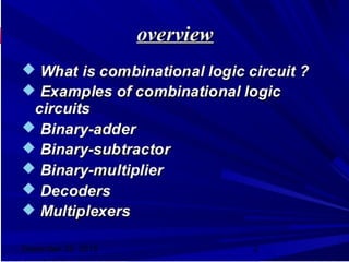
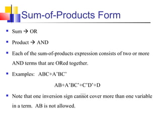
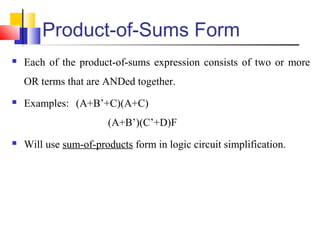
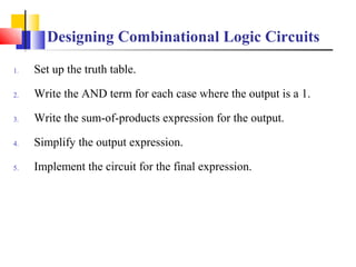
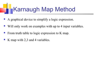
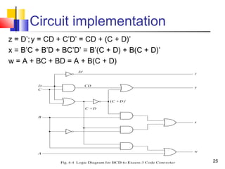
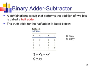
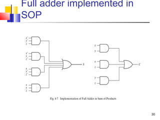
1
2
Combinational Logic
3
4
5
6
Sum-of-Products Form
 Sum  OR
 Product  AND
 Each of the sum-of-products expression consists of two or more
AND terms that are ORed together.
 Examples: ABC+A’BC’
AB+A’BC’+C’D’+D
 Note that one inversion sign cannot cover more than one variable
in a term. AB is not allowed.
Product-of-Sums Form
 Each of the product-of-sums expression consists of two or more
OR terms that are ANDed together.
 Examples: (A+B’+C)(A+C)
(A+B’)(C’+D)F
 Will use sum-of-products form in logic circuit simplification.
Simplifying Logic Circuits
Example 4.1
Circuit Simplification Methods
 Boolean algebra: greatly depends on inspiration and
experience.
 Karnaugh map: systematic, step-by-step approach.
 Pros and Cons
Algebraic Simplification
 Use the Boolean algebra theorems introduced in Chapter 3 to help
simplify the expression for a logic circuit.
 Based on experience, often becomes a trial-and-error process.
 No easy way to tell whether a simplified expression is in its
simplest form.
Designing Combinational Logic Circuits
1. Set up the truth table.
2. Write the AND term for each case where the output is a 1.
3. Write the sum-of-products expression for the output.
4. Simplify the output expression.
5. Implement the circuit for the final expression.
Example
 Design a logic circuit that is to produce a HIGH output when the
voltage (represented by a four-bit binary number ABCD) is
greater than 6V.
Example
 Generate the STOP signal and energize an indicator light
whenever either of the following conditions exists: (1) there is no
paper in the paper feeder tray; or (2) the two micro-switches in the
paper path are activated, indicating a jam.
Karnaugh Map Method
 A graphical device to simplify a logic expression.
 Will only work on examples with up to 4 input variables.
 From truth table to logic expression to K map.
 K map with 2,3 and 4 variables.
Looping
 The expression for output X can be simplified by properly
combining those squares in the K map which contain 1s. The
process of combining these 1s is called looping.
 Looping groups of two (pairs)  eliminate 1 variable
 Looping groups of four (quads)  eliminate 2 variables
 Looping groups of eight (octets) eliminate 3 variables
18
Analysis procedure
 To obtain the output Boolean functions from a logic diagram,
proceed as follows:
 Label all gate outputs that are a function of input variables with
arbitrary symbols. Determine the Boolean functions for each
gate output.
 Label the gates that are a function of input variables and
previously labeled gates with other arbitrary symbols. Find the
Boolean functions for these gates.
 Repeat the process outlined in step 2 until the outputs of the
circuit are obtained.
 By repeated substitution of previously defined functions,
obtain the output Boolean functions in terms of input variables.
19
Example
F2 = AB + AC + BC; T1 = A + B + C; T2 = ABC; T3 = F2’T1;
F1 = T3 + T2
F1 = T3 + T2 = F2’T1 + ABC = A’BC’ + A’B’C + AB’C’ + ABC
20
Derive truth table from logic diagram
Examples
 Design a combinational circuit with 3 inputs and one output.
The output is 1 if the binary value is of the input is less than 3,
Zero otherwise.
 Steps: TT, K Map, Logic Circuit
 Design a 3 I/P majority circuit
 Note:A majority circuit is a combinational circuit whose output is equal to 1
if the input variables have more 1's than 0's. The output is 0 otherwise
 Design a combinational circuit with 3 inputs X,Y,Z and 3
output A,B,C. When the binary input is 0,1,2,3 , the binary
output is one greater than the input. When the binary input is
4,5,6,7 , the binary output is one less than the input.
 Design a 4 bit 2’s Complement combinational circuit
 Design a 4 bit combinational circuit incrementer. (5 bit
output) 21
 Design a BCD to 7 Segment decoder
 I/P – 4 Bit
 O/P – a,b,c,d,e,f,g
 Design a 3 bit Binary to gray code Converter.
 Design a 4 bit gray to Binary Code Converter.
 Design a BCD to 8 4 -2 -1 code converter
22
23
Design procedure
Code-Conversion example, first, we can list the relation of the BCD
and Excess-3 codes in the truth table.
24
Karnaugh map
2. For each symbol of the Excess-3 code, we use 1’s
to draw the map for simplifying Boolean function.
25
Circuit implementation
z = D’;y = CD + C’D’ = CD + (C + D)’
x = B’C + B’D + BC’D’ = B’(C + D) + B(C + D)’
w = A + BC + BD = A + B(C + D)
26
Binary Adder-Subtractor
 A combinational circuit that performs the addition of two bits
is called a half adder.
 The truth table for the half adder is listed below:
S = x’y + xy’
C = xy
S: Sum
C: Carry
27
Implementation of Half-Adder
28
Full-Adder
 One that performs the addition of three bits(two
significant bits and a previous carry) is a full adder.
29
Simplified Expressions
S = x’y’z + x’yz’ + xy’z’ + xyz
C = xy + xz + yz
C
30
Full adder implemented in
SOP
31
Another implementation
 Full-adder can also implemented with two half
adders and one OR gate (Carry Look-Ahead
adder).
S = z ⊕ (x ⊕ y)
= z’(xy’ + x’y) + z(xy’ + x’y)’
= xy’z’ + x’yz’ + xyz + x’y’z
C = z(xy’ + x’y) + xy = xy’z + x’yz + xy
32
Binary adder
 This is also called
Ripple Carry
Adder ,because of
the construction with
full adders are
connected in
cascade.
33
Carry Propagation
 Fig.4-9 causes a unstable factor on carry bit, and produces
a longest propagation delay.
 The signal from Ci to the output carry Ci+1, propagates
through an AND and OR gates, so, for an n-bit RCA, there
are 2n gate levels for the carry to propagate from input to
output.
34
Carry Propagation
 Because the propagation delay will affect the output signals
on different time, so the signals are given enough time to get
the precise and stable outputs.
 The most widely used technique employs the principle of
carry look-ahead to improve the speed of the algorithm.
35
Boolean functions
Pi = Ai ⊕ Bi steady state value
Gi = AiBi steady state value
Output sum and carry
Si = Pi ⊕ Ci
Ci+1 = Gi + PiCi
Gi : carry generate Pi : carry propagate
C0 = input carry
C1 = G0 + P0C0
C2 = G1 + P1C1 = G1 + P1G0 + P1P0C0
C3 = G2 + P2C2 = G2 + P2G1 + P2P1G0 + P2P1P0C0
 C3 does not have to wait for C2 and C1 to propagate.
36
Logic diagram of
carry look-ahead generator
 C3 is propagated at the same time as C2 and C1.

Combinational circuit

  • 1.
  • 2.
  • 3.
  • 4.
  • 5.
  • 6.
  • 7.
    Sum-of-Products Form  Sum OR  Product  AND  Each of the sum-of-products expression consists of two or more AND terms that are ORed together.  Examples: ABC+A’BC’ AB+A’BC’+C’D’+D  Note that one inversion sign cannot cover more than one variable in a term. AB is not allowed.
  • 8.
    Product-of-Sums Form  Eachof the product-of-sums expression consists of two or more OR terms that are ANDed together.  Examples: (A+B’+C)(A+C) (A+B’)(C’+D)F  Will use sum-of-products form in logic circuit simplification.
  • 9.
  • 10.
  • 11.
    Circuit Simplification Methods Boolean algebra: greatly depends on inspiration and experience.  Karnaugh map: systematic, step-by-step approach.  Pros and Cons
  • 12.
    Algebraic Simplification  Usethe Boolean algebra theorems introduced in Chapter 3 to help simplify the expression for a logic circuit.  Based on experience, often becomes a trial-and-error process.  No easy way to tell whether a simplified expression is in its simplest form.
  • 13.
    Designing Combinational LogicCircuits 1. Set up the truth table. 2. Write the AND term for each case where the output is a 1. 3. Write the sum-of-products expression for the output. 4. Simplify the output expression. 5. Implement the circuit for the final expression.
  • 14.
    Example  Design alogic circuit that is to produce a HIGH output when the voltage (represented by a four-bit binary number ABCD) is greater than 6V.
  • 15.
    Example  Generate theSTOP signal and energize an indicator light whenever either of the following conditions exists: (1) there is no paper in the paper feeder tray; or (2) the two micro-switches in the paper path are activated, indicating a jam.
  • 16.
    Karnaugh Map Method A graphical device to simplify a logic expression.  Will only work on examples with up to 4 input variables.  From truth table to logic expression to K map.  K map with 2,3 and 4 variables.
  • 17.
    Looping  The expressionfor output X can be simplified by properly combining those squares in the K map which contain 1s. The process of combining these 1s is called looping.  Looping groups of two (pairs)  eliminate 1 variable  Looping groups of four (quads)  eliminate 2 variables  Looping groups of eight (octets) eliminate 3 variables
  • 18.
    18 Analysis procedure  Toobtain the output Boolean functions from a logic diagram, proceed as follows:  Label all gate outputs that are a function of input variables with arbitrary symbols. Determine the Boolean functions for each gate output.  Label the gates that are a function of input variables and previously labeled gates with other arbitrary symbols. Find the Boolean functions for these gates.  Repeat the process outlined in step 2 until the outputs of the circuit are obtained.  By repeated substitution of previously defined functions, obtain the output Boolean functions in terms of input variables.
  • 19.
    19 Example F2 = AB+ AC + BC; T1 = A + B + C; T2 = ABC; T3 = F2’T1; F1 = T3 + T2 F1 = T3 + T2 = F2’T1 + ABC = A’BC’ + A’B’C + AB’C’ + ABC
  • 20.
    20 Derive truth tablefrom logic diagram
  • 21.
    Examples  Design acombinational circuit with 3 inputs and one output. The output is 1 if the binary value is of the input is less than 3, Zero otherwise.  Steps: TT, K Map, Logic Circuit  Design a 3 I/P majority circuit  Note:A majority circuit is a combinational circuit whose output is equal to 1 if the input variables have more 1's than 0's. The output is 0 otherwise  Design a combinational circuit with 3 inputs X,Y,Z and 3 output A,B,C. When the binary input is 0,1,2,3 , the binary output is one greater than the input. When the binary input is 4,5,6,7 , the binary output is one less than the input.  Design a 4 bit 2’s Complement combinational circuit  Design a 4 bit combinational circuit incrementer. (5 bit output) 21
  • 22.
     Design aBCD to 7 Segment decoder  I/P – 4 Bit  O/P – a,b,c,d,e,f,g  Design a 3 bit Binary to gray code Converter.  Design a 4 bit gray to Binary Code Converter.  Design a BCD to 8 4 -2 -1 code converter 22
  • 23.
    23 Design procedure Code-Conversion example,first, we can list the relation of the BCD and Excess-3 codes in the truth table.
  • 24.
    24 Karnaugh map 2. Foreach symbol of the Excess-3 code, we use 1’s to draw the map for simplifying Boolean function.
  • 25.
    25 Circuit implementation z =D’;y = CD + C’D’ = CD + (C + D)’ x = B’C + B’D + BC’D’ = B’(C + D) + B(C + D)’ w = A + BC + BD = A + B(C + D)
  • 26.
    26 Binary Adder-Subtractor  Acombinational circuit that performs the addition of two bits is called a half adder.  The truth table for the half adder is listed below: S = x’y + xy’ C = xy S: Sum C: Carry
  • 27.
  • 28.
    28 Full-Adder  One thatperforms the addition of three bits(two significant bits and a previous carry) is a full adder.
  • 29.
    29 Simplified Expressions S =x’y’z + x’yz’ + xy’z’ + xyz C = xy + xz + yz C
  • 30.
  • 31.
    31 Another implementation  Full-addercan also implemented with two half adders and one OR gate (Carry Look-Ahead adder). S = z ⊕ (x ⊕ y) = z’(xy’ + x’y) + z(xy’ + x’y)’ = xy’z’ + x’yz’ + xyz + x’y’z C = z(xy’ + x’y) + xy = xy’z + x’yz + xy
  • 32.
    32 Binary adder  Thisis also called Ripple Carry Adder ,because of the construction with full adders are connected in cascade.
  • 33.
    33 Carry Propagation  Fig.4-9causes a unstable factor on carry bit, and produces a longest propagation delay.  The signal from Ci to the output carry Ci+1, propagates through an AND and OR gates, so, for an n-bit RCA, there are 2n gate levels for the carry to propagate from input to output.
  • 34.
    34 Carry Propagation  Becausethe propagation delay will affect the output signals on different time, so the signals are given enough time to get the precise and stable outputs.  The most widely used technique employs the principle of carry look-ahead to improve the speed of the algorithm.
  • 35.
    35 Boolean functions Pi =Ai ⊕ Bi steady state value Gi = AiBi steady state value Output sum and carry Si = Pi ⊕ Ci Ci+1 = Gi + PiCi Gi : carry generate Pi : carry propagate C0 = input carry C1 = G0 + P0C0 C2 = G1 + P1C1 = G1 + P1G0 + P1P0C0 C3 = G2 + P2C2 = G2 + P2G1 + P2P1G0 + P2P1P0C0  C3 does not have to wait for C2 and C1 to propagate.
  • 36.
    36 Logic diagram of carrylook-ahead generator  C3 is propagated at the same time as C2 and C1.