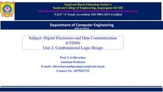
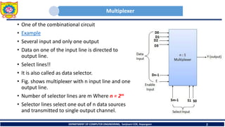
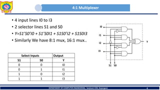
1. A multiplexer is a combinational circuit that selects one of several input lines and outputs the data on that line. It has multiple data inputs, a select line, and a single output. The value on the select line determines which input is directed to the output.
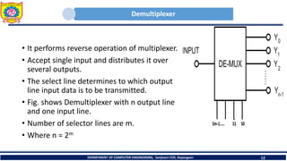
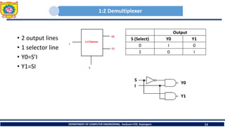
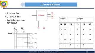
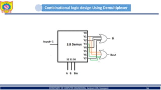
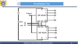
2. A demultiplexer is the reverse of a multiplexer. It has a single input and multiple outputs, with a select line determining which output the input data is directed to.
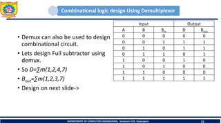
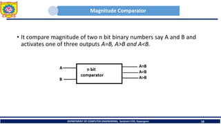
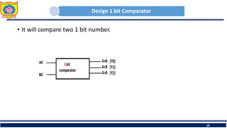
3. Combinational logic circuits like adders, comparators, and encoders can be designed using multiplexers and demultiplexers. Truth tables are used to derive the logic expressions implemented by the multiplexer/demultiplexer.