Downloaded 1,026 times
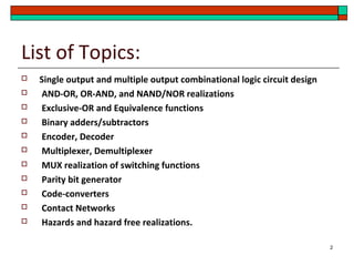
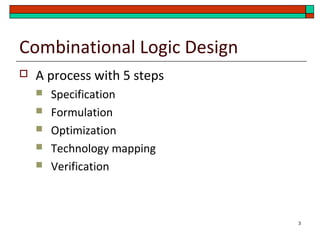
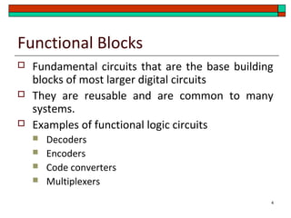
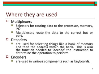
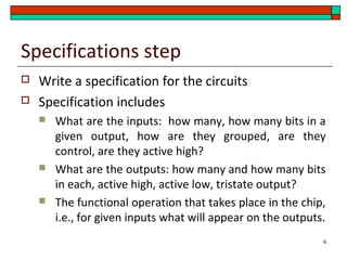
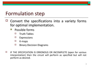
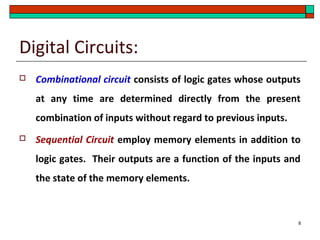
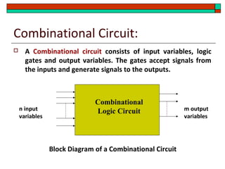
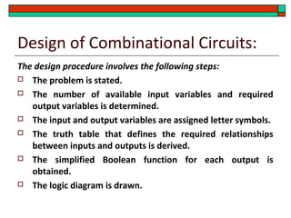
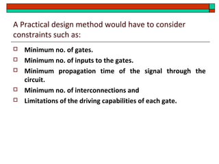
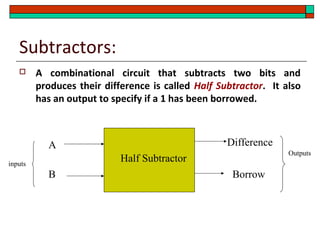
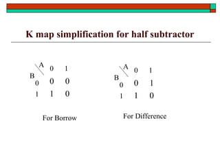
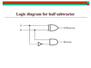
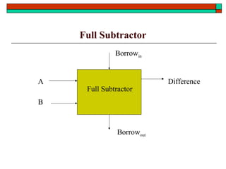
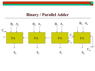
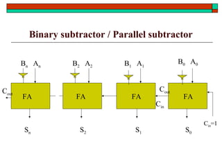
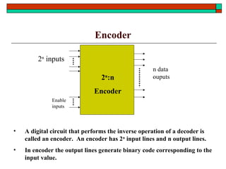
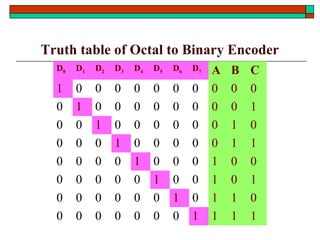
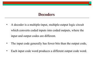
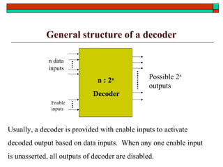
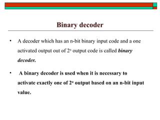
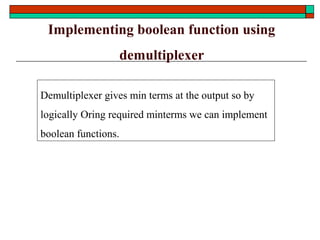
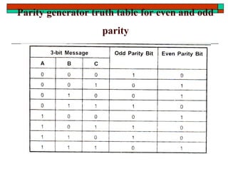
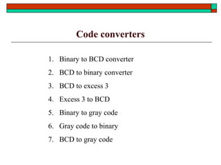
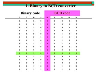
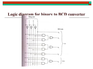
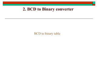
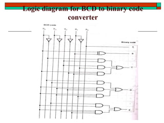


The document discusses various topics related to combinational logic design including: - The steps in the combinational logic design process including specification, formulation, optimization, technology mapping, and verification. - Common functional blocks like decoders, encoders, multiplexers and their uses. - Design of half adders, full adders, half subtractors, full subtractors and binary adders/subtractors. - Implementation of logic functions using multiplexers and demultiplexers. - Other topics like parity generators, code converters and hazards in combinational circuits.