Downloaded 176 times

![1
1
1
1
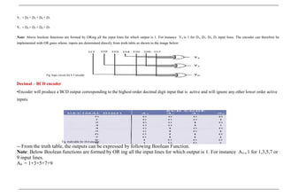
MODULE 3 MCA-102 DIGITAL SYSTEMS & LOGIC DESIGN ADMN 2014-‘17
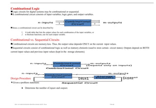
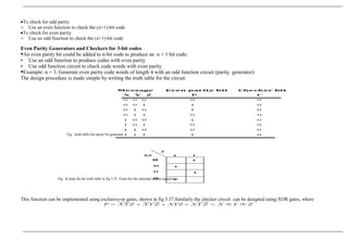
0 1
00
01
11
10
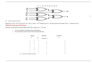
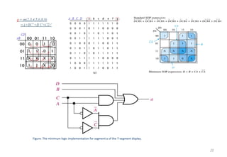
Fig : k-map for fig 3.39 From this the minimal output equation is
P=X’Y’Z’+X’YZ’+XYZ’+XY’Z
This function can be implemented using XOR and XNOR gates, shown in fig . Similarly the checker circuit can be designed using XOR and XNOR gates, where
X Y
Z
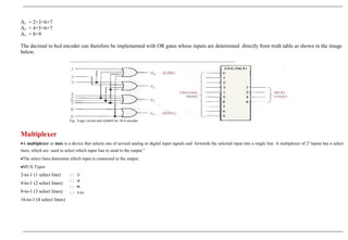
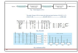
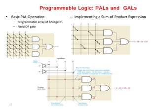
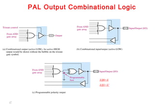
PLA [Programmable Logic Array]
Combination of a programmable AND array followed by a programmable OR array.
This layout allows for a large number of logic functions to be synthesized in the sum of products (and sometimes product of sums) canonical forms.](https://image.slidesharecdn.com/finaldigitallogicdesignpart2-170910143409/85/Digital-Logic-Design-25-320.jpg)
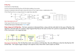
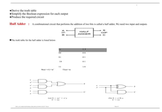
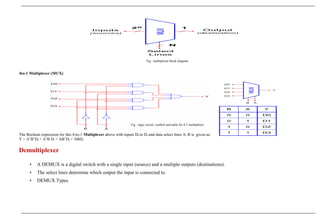
![Edge-triggered D flip-flop : The operations of a D flip-flop is much simpler. It has only one input addition to the clock. It is very
useful when a single data bit (0 or 1) is to be stored. If there is a HIGH on the D input when a clock pulse
is applied, the flip-flop SETs and stores a 1. If there is a LOW on the D input when a clock pulse is applied, the flip-flop RESETs and stores a 0. The truth table
below summarize the operations of the positive edge-triggered D flip-flop. As before, the negative edge-triggered flip-flop works the same except that the falling
edge of the clock pulse is the triggering edge.
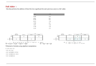
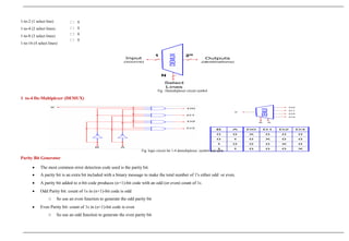
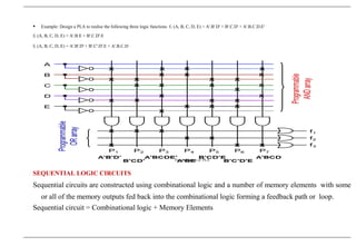
MASTER-SLAVE FLIP FLOP
Is designed using two separate flip flops. Out of these, one acts as the master and the other as a slave. The figure of a master-slave J-K flip flop is shown below.
Fig : master slave flip flop
From the above figure you can see that both the J-K flip flops are presented in a series connection. The output of the master J-K flip flop is fed to the
input of the slave J-K flip flop. The output of the slave J-K flip flop is given as a feedback to the input of the master J-K flip flop. The clock pulse
[Clk] is given to the master J-K flip flop and it is sent through a NOT Gate and thus inverted before passing it to the slave J-K flip flop.
When Clk=1, the master J-K flip flop gets disabled. The Clk input of the master input will be the
opposite of the slave input. So the master flip flop output will be recognized by the slave flip flop only when the Clk value becomes 0. Thus, when the
clock pulse males a transition from 1 to 0, the locked outputs of the master flip flop are fed through to the inputs of the slave flip-flop making this flip
flop edge or pulse-triggered.](https://image.slidesharecdn.com/finaldigitallogicdesignpart2-170910143409/85/Digital-Logic-Design-34-320.jpg)


This document provides information about Dr. Krishnanaik Vankdoth and his background and qualifications. It then discusses digital logic design topics like digital circuits, combinational logic, sequential circuits, logic gates, truth tables, adders, decoders, encoders, multiplexers and demultiplexers. Example circuits are provided and the functions of components like full adders, parallel adders, magnitude comparators are explained through diagrams and logic equations.