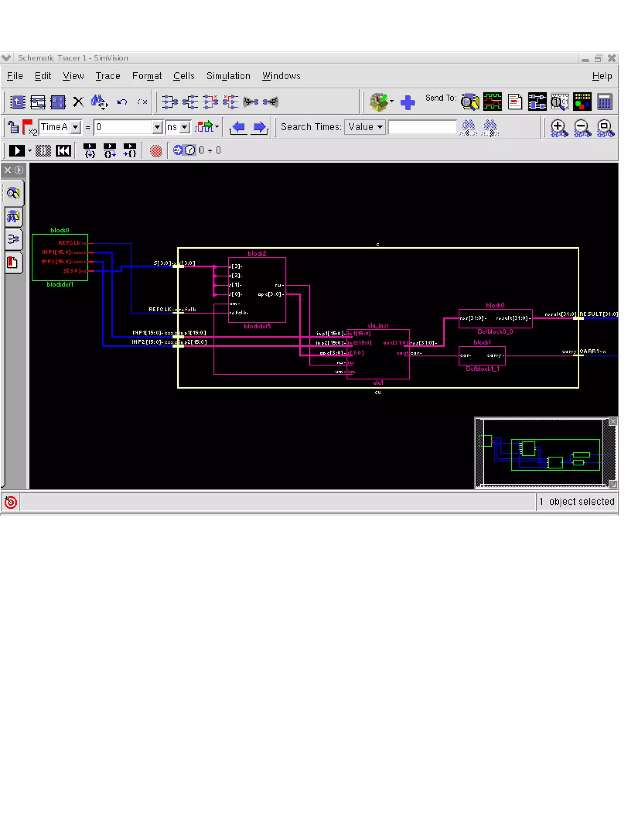
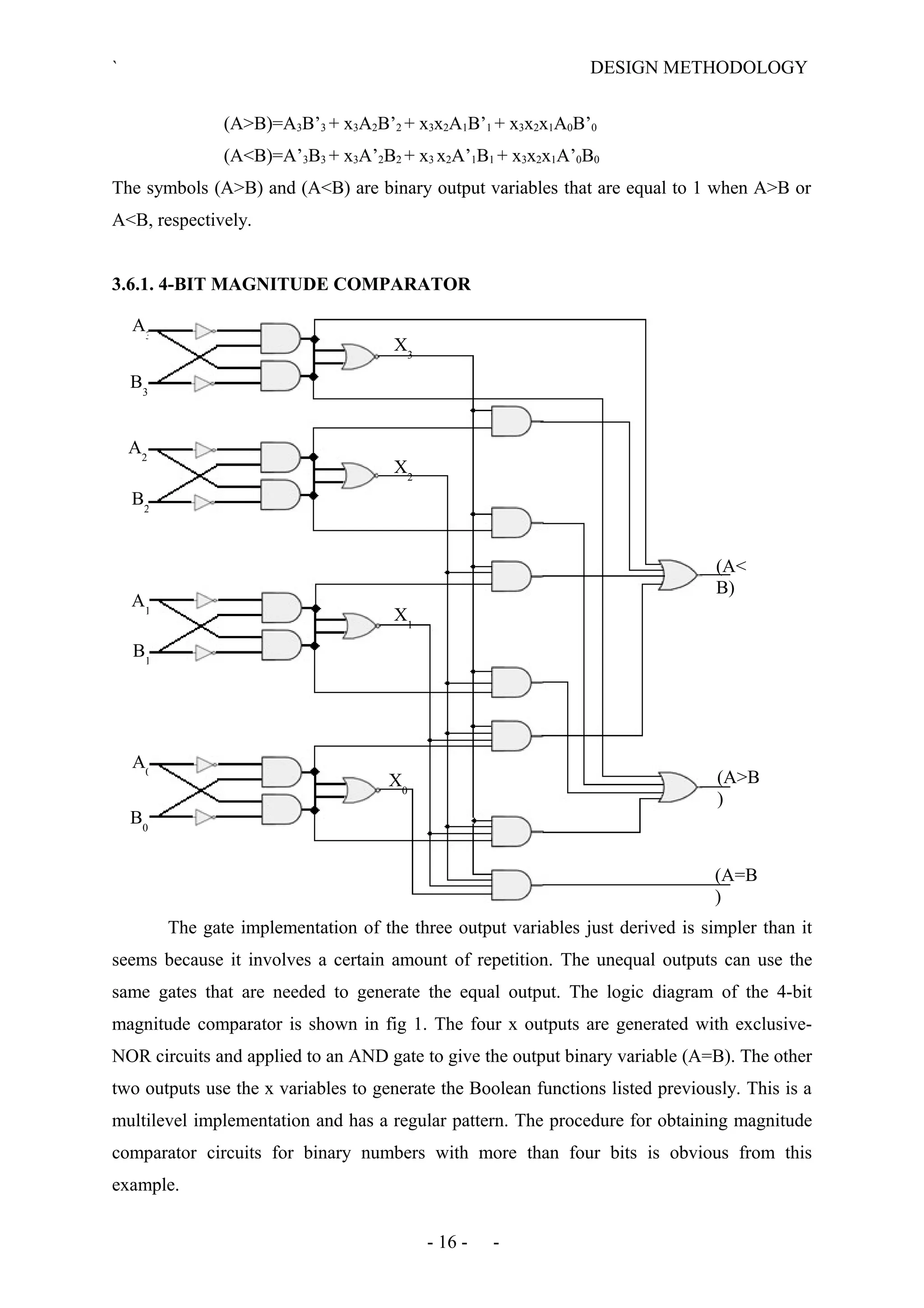
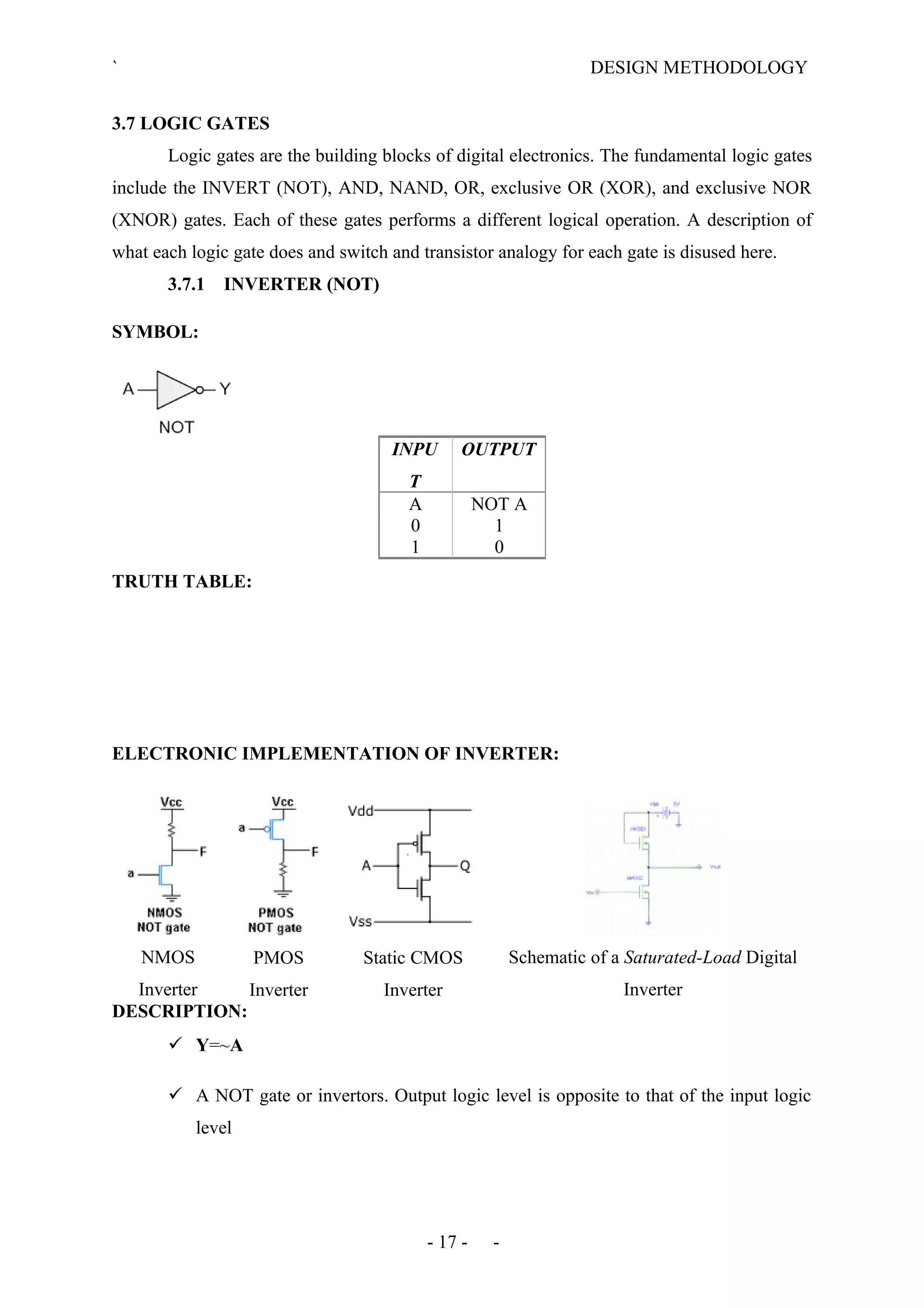
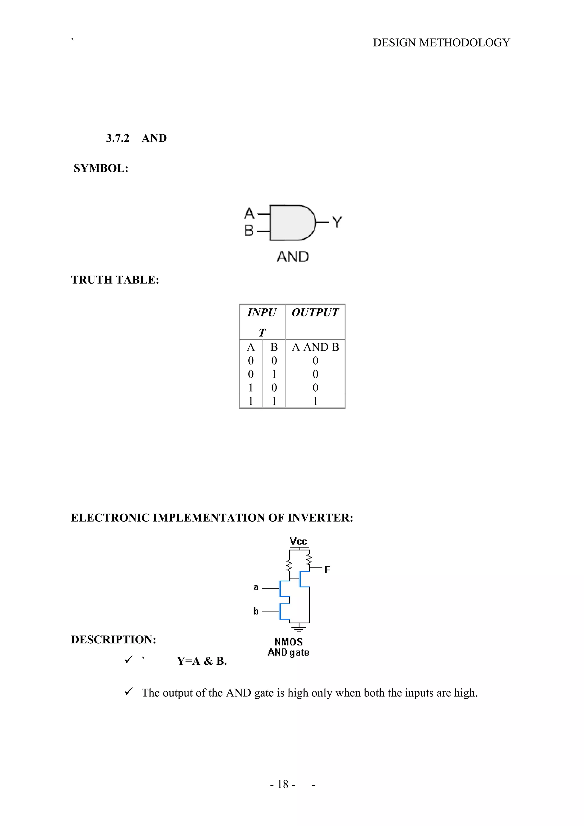
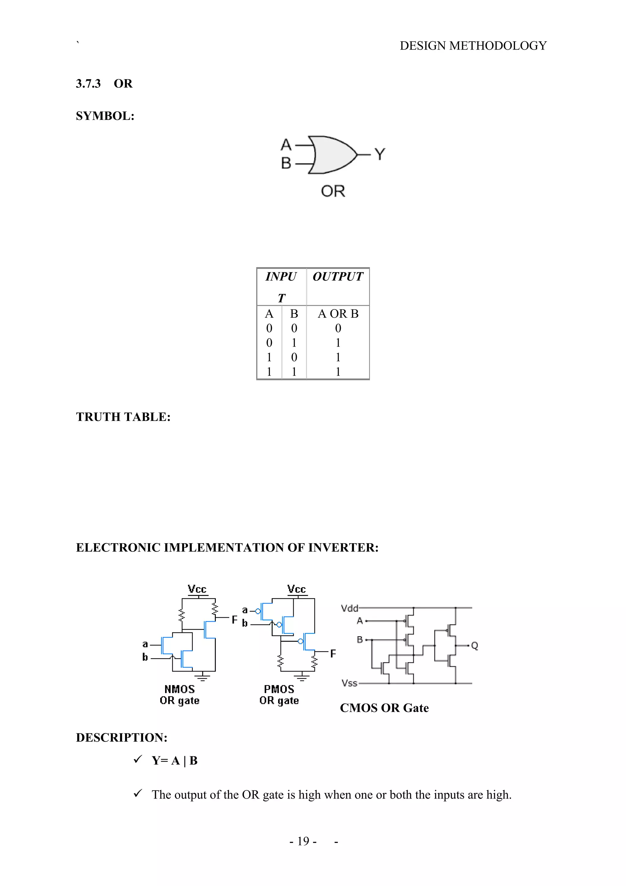
The document describes the design methodology for an ALU chip controller. It discusses using a carry look-ahead adder to speed up addition and subtraction. The ALU can perform various arithmetic (addition, subtraction, multiplication) and logical (AND, OR, XOR) operations. It uses a combinational logic design with multiplexers to select the output. The block diagram shows the main components are a control unit, 16-bit ALU, and memory. The control unit provides signals to control the ALU operations.
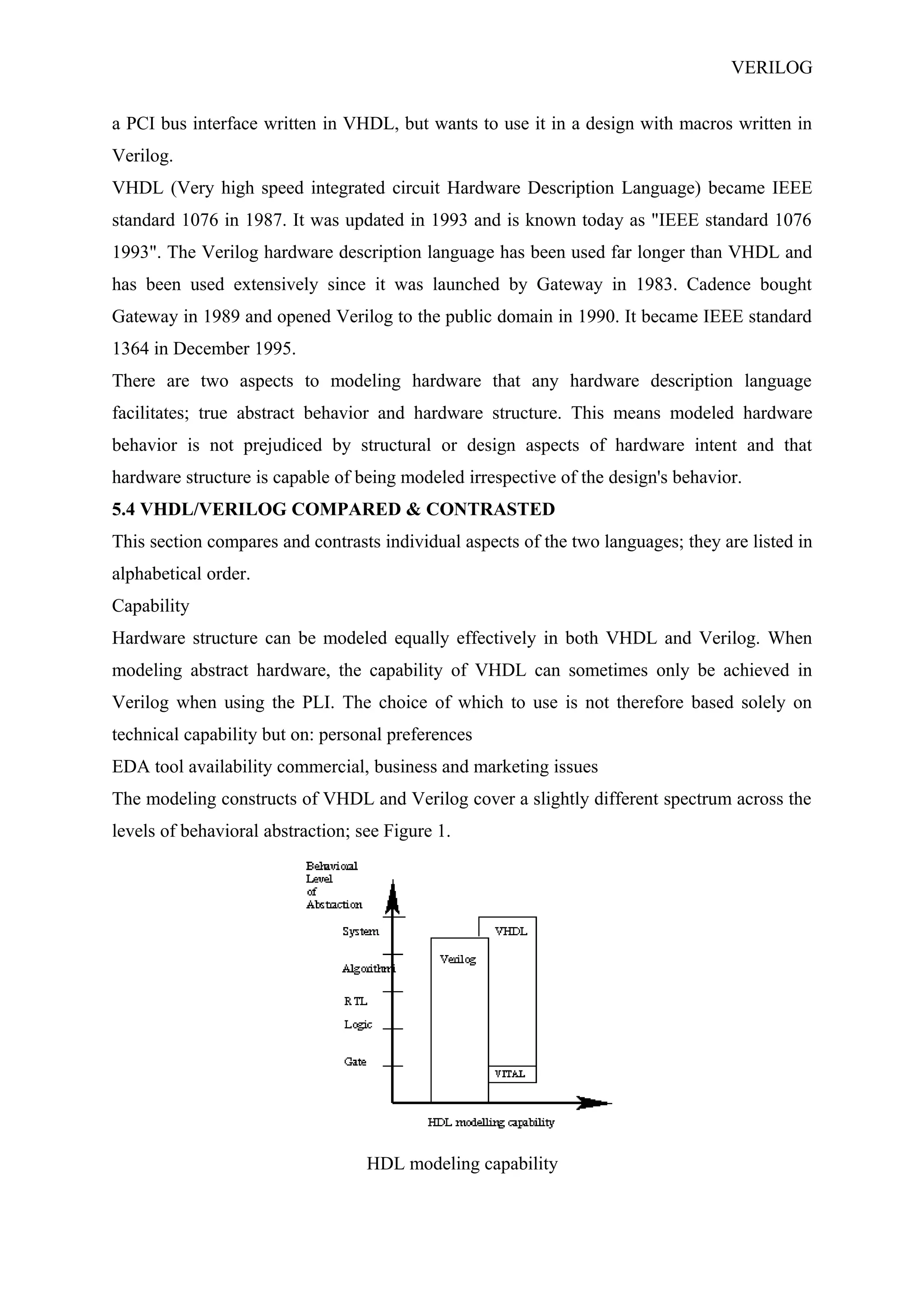
![BLOCK DIAGRAM AND ITS
FUNCTIONALITY
2.1 BLOCK DIAGRAM
The main blocks of the processor are
Control unit
ALU
Memory
CONTROL UNIT
It is the main block of the processor which controls the ALU. The 16 bit inputs, one 6 bit
selection line and clock input are given to this control unit. So that for every positive edge of
the clock the control unit must take the input and also output is given by control unit. The
control unit then tells the ALU what operation to be performed on the data with the help of
selection lines. It also tells the ALU whether to access memory or not.
ALU
As far as the ALU in our design is concerned, it loads data from two 16 bit data lines. The
ALU performs operations on that data according to the instructions given by the control unit.
- 4 - -
CONTROL
UNIT
16-BIT
ALU
MEMORY
16 X 65KBITS
[15:0]INPUT1
[15:0]INPUT2
[5:0]SELECT
CLOCK
[15:0]OUTPUT
CARRY
RW
[15:0]OUT
CARRY
[15:0]INPUT1
[15:0]INPUT2
[3:0]OPC
[15:0]ADDR
[15:0]DATAIN
[15:0]DATAOUT
RW
EN
EN](https://image.slidesharecdn.com/designofchipcontroller-140722122113-phpapp02/75/Design-of-chip-controller-4-2048.jpg)
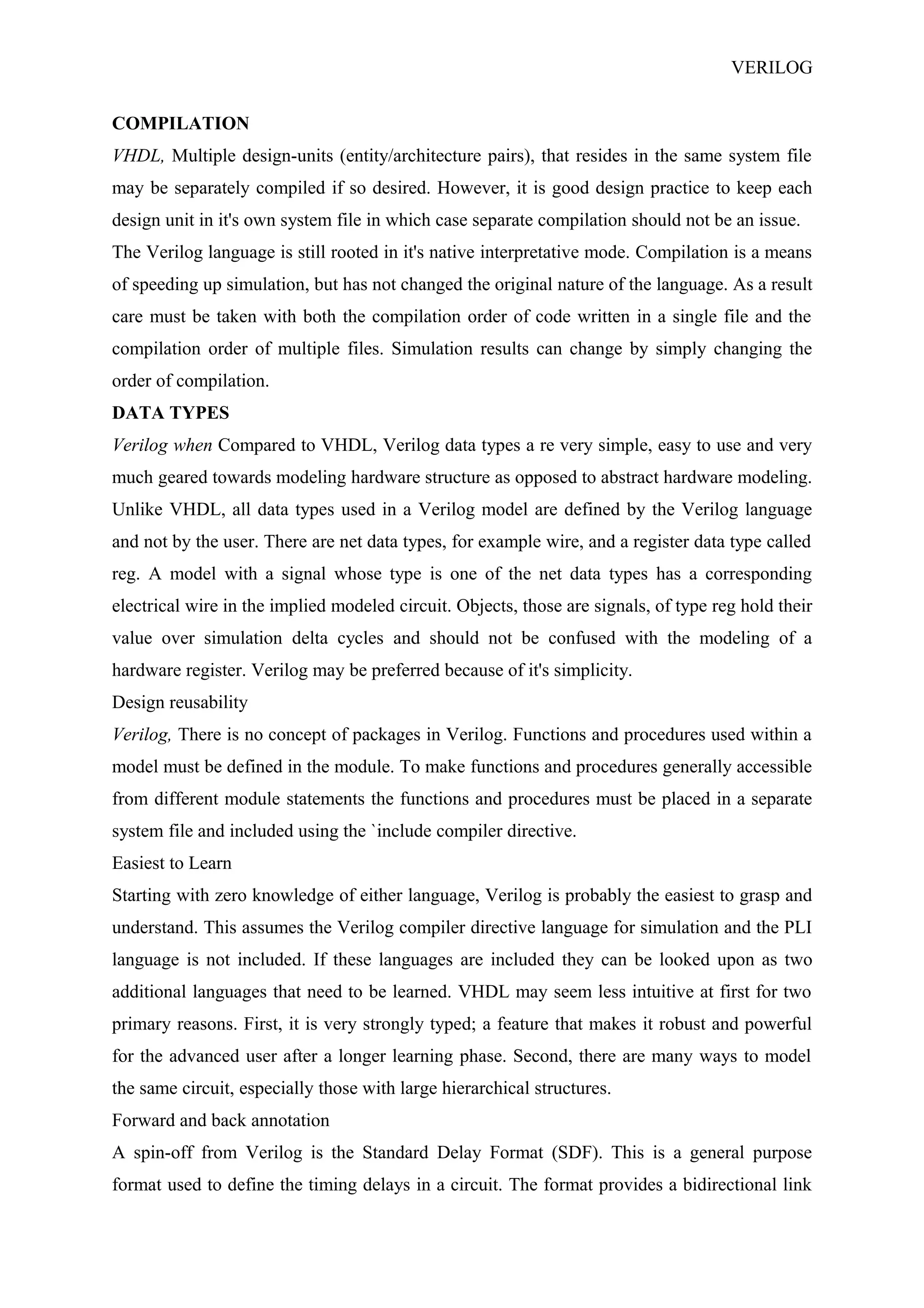
![2.2 OPCODES
S.N
O
OP-
CODE
SELECTION LINES FUNCTION MATHEMATICAL
REPRESENTAT-
ION
S[5] S[4] S[3] S[2] S[1] S[0]
1 32 1 0 0 0 0 0 Addition A + B
2 33 1 0 0 0 0 1 Subtraction A - B
3 34 1 0 0 0 1 0 Multiplication A * B
4 35 1 0 0 0 1 1 Or A | B
5 36 1 0 0 1 0 0 And A & B
6 37 1 0 0 1 0 1 Xor A ^ B
7 38 1 0 0 1 1 0 Not ~ A
8 39 1 0 0 1 1 1 Xnor A ~^ B
9 41 1 0 1 0 0 1 Comparison A>B,A<B,A=B
10 46 1 0 1 1 1 0 Buffer A
11 47 1 0 1 1 1 1 Buffer B
12 48 1 1 0 0 0 0 Addition A + MEM(B)
13 49 1 1 0 0 0 1 Subtraction A - MEM(B)
14 50 1 1 0 0 1 0 Multiplication A * MEM(B)
15 51 1 1 0 0 1 1 Or A | MEM(B)
16 52 1 1 0 1 0 0 And A & MEM(B)
17 53 1 1 0 1 0 1 Xor A ^ MEM(B)
18 54 1 1 0 1 1 0 Not ~ MEM(A)
19 55 1 1 0 1 1 1 Xnor A ~^ MEM(B)
20 57 1 1 1 0 0 1 Comparison A > MEM(B),
A < MEM(B),
A = MEM(B)
21 62 1 1 1 1 1 0 Buffer Move from memory
22 15 0 0 1 1 1 1 Buffer Move to memory
In selection lines each bit has its own significance. First four bits are used for selecting a
particular operation that has to perform on input data. Fifth bit tells the ALU
- 6 - -](https://image.slidesharecdn.com/designofchipcontroller-140722122113-phpapp02/75/Design-of-chip-controller-6-2048.jpg)
![`resetall
`timescale 1 ns / 1 ns
`view
module cu (inp1, inp2, s, refclk, result, carry);
input [15:0] inp1, inp2;
input [3:0] s;
input refclk;
output [31:0] result;
output carry;
reg [3:0] opc;
reg rw, um;
wire [31:0] res;
wire car, clk, spi_clk;
wire [15:0] data;
assign result = res;
assign carry = car;
alu1 alu_inst (inp1, inp2, opc, rw, um, res, car);
always @ (posedge refclk or rw or um or opc)
begin
opc = { s[3], s[2], s[1], s[0]};
if (um == 1)
begin
rw = 1;
end
else if (um == 0)
begin
rw = 1;
end
end
endmodule
`noview
MODULE – ALU
`resetall
`timescale 1 ns / 1 ns
`view
module alu (in1, in2, s, rw, um, out, cout);
input [15:0] in1,in2;
input [3:0] s;
input rw , um;
output [31:0] out;
output cout;
wire [31:0] out;
wire [15:0] out22, out33, out77;
wire [31:0] out88;
wire cout1;](https://image.slidesharecdn.com/designofchipcontroller-140722122113-phpapp02/75/Design-of-chip-controller-42-2048.jpg)
![wire [15:0] datout;
wire [1:0] ss;
reg [15:0] inn1, inn2, int, int1;
reg [15:0] out1,out3,out4,out5,out6,out7,out8,out9,out10;
reg [31:0] out2;
reg [15:0] m1,m2;
reg cc, en, e, enn;
assign
out = s[3] ? ( s[2] ? (s[1] ? (s[0] ? out10 : out9): out8 ): out8): ( s[2] ? ( s[1] ? ( s[0] ? out7:out6 ): ( s[0] : out5:
out4)): ( s[1] ? (s[0] ? out3 : out2) : out1));
assign cout = cout1;
add16 adder16bit_inst (in1, inn2, cc, enn, out22, cout1);
mul multiplication_inst (m1, m2, enn, out88);
cmpr comparator_inst (in1, int, e, ss, out77);
mem memory_inst (in2, in1, rw, en, datout);
always @ ( in1 or in2 or s or rw)
begin
en = 1;
if (um == 1);
int = datout;
else
int = in2;
inn2 <= {16{ s[0]}} ^ int;
cc <= s[0];
e <= 1;
m1 = { in1[15], in1[14], in1[13] , in1[12], in1[11], in1[10], in1[9], in1[8], in1[7], in1[6], in1[5], in1[4], in1[3],
in1[2], in1[1], in1[0]};
m2 = {int[15], int[14], int[13], int[12], int[11], int[10], int[9], int[8], int[7], int[6], int[5], int[4], int[3], int[2],
int[1], int[0]};
enn <= 1;
out6 = ~in1;
out2 = out88;
out3 = in1 | int;
out1 = out22;
out4 = in1 & int;
out5 = in1 ^ int;
out7 = out33;
out8 = out77;
out9 = in1;
out10 = int;
end
endmodule
`noview
MODULE – 16 BIT ADDER](https://image.slidesharecdn.com/designofchipcontroller-140722122113-phpapp02/75/Design-of-chip-controller-43-2048.jpg)
![`resetall
`timescale 1 ns / 1 ns
`view
module add16(a,b,c_in,Enn,sum,cout);
input [15:0] a,b;
input c_in;
input Enn;
output [15:0] sum;
output cout;
reg [15:0] p,g;
reg [16:0] carry;
reg [15:0]s;
integer i;
assign sum = s;
assign cout= carry[16];
always @ (Enn)
begin
p= (a ^ b);
g = (a & b);
carry[0] = c_in;
carry[1] = (g[0] | (p[0] & c_in));
carry[2] = (g[1] | (p[1] & g[0]) | (p[1] & p[0] & c_in));
carry[3] = (g[2] | (p[2] & g[1]) | (p[2] & p[1] & g[0]) | ( p[2] & p[1] & p[0] & c_in ));
carry[4] = (g[3] | (p[3] & g[2]) | (p[3] & p[2] & g[1]) | (p[3] & p[2] & p[1] & g[0]) | ( p[3] & p[2]
&
p[1] & p[0] & c_in));
carry[5] = (g[4] | (p[4] & g[3]) | (p[4] & p[3] & g[2]) | (p[4] & p[3] & p[2] & g[1]) | (p[4] & p[3]
& p[2] & p[1] & g[0]) | (p[4] & p[3] & p[2] & p[1] & p[0] & c_in));
carry[6] = (g[5] | (p[5] & g[4]) | (p[5] & p[4] & g[3]) | (p[5] & p[4] & p[3] & g[2]) | (p[5] & p[4]
& p[3] & p[2] & g[1]) | (p[5] & p[4] & p[3] & p[2] & p[1] & g[0]) | (p[5] & p[4] & p[3] & p[2]
& p[1] & p[0] & c_in));
carry[7] = (g[6] | (p[6] & g[5]) | (p[6] & p[5] & g[4]) | (p[6] & p[5] & p[4] & g[3]) | (p[6] & p[5]
& p[4] & p[3] & g[2]) | (p[6] & p[5] & p[4] & p[3] & p[2] & g[1]) | (p[6] & p[5] & p[4] & p[3]
& p[2] & p[1] & g[0]) | (p[6] & p[5] & p[4] & p[3] & p[2] & p[1] & p[0] & c_in));
carry[8] = (g[7] | (p[7] & g[6]) | (p[7] & p[6] & g[5]) | ( p[7] & p[6] & p[5] & g[4]) | ( p[7] & p[6]
& p[5] & p[4] & g[3]) | (p[7] & p[6] & p[5] & p[4] & p[3] & g[2]) | (p[7] & p[6] & p[5] & p[4]
& p[3] & p[2] & g[1]) | (p[7] & p[6] & p[5] & p[4] & p[3] & p[2] & p[1] & g[0]) | (p[7] & p[6]
& p[5] & p[4] & p[3] & p[2] & p[1] & p[0] & c_in));](https://image.slidesharecdn.com/designofchipcontroller-140722122113-phpapp02/75/Design-of-chip-controller-44-2048.jpg)
![carry[9] = (g[8] | (p[8] & g[7]) | ( p[8] & p[7] & g[6]) | (p[8] & p[7] & p[6] & g[5]) | (p[8] & p[7]
& p[6] & p[5] & g[4]) | (p[8] & p[7] & p[6] & p[5] & p[4] & g[3]) | (p[8] & p[7] & p[6] & p[5]
& p[4] & p[3] & g[2]) | (p[8] & p[7] & p[6] & p[5] & p[4] & p[3] & p[2] & g[1]) | (p[8] & p[7]
& p[6] & p[5] & p[4] & p[3] & p[2] & p[1] & g[0]) | (p[8] & p[7] & p[6] & p[5] & p[4] & p[3]
& p[2] & p[1] & p[0] & c_in));
carry[10] =( g[9] | (p[9] & g[8]) | ( p[9] & p[8] & g[7]) | (p[9] & p[8] & p[7] & g[6]) | (p[9] & p[8]
& p[7] & p[6] & g[5]) | (p[9] & p[8] & p[7] & p[6] & p[5] & g[4]) | (p[9] & p[8] & p[7] & p[6]
& p[5] & p[4] & g[3]) | (p[9] & p[8] & p[7] & p[6] & p[5] & p[4] & p[3] & g[2]) | (p[9] & p[8] &
p[7] & p[6] & p[5] & p[4] & p[4] & p[3] & p[2] & g[1]) | (p[9] & p[8] & p[7] & p[6] & p[5] &
p[4] & p[3] & p[2] & p[1] & g[0]) | (p[9] & p[8] & p[7] & p[6] & p[5] & p[4] & p[3] & p[2] &
p[1] & p[0] & c_in));
carry[11] = (g[10] | (p[10] & g[9]) | (p[10] & p[9] & g[8]) | (p[10] & p[9] & p[8] & g[7]) | ( p[10] &
p[9] & p[8] & p[7] & g[6]) | (p[10] & p[9] & p[8] & p[7] & p[6] & g[5]) | (p[10] & p[9] & p[8] &
p[7] & p[6] & p[5] & g[4]) | (p[10] & p[9] & p[8] & p[7] & p[6] & p[5] & p[4] & g[3]) | (p[10] &
p[9] & p[8] & p[7] & p[6] & p[5] & p[4] & p[3] & g[2]) | (p[10] & p[9] & p[8] & p[7] & p[6] &
p[5] & p[4] & p[3] & p[2] & g[1]) | (p[10] & p[9] & p[8] & p[7] & p[6] & p[5] & p[4] & p[3] &
p[2] & p[1] & g[0]) | (p[10] & p[9] & p[8] & p[7] & p[6] & p[5] & p[4] & p[3] & p[2] & p[1] &
p[0] & c_in));
carry[12] = (g[11] | (p[11] & g[10]) | (p[11] & p[10] & g[9]) | (p[11] & p[10] & p[9] & g[8]) |
( p[11] & p[10] & p[9] & p[8] & g[7]) | (p[11] & p[10] & p[9] & p[8] & p[7] & g[6]) | ( p[11] &
p[10] & p[9] & p[8] & p[7] & p[6] & g[5]) | (p[11] & p[10] & p[9] & p[8] & p[7] & p[6] & p[5]
& g[4]) | (p[11] & p[10] & p[9] & p[8] & p[7] & p[6] & p[5] & p[4] & g[3]) | ( p[11] & p[10] &
p[9] & p[8] & p[7] & p[6] & p[5] & p[4] & p[3] & g[2]) | (p[11] & p[10] & p[9] & p[8] & p[7]
& p[6] & p[5] & p[4] & p[3] & p[2] & g[1]) | (p[11] & p[10] & p[9] & p[8] & p[7] & p[6] & p[5]
& p[4] & p[3] & p[2] & p[1] & g[0]) | ( p[11] & p[10] & p[9] & p[8] & p[7] & p[6] & p[5] &
p[4] & p[3] & p[2] & p[1] & p[0] & c_in));
carry[13] = (g[12] | (p[12] & g[11]) | ( p[12] & p[11] & g[10] ) | (p[12] & p[11] & p[10] & g[9] ) |
( p[12] & p[11] & p[10] & p[9] & g[8]) | (p[12] & p[11] & p[10] & p[9] & p[8] & g[7] ) | (p[12]
& p[11] & p[10] & p[9] & p[8] & p[7] & g[6] ) | (p[12] & p[11] & p[10] & p[9] & p[8] & p[7] &
p[6] & g[5]) | (p[12] & p[11] & p[10] & p[9] & p[8] & p[7] & p[6] & p[5] & g[4]) | (p[12] &
p[11] & p[10] & p[9] & p[8] & p[7] & p[6] & p[5] & p[4] & g[3]) | (p[12] & p[11] & p[10] &
p[9] & p[8] & p[7] & p[6] & p[5] & p[4] & p[3] & g[2]) | (p[12] & p[11] & p[10] & p[9] & p[8] &
p[7] & p[6] & p[5] & p[4] & p[3] & p[2] & g[1]) | ( p[12] & p[11] & p[10] & p[9] & p[8] & p[7]
& p [6] & p[5] & p[4] & p[3] & p[2] & p[1] & g[0]) | (p[12] & p[11] & p[10] & p[9] & p[8] &
p[7] & p[6] & p[5] & p[4] & p[3] & p[2] & p[1] & p[0] & c_in));
carry[14] = (g[13] | (p[13] & g[12] ) | (p[13] & p[12] & g[11]) | (p[13] & p[12] & p[11] & g[10]) |
(p[13] & p[12] & p[11] & p[10] & g[9]) | (p[13] & p[12] & p[11] & p[10] & p[9] & g[8]) | (p[13]
& p[12] & p[11] & p[10] & p[9] & p[8] & g[7]) | (p[13] & p[12] & p[11] & p[10] & p[9] & p[8]
& p[7] & g[6]) | (p[13] & p[12] & p[11] & p[10] & p[9] & p[8] & p[7] & p[6] & g[5]) | (p[13] &
p[12] & p[11] & p[10] & p[9] & p[8] & p[7] & p[6] & p[5] & g[4]) | (p[13] & p[12] & p[11] &
p[10] & p[9] & p[8] & p[7] & p[6] & p[5] & p[4] & g[3]) | (p[13] & p[12] & p[11] & p[10] & p[9]
& p[8] & p[7] & p[6] & p[5] & p[4] & p[3] & g[2]) | (p[13] & p[12] & p[11] & p[10] & p[9] &
p[8] & p[7] & p[6] & p[5] & p[4] & p[3] & p[2] & g[1]) | (p[13] & p[12] & p[11] & p[10] & p[9]
& p[8] & p[7] & p[6] & p[5] & p[4] & p[3] & p[2] & p[1] & g[0]) | (p[13] & p[12] & p[11] &
p[10] & p[9] & p[8] & p[7] & p[6] & p[5] & p[4] & p[3] & p[2] & p[1] & p[0] & c_in));](https://image.slidesharecdn.com/designofchipcontroller-140722122113-phpapp02/75/Design-of-chip-controller-45-2048.jpg)
![carry[15] = (g[14] | (p[14] & g[13]) | (p[14] & p[13] & g[12] ) | (p[14] & p[13] & p[12] & g[11]) |
(p[14] & p[13] & p[12] & p[11] & g[10]) | ( p[14] & p[13] & p[12] & p[11] & p[10] & g[9] ) | ( p[14]
& p[13] & p[12] & p[11] & p[10] & p[9] & g[8]) | ( p[14] & p[13] & p[12] & p[11] & p[10] &
p[9] & p[8] & g[7]) | (p[14] & p[13] & p[12] & p[11] & p[10] & p[9] & p[8] & p[7] & g[6] ) |
( p[14] & p[13] & p[12] & p[11] & p[10] & p[9] & p[8] & p[7] & p[6] & g[5]) | (p[14] & p[13] &
p[12] & p[11] & p[10] & p[9] & p[8] & p[7] & p[6] & p[5] & g[4]) | (p[14] & p[13] & p[12] &
p[11] & p[10] & p[9] & p[8] & p[7] & p[ 6] & p[5] & p[4] & g[3]) | (p[14] & p[13] & p[12] &
p[11] & p[10] & p[9] & p[8] & p[7] & p[6] & p[5] & p[4] & p[3] & g[2]) | (p[14] & p[13] & p[12] &
p[11] & p[10] & p[9] & p[8] & p[7] & p[6] & p[5] & p[4] & p[3] & p[2] & g[1]) | (p[14] & p[13]
& p[12] & p[11] & p[10] & p[9] & p[8] & p[7] & p[6] & p[5] & p[4] & p [3] & p[2] & p[1] &
g[0]) | (p[14] & p[13] & p[12] & p[11] & p[10] & p[9] & p[8] & p[7] & p[6] & p[5] & p[4] &
p[3] & p[2] & p[1] & p[0] & c_in));
carry[16] = (g[15] | (p[15] & g[14]) | (p[15] & p[14] & g[13]) | (p[15] & p[14] & p[13] & g[12]) |
(p[15] & p[14] & p[13] & p[12] & g[11]) | (p[15] & p[14] & p[13] & p[12] & p[11] & g[10]) | (p[15]
& p[14] & p[13] & p[12] & p[11] & p[10] & g[9]) | ( p[15] & p[14] & p[13] & p[12] & p[11] &
p[10] & p[9] & g[8]) | (p[15] & p[14] & p[13] & p[12] & p[11] & p[10] & p[9] & p[8] & g[7]) | (p[15]
& p[14] & p[13] & p[12] & p[11] & p[10] & p[9] & p[8] & p[7] & g[6]) | (p[15] & p[14] & p[13]
& p[12] & p[11] & p[10] & p[9] & p[8] & p[7] & p[6] & g[5]) | (p[15] & p[14] & p[13] & p[12] &
p[11] & p[10] & p[9] & p[8] & p[7] & p[6] & p[5] & g[4]) | (p[15] & p[14] & p[13] & p[12] & p[11] &
p[10] & p[9] & p[8] & p[7] & p[6] & p[5] & p[4] & g[3]) | (p[15] & p[14] & p[13] & p[12] & p[11]
& p[10] & p[9] & p[8] & p[7] & p[6] & p[5] & p[4] & p[3] & g[2]) | (p[15] & p[14] & p[13] &
p[12] & p[11] & p[10] & p[9] & p[8] & p[7] & p[6] & p[5] & p[4] & p[3] & p[2] & g[1]) | ( p[15] &
p[14] & p[13] & p[12] & p[11] & p[10] & p[9] & p[8] & p[7] & p[6] & p[5] & p[4] & p[3] & p[2] &
p[1] & g[0]) | ( p[15] & p[14] & p[13] & p[12] & p[11] & p[10] & p[9] & p[8] & p[7] & p[6] & p[5]
& p[4] & p[3] & p[2] & p[1] & p[0] & c_in));
for( i =0 ;i< 16 ; i=i+1)
s[i] =(p[i] ^ carry[i]);
end
endmodule
MODULE – MULTIPLICATION
`resetall
`timescale 1 ns / 1 ns
`view
module mul(a,b,mult);
input [15:0] a,b;
output [31:0] mult;
integer i,j;
reg [15:0] prod1,prod,sum;
reg carry;
reg [31:0] m;
assign mult = m;
always @ (a or b)
begin
carry = 0;](https://image.slidesharecdn.com/designofchipcontroller-140722122113-phpapp02/75/Design-of-chip-controller-46-2048.jpg)
![for (j=0;j<16;j=j+1)
prod1[j]= a[0]& b[j];
m[0] = prod1[0];
prod1 = prod1 >> 1;
for (i=1;i<16;i=i+1)
begin
for (j = 0;j<16;j =j+1)
prod[j] = a[i] & b[j];
for(j=0;j<16;j=j+1)
begin
sum[j] = prod[j] ^ prod1[j] ^ carry;
carry = ( carry & prod[j]) | ( carry & prod1[j])| ( prod[j] & prod1[j]);
end
m[i]= sum [0];
prod1 = sum >> 1;
prod1[15] = carry;
end
for(i=0;i<16;i=i+1)
begin
m[i+16] = prod1[i];
end
end
endmodule
MODULE - COMPARATOR
`resetall
`timescale 1 ns/ 1 ns
`view
module cmpr(a,b,en,cmp,grt);
input [15:0] a,b;
input en;
output [1:0] cmp;
output [15:0] grt;
reg [15:0] x,ar,br,grtr;
integer i;
reg eq,gr,ls;
reg [15:0] c,d;
reg [1:0] compr;
assign cmp = compr;
assign grt = grtr;
always @ (en)
begin
ar = a;
br = b;
for ( i= 15; i > -1; i = i-1)
begin
x[i] = ( a[i] & b[i]) | (( ~a[i]) & (~b[i]));](https://image.slidesharecdn.com/designofchipcontroller-140722122113-phpapp02/75/Design-of-chip-controller-47-2048.jpg)
![c[i] = ~b[i];
d[i] = ~a[i];
end
eq = x[15] & x[14] & x[13] & x[12] & x[11] & x[10] & x[9] & x[8] & x[7] & x[6] & x[5] & x[4] & x[3] & x[2]
& x[1] & x[0];
gr = (a[15] & c[15]) | (x[15] & a[14] & c[14]) | (x[15] & x[14] & a[13] & c[13]) | (x[15] & x[14] & x[13] &
a[12] & c[12]) | ( x[15] & x[14] & x[13] & x[12] & a [11] & c [11]) | (x[15] & x[14] & x[13] & x[12] & x[11]
& a[10] & c[10]) | ( x[15] & x[14] & x[13] & x[12] & x[11] & x[10] & a[9] & c[9]) | (x[15] & x[14] & x[13] &
x[12] & x[11] & x[10] & x[9] & a[8] & c[8]) | (x[15] & x[14] & x[13] & x[12] & x[11] & x[10] & x[9] & x[8]
& a [7] & c[7]) | (x[15] & x[14] & x[13] & x[12] & x[11] & x[10] & x[9] & x[8] & x[7] & a[6] & c[6]) | (x[15]
& x[14] & x[13] & x[12] & x[11] & x[10] & x[9] & x[8] & x[7] & x[6] & a[5] & c[5]) | (x[15] & x[14] & x[13]
& x[12] & x[11] & x[10] & x[9] & x[8] & x[7] & x[6] & x[5] & a[4] & c[4]) | (x[15] & x[14] & x[13] & x[12]
& x[11] & x[10] & x[9] & x[8] & x[7] & x[6] & x[5] & x[4] & a[3] & c[3]) | (x[15] & x[14] & x[13] & x[12] &
x[11] & x[10] & x[9] & x[8] & x[7] & x[6] &x[5] & x[4] & x[3] & a[2] & c[2]) | (x[15] & x[14] & x[13] &
x[12] & x[11] & x[10] & x[9] & x[8] & x[7] & x[6] & x[5] & x[4] & x[3] & x[2] & a[1] & c[1]) | (x[15] &
x[14] & x[13] & x[12] & x[11] & x[10] & x[9] & x[8] & x[7] & x[6] & x[5] & x[4] & x[3] & x[2] &x[1] &
a[0] & c[0]);
ls = (d[15] & b[15]) | (x[15] & d[14] & b[14]) | (x[15] & x[14] & d[13] & b[13]) | (x[15] & x[14] & x[13] &
d[12] & b[12]) | ( x[15] & x[14] & x[13] & x[12] & d [11] & b [11]) | (x[15] & x[14] & x[13] & x[12] & x[11]
& d[10] & b[10]) | ( x[15] & x[14] & x[13] & x[12] & x[11] & x[10] & d[9] & b[9]) | (x[15] & x[14] & x[13] &
x[12] & x[11] & x[10] & x[9] & d[8] & b[8]) | (x[15] & x[14] &x[13] & x[12] & x[11] & x[10] & x[9] & x[8]
& d [7] & b[7]) | (x[15] & x[14] & x[13] & x[12] & x[11] & x[10] & x[9] & x[8] & x[7]& d[6] & b[6]) | (x[15]
& x[14] & x[13] & x[12] & x[11] & x[10] & x[9] & x[8] & x[7] & x[6] & d[5] & b[5]) | (x[15] & x[14] &
x[13] & x[12] & x[11] & x[10] & x[9] & x[8] & x[7] & x[6] & x[5] & d[4] & b[4]) | (x[15] & x[14] & x[13] &
x[12] & x[11] & x[10] & x[9] & x[8] & x[7] & x[6] & x[5] & x[4] & d[3] & b[3]) | (x[15] & x[14] & x[13] &
x[12] & x[11] & x[10] & x[9] & x[8] & x[7] & x[6] &x[5] & x[4] & x[3] & d[2] & b[2]) | (x[15] & x[14] &
x[13] & x[12] & x[11] & x[10] & x[9] & x[8] & x[7] & x[6] & x[5] & x[4] & x[3] & x[2] & d[1] & b[1]) |
(x[15] & x[14] & x[13] & x[12] & x[11] & x[10] & x[9] & x[8] & x[7] & x[6] & x[5] & x[4] & x[3] & x[2]
&x[1] & d[0] & b[0]);
if (eq == 1)
begin
compr = 2'b00;
grtr = ar;
end
else if (gr == 1)
begin
compr = 2'b01;
grtr = ar;
end
else if ( ls == 1)
begin
compr = 2'b10;
grtr = br;
end
else
compr = 2'b11;
end
endmodule](https://image.slidesharecdn.com/designofchipcontroller-140722122113-phpapp02/75/Design-of-chip-controller-48-2048.jpg)
![MODULE – MEMORY
`resetall
`timescale 1 ns/ 1 ns
`view
module mem(addr,datain,rw,en,dataout);
input [15:0] datain,addr;
output [15:0] dataout;
input rw,en;
reg [65535:0] mem1 [15:0];
reg [15:0] dat;
assign dataout = dat;
always @ (en)
begin
if(rw==1)
dat = mem1[addr];
else if(rw==0)
begin
mem1[addr] = datain;
dat = datain;
end
dat= datain;
end
endmodule
`noview](https://image.slidesharecdn.com/designofchipcontroller-140722122113-phpapp02/75/Design-of-chip-controller-49-2048.jpg)