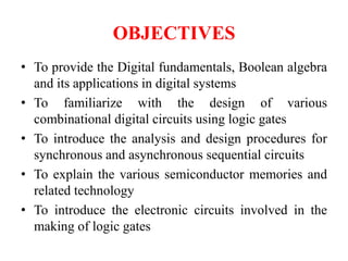
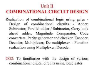
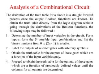
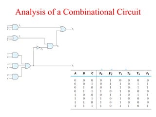
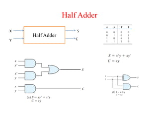
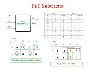
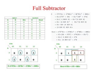
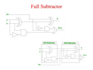
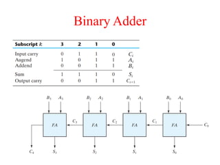
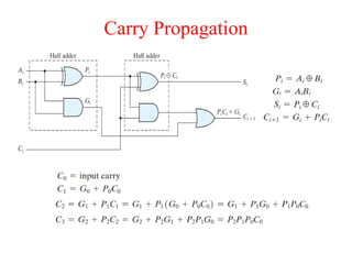
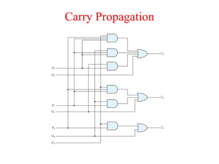
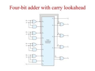
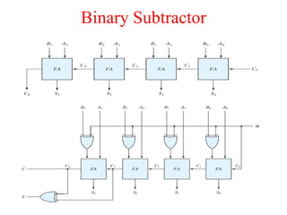
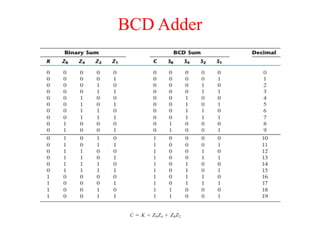
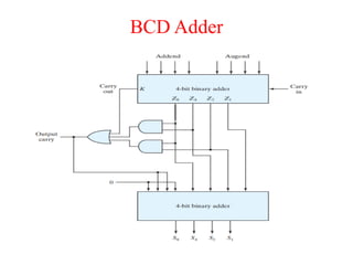
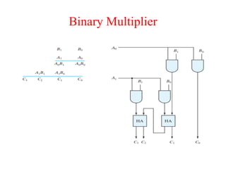
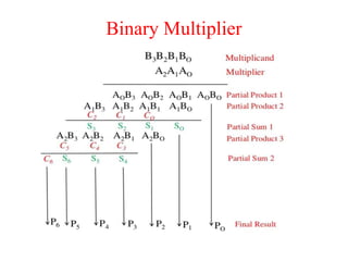
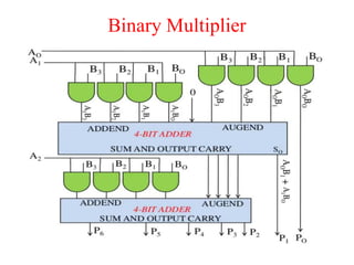
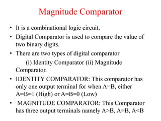
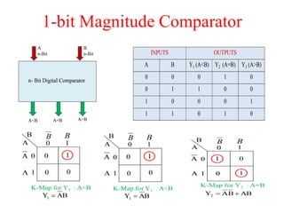
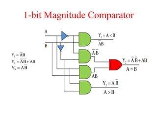
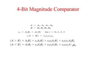
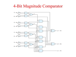
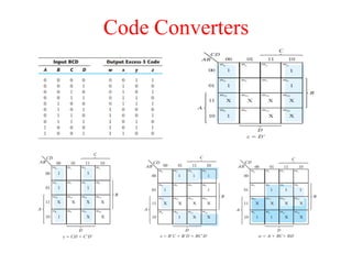
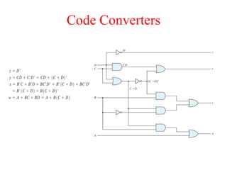
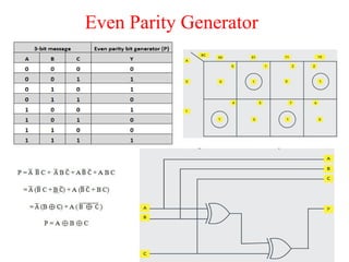
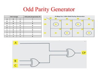
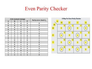
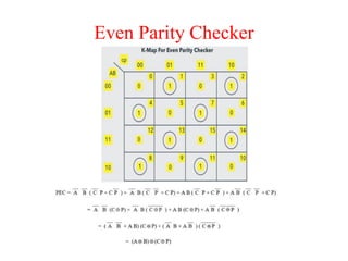
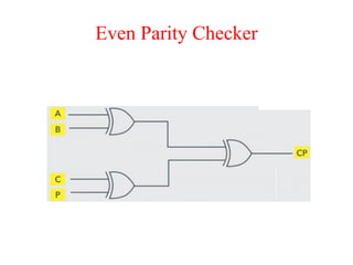
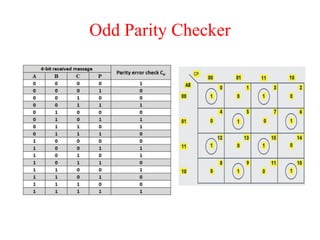
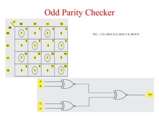
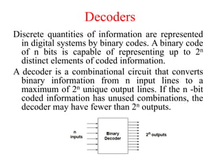
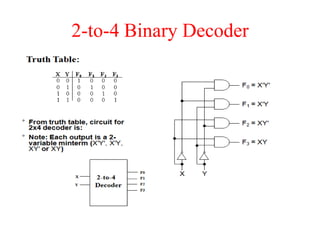
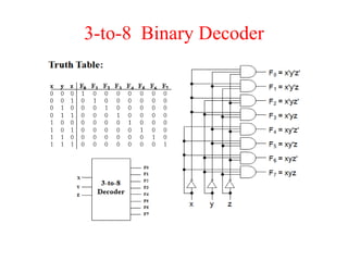
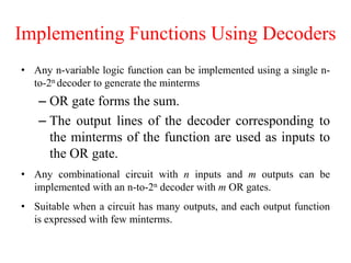
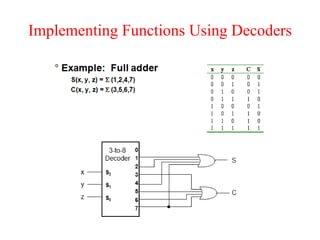
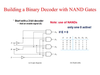
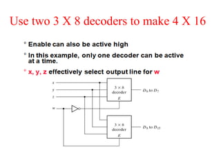
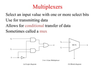
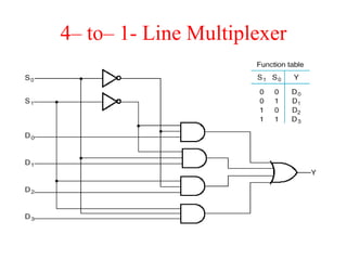
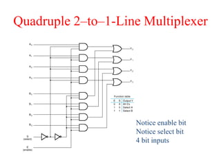
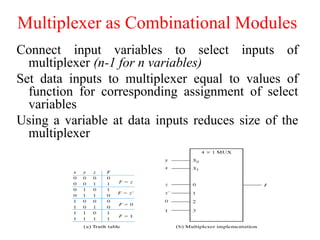
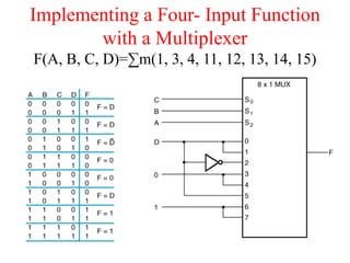
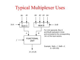
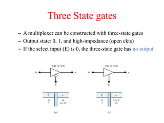
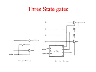
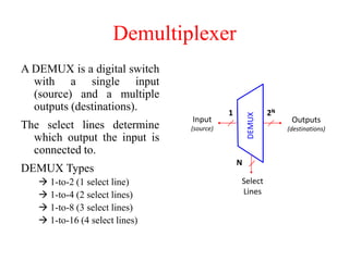
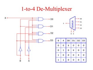
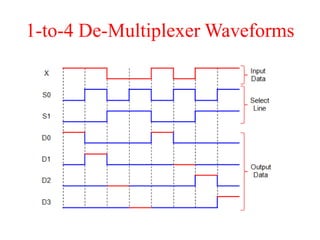
EC1371 – DIGITAL ELECTRONICS
Dr. K. Kannan, M.E., M.E., Ph.D.,
Professor & Head,
Department of Mechatronics Engineering
OBJECTIVES
• To provide the Digital fundamentals, Boolean algebra
and its applications in digital systems
• To familiarize with the design of various
combinational digital circuits using logic gates
• To introduce the analysis and design procedures for
synchronous and asynchronous sequential circuits
• To explain the various semiconductor memories and
related technology
• To introduce the electronic circuits involved in the
making of logic gates
Unit II
COMBINATIONAL CIRCUIT DESIGN
Realization of combinational logic using gates -
Design of combinational circuits - Adder,
Subtractor, Parallel adder / Subtractor, Carry look
ahead adder, Magnitude Comparator, Code
converters, Parity generator and checker, Encoder,
Decoder, Multiplexer, De-multiplexer - Function
realization using Multiplexer, Decoder.
CO2: To familiarize with the design of various
combinational digital circuits using logic gates
COMBINATIONAL CIRCUIT
Logic circuits may be combinational or
sequential.
A combinational circuit consists of logic gates
whose outputs at any time are determined from
only the present combination of inputs.
Analysis of a Combinational Circuit
The analysis of a combinational circuit starts with a given logic
diagram and culminates with a set of Boolean functions, a
truth table, and / or an explanation of the circuit operation.
Steps are:
1. Label all gate outputs that are a function of input variables
with arbitrary symbols. Determine the Boolean functions for
each gate output.
2. Label the gates that are a function of input variables and
previously labeled gates with other arbitrary symbols. Find
the Boolean functions for these gates.
3. Repeat the process outlined in step 2 until the outputs of the
circuit are obtained.
4. By repeated substitution of previously defined functions,
obtain the output Boolean functions in terms of input
variables.
Analysis of a Combinational Circuit
The derivation of the truth table for a circuit is a straight forward
process once the output Boolean functions are known. To
obtain the truth table directly from the logic diagram without
going through the derivations of the Boolean functions, the
following steps may be followed :
1. Determine the number of input variables in the circuit. For n
inputs, form the 2n possible input combinations and list the
binary numbers from 0 to (2n - 1) in a table.
2. Label the outputs of selected gates with arbitrary symbols.
3. Obtain the truth table for the outputs of those gates which are
a function of the input variables only.
4. Proceed to obtain the truth table for the outputs of those gates
which are a function of previously defined values until the
columns for all outputs are determined.
Analysis of a Combinational Circuit
The design of combinational circuits starts from the specification of the
design objective and culminates in a logic circuit diagram or a set of
Boolean functions from which the logic diagram can be obtained.
The procedure involves the following steps:
1. From the specifications of the circuit, determine the required
number of inputs and outputs and assign a symbol to each.
2. Derive the truth table that defines the required relationship between
inputs and outputs.
3. Obtain the simplified Boolean functions for each output as a
function of the input variables.
4. Draw the logic diagram and verify the correctness of the design
(manually or by simulation).
Design of a Combinational Circuit
Half Adder
Half Adder
X
Y
S
C
Half Subtractor
Full Adder
Full Adder
Full Adder
Full Subtractor
Full Subtractor
Full Subtractor
Binary Adder
Carry Propagation
Carry Propagation
Four-bit adder with carry lookahead
Binary Subtractor
BCD Adder
BCD Adder
Binary Multiplier
Binary Multiplier
Binary Multiplier
Magnitude Comparator
• It is a combinational logic circuit.
• Digital Comparator is used to compare the value of
two binary digits.
• There are two types of digital comparator
(i) Identity Comparator (ii) Magnitude
Comparator.
• IDENTITY COMPARATOR: This comparator has
only one output terminal for when A=B, either
A=B=1 (High) or A=B=0 (Low)
• MAGNITUDE COMPARATOR: This Comparator
has three output terminals namely A>B, A=B, A<B
1-bit Magnitude Comparator
2-Bit Magnitude Comparator
4-Bit Magnitude Comparator
Code Converters
Code Converters
Parity Generator
It is combinational circuit that accepts an n-1 bit data and
generates the additional bit that is to be transmitted
with the bit stream. This additional or extra bit is called
as a Parity Bit.
In even parity bit scheme, the parity bit is ‘0’ if there are
even number of 1s in the data stream and the parity bit
is ‘1’ if there are odd number of 1s in the data stream.
In odd parity bit scheme, the parity bit is ‘1’ if there are
even number of 1s in the data stream and the parity bit
is ‘0’ if there are odd number of 1s in the data stream.
Let us discuss both even and odd parity generators.
Even Parity Generator
Odd Parity Generator
Parity Check
It is a logic circuit that checks for possible errors
in the transmission. This circuit can be an even
parity checker or odd parity checker depending
on the type of parity generated at the
transmission end. When this circuit is used as
even parity checker, the number of input bits
must always be even.
Even Parity Checker
Even Parity Checker
Even Parity Checker
Odd Parity Checker
Odd Parity Checker
Decoders
Discrete quantities of information are represented
in digital systems by binary codes. A binary code
of n bits is capable of representing up to 2n
distinct elements of coded information.
A decoder is a combinational circuit that converts
binary information from n input lines to a
maximum of 2n unique output lines. If the n -bit
coded information has unused combinations, the
decoder may have fewer than 2n outputs.
2-to-4 Binary Decoder
3-to-8 Binary Decoder
Implementing Functions Using Decoders
• Any n-variable logic function can be implemented using a single n-
to-2n decoder to generate the minterms
– OR gate forms the sum.
– The output lines of the decoder corresponding to
the minterms of the function are used as inputs to
the OR gate.
• Any combinational circuit with n inputs and m outputs can be
implemented with an n-to-2n decoder with m OR gates.
• Suitable when a circuit has many outputs, and each output function
is expressed with few minterms.
Implementing Functions Using Decoders
Building a Binary Decoder with NAND Gates
Use two 3 X 8 decoders to make 4 X 16
Encoders
8-to-3 Binary Encoder
8-to-3 Priority Encoder
Multiplexers
Select an input value with one or more select bits
Use for transmitting data
Allows for conditional transfer of data
Sometimes called a mux
4– to– 1- Line Multiplexer
Quadruple 2–to–1-Line Multiplexer
Notice enable bit
Notice select bit
4 bit inputs
Multiplexer as Combinational Modules
Connect input variables to select inputs of
multiplexer (n-1 for n variables)
Set data inputs to multiplexer equal to values of
function for corresponding assignment of select
variables
Using a variable at data inputs reduces size of the
multiplexer
Implementing a Four- Input Function
with a Multiplexer
F(A, B, C, D)=∑m(1, 3, 4, 11, 12, 13, 14, 15)
Typical Multiplexer Uses
Three State gates
– A multiplexer can be constructed with three-state gates
– Output state: 0, 1, and high-impedance (open ckts)
– If the select input (E) is 0, the three-state gate has no output
Three State gates
Demultiplexer
A DEMUX is a digital switch
with a single input
(source) and a multiple
outputs (destinations).
The select lines determine
which output the input is
connected to.
DEMUX Types
 1-to-2 (1 select line)
 1-to-4 (2 select lines)
 1-to-8 (3 select lines)
 1-to-16 (4 select lines)
Select
Lines
Input
(source)
Outputs
(destinations)
2N
1
N
DEMUX
1-to-4 De-Multiplexer
D0
D1
D2
D3
X
B A
DEMUX
B A D0 D1 D2 D3
0 0 X 0 0 0
0 1 0 X 0 0
1 0 0 0 X 0
1 1 0 0 0 X
1-to-4 De-Multiplexer Waveforms
Thank You

Digital Electronics-Unit II.pdf

  • 1.
    EC1371 – DIGITALELECTRONICS Dr. K. Kannan, M.E., M.E., Ph.D., Professor & Head, Department of Mechatronics Engineering
  • 2.
    OBJECTIVES • To providethe Digital fundamentals, Boolean algebra and its applications in digital systems • To familiarize with the design of various combinational digital circuits using logic gates • To introduce the analysis and design procedures for synchronous and asynchronous sequential circuits • To explain the various semiconductor memories and related technology • To introduce the electronic circuits involved in the making of logic gates
  • 3.
    Unit II COMBINATIONAL CIRCUITDESIGN Realization of combinational logic using gates - Design of combinational circuits - Adder, Subtractor, Parallel adder / Subtractor, Carry look ahead adder, Magnitude Comparator, Code converters, Parity generator and checker, Encoder, Decoder, Multiplexer, De-multiplexer - Function realization using Multiplexer, Decoder. CO2: To familiarize with the design of various combinational digital circuits using logic gates
  • 4.
    COMBINATIONAL CIRCUIT Logic circuitsmay be combinational or sequential. A combinational circuit consists of logic gates whose outputs at any time are determined from only the present combination of inputs.
  • 5.
    Analysis of aCombinational Circuit The analysis of a combinational circuit starts with a given logic diagram and culminates with a set of Boolean functions, a truth table, and / or an explanation of the circuit operation. Steps are: 1. Label all gate outputs that are a function of input variables with arbitrary symbols. Determine the Boolean functions for each gate output. 2. Label the gates that are a function of input variables and previously labeled gates with other arbitrary symbols. Find the Boolean functions for these gates. 3. Repeat the process outlined in step 2 until the outputs of the circuit are obtained. 4. By repeated substitution of previously defined functions, obtain the output Boolean functions in terms of input variables.
  • 6.
    Analysis of aCombinational Circuit
  • 7.
    Analysis of aCombinational Circuit
  • 8.
    The derivation ofthe truth table for a circuit is a straight forward process once the output Boolean functions are known. To obtain the truth table directly from the logic diagram without going through the derivations of the Boolean functions, the following steps may be followed : 1. Determine the number of input variables in the circuit. For n inputs, form the 2n possible input combinations and list the binary numbers from 0 to (2n - 1) in a table. 2. Label the outputs of selected gates with arbitrary symbols. 3. Obtain the truth table for the outputs of those gates which are a function of the input variables only. 4. Proceed to obtain the truth table for the outputs of those gates which are a function of previously defined values until the columns for all outputs are determined. Analysis of a Combinational Circuit
  • 9.
    Analysis of aCombinational Circuit
  • 10.
    The design ofcombinational circuits starts from the specification of the design objective and culminates in a logic circuit diagram or a set of Boolean functions from which the logic diagram can be obtained. The procedure involves the following steps: 1. From the specifications of the circuit, determine the required number of inputs and outputs and assign a symbol to each. 2. Derive the truth table that defines the required relationship between inputs and outputs. 3. Obtain the simplified Boolean functions for each output as a function of the input variables. 4. Draw the logic diagram and verify the correctness of the design (manually or by simulation). Design of a Combinational Circuit
  • 11.
  • 12.
  • 13.
  • 14.
  • 15.
  • 16.
  • 17.
  • 18.
  • 19.
  • 20.
  • 21.
  • 22.
    Four-bit adder withcarry lookahead
  • 23.
  • 24.
  • 25.
  • 26.
  • 27.
  • 28.
  • 29.
    Magnitude Comparator • Itis a combinational logic circuit. • Digital Comparator is used to compare the value of two binary digits. • There are two types of digital comparator (i) Identity Comparator (ii) Magnitude Comparator. • IDENTITY COMPARATOR: This comparator has only one output terminal for when A=B, either A=B=1 (High) or A=B=0 (Low) • MAGNITUDE COMPARATOR: This Comparator has three output terminals namely A>B, A=B, A<B
  • 30.
  • 31.
  • 32.
  • 33.
  • 34.
  • 35.
  • 36.
  • 37.
  • 38.
  • 39.
  • 40.
    Parity Generator It iscombinational circuit that accepts an n-1 bit data and generates the additional bit that is to be transmitted with the bit stream. This additional or extra bit is called as a Parity Bit. In even parity bit scheme, the parity bit is ‘0’ if there are even number of 1s in the data stream and the parity bit is ‘1’ if there are odd number of 1s in the data stream. In odd parity bit scheme, the parity bit is ‘1’ if there are even number of 1s in the data stream and the parity bit is ‘0’ if there are odd number of 1s in the data stream. Let us discuss both even and odd parity generators.
  • 41.
  • 42.
  • 43.
    Parity Check It isa logic circuit that checks for possible errors in the transmission. This circuit can be an even parity checker or odd parity checker depending on the type of parity generated at the transmission end. When this circuit is used as even parity checker, the number of input bits must always be even.
  • 44.
  • 45.
  • 46.
  • 47.
  • 48.
  • 49.
    Decoders Discrete quantities ofinformation are represented in digital systems by binary codes. A binary code of n bits is capable of representing up to 2n distinct elements of coded information. A decoder is a combinational circuit that converts binary information from n input lines to a maximum of 2n unique output lines. If the n -bit coded information has unused combinations, the decoder may have fewer than 2n outputs.
  • 50.
  • 51.
  • 52.
    Implementing Functions UsingDecoders • Any n-variable logic function can be implemented using a single n- to-2n decoder to generate the minterms – OR gate forms the sum. – The output lines of the decoder corresponding to the minterms of the function are used as inputs to the OR gate. • Any combinational circuit with n inputs and m outputs can be implemented with an n-to-2n decoder with m OR gates. • Suitable when a circuit has many outputs, and each output function is expressed with few minterms.
  • 53.
  • 54.
    Building a BinaryDecoder with NAND Gates
  • 55.
    Use two 3X 8 decoders to make 4 X 16
  • 56.
  • 57.
  • 58.
  • 59.
  • 60.
    Multiplexers Select an inputvalue with one or more select bits Use for transmitting data Allows for conditional transfer of data Sometimes called a mux
  • 61.
    4– to– 1-Line Multiplexer
  • 62.
    Quadruple 2–to–1-Line Multiplexer Noticeenable bit Notice select bit 4 bit inputs
  • 63.
    Multiplexer as CombinationalModules Connect input variables to select inputs of multiplexer (n-1 for n variables) Set data inputs to multiplexer equal to values of function for corresponding assignment of select variables Using a variable at data inputs reduces size of the multiplexer
  • 64.
    Implementing a Four-Input Function with a Multiplexer F(A, B, C, D)=∑m(1, 3, 4, 11, 12, 13, 14, 15)
  • 65.
  • 66.
    Three State gates –A multiplexer can be constructed with three-state gates – Output state: 0, 1, and high-impedance (open ckts) – If the select input (E) is 0, the three-state gate has no output
  • 67.
  • 68.
    Demultiplexer A DEMUX isa digital switch with a single input (source) and a multiple outputs (destinations). The select lines determine which output the input is connected to. DEMUX Types  1-to-2 (1 select line)  1-to-4 (2 select lines)  1-to-8 (3 select lines)  1-to-16 (4 select lines) Select Lines Input (source) Outputs (destinations) 2N 1 N DEMUX
  • 69.
    1-to-4 De-Multiplexer D0 D1 D2 D3 X B A DEMUX BA D0 D1 D2 D3 0 0 X 0 0 0 0 1 0 X 0 0 1 0 0 0 X 0 1 1 0 0 0 X
  • 70.
  • 71.