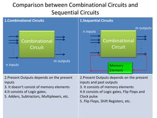
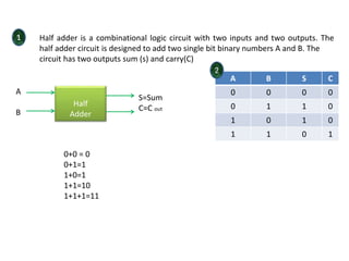
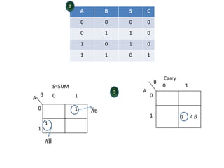
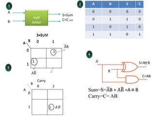
Combinational Logic Circuits
T.V.Hyma Lakshmi
Contents
1. Introduction
2. Designing Steps
3. Example :Half Adder
Digital circuits are divided into
two types:
1. Combinational Logic Circuits
2. Sequential Logic Circuits
1.Combinational Circuits 1.Sequential Circuits
2.Present Outputs depends on the present
inputs
3. It doesn’t consist of memory elements
4.It consists of Logic gates.
5. Adders, Subtractors, Multiplexers, etc.
2.Present Outputs depends on the present
inputs and past outputs
3. It consists of memory elements
4.It consists of Logic gates, Flip Flops and
Clock pulse
5. Flip Flops, Shift Registers, etc.
Comparison between Combinational Circuits and
Sequential Circuits
Combinational
Circuit
n inputs
m outputs
Combinational
Circuit
n inputs
m outputs
Memory
Element
Designing Steps: The design procedure for
combinational logic circuits starts with the problem
statement, ends at logic circuits diagram and comprises
the following steps:
1.Determine required number of inputs and outputs from the
specifications.
2.Derive the truth table for each of the outputs based on their
relationships to the input.
3.Simplify the boolean expression for each output. Use Karnaugh
Maps or Boolean algebra.
4.Draw a logic diagram that represents the simplified Boolean
expression. Verify the design by analysing or simulating the
circuit.
Half
Adder
A
B
S=Sum
C=C out
A B S C
0 0 0 0
0 1 1 0
1 0 1 0
1 1 0 1
0+0 = 0
0+1=1
1+0=1
1+1=10
1+1+1=11
2
1 Half adder is a combinational logic circuit with two inputs and two outputs. The
half adder circuit is designed to add two single bit binary numbers A and B. The
circuit has two outputs sum (s) and carry(C)
A B S C
0 0 0 0
0 1 1 0
1 0 1 0
1 1 0 1
1 𝐴 𝐵
A
B
0 1
0
1
1
1
Carry
AB
A
B 0 1
0
1
S=SUM
AB
2
3
4
Sum=S=AB + AB =A + B
Carry=C= AB
A
B
A + B
AB
A B S C
0 0 0 0
0 1 1 0
1 0 1 0
1 1 0 1
1
1
A
B 0 1
0
1
S=SUM
AB
1 2
3
4
Half
Adder
A
B
S=Sum
C=C out
Sum=S=AB + AB =A + B
Carry=C= AB
A
B
S=A+ B
C=AB
1 𝐴 𝐵
A
B
0 1
0
1
Carry
AB
A
B 0 1
0
1
S=SUM
Thank you all
1.Combinational Circuits 1.Sequential Circuits
2.Present Outputs depends on the present
inputs
3. It doesn’t consist of memory elements
4.It consists of Logic gates.
5. Adders, Subtractors, Multiplexers, etc.
2.Present Outputs depends on the present
inputs and past outputs
3. It consists of memory elements
4.It consists of Logic gates, Flip Flops and
Clock pulse
5. Flip Flops, Shift Registers, etc.
Comparison between Combinational Circuits and
Sequential Circuits
Combinational
Circuit
n inputs
m outputs
Combinational
Circuit
n inputs
m outputs
Memory
Element

Introduction of Combinational logic circuits & half adder

  • 1.
  • 2.
    Contents 1. Introduction 2. DesigningSteps 3. Example :Half Adder
  • 3.
    Digital circuits aredivided into two types: 1. Combinational Logic Circuits 2. Sequential Logic Circuits
  • 4.
    1.Combinational Circuits 1.SequentialCircuits 2.Present Outputs depends on the present inputs 3. It doesn’t consist of memory elements 4.It consists of Logic gates. 5. Adders, Subtractors, Multiplexers, etc. 2.Present Outputs depends on the present inputs and past outputs 3. It consists of memory elements 4.It consists of Logic gates, Flip Flops and Clock pulse 5. Flip Flops, Shift Registers, etc. Comparison between Combinational Circuits and Sequential Circuits Combinational Circuit n inputs m outputs Combinational Circuit n inputs m outputs Memory Element
  • 5.
    Designing Steps: Thedesign procedure for combinational logic circuits starts with the problem statement, ends at logic circuits diagram and comprises the following steps: 1.Determine required number of inputs and outputs from the specifications. 2.Derive the truth table for each of the outputs based on their relationships to the input. 3.Simplify the boolean expression for each output. Use Karnaugh Maps or Boolean algebra. 4.Draw a logic diagram that represents the simplified Boolean expression. Verify the design by analysing or simulating the circuit.
  • 6.
    Half Adder A B S=Sum C=C out A BS C 0 0 0 0 0 1 1 0 1 0 1 0 1 1 0 1 0+0 = 0 0+1=1 1+0=1 1+1=10 1+1+1=11 2 1 Half adder is a combinational logic circuit with two inputs and two outputs. The half adder circuit is designed to add two single bit binary numbers A and B. The circuit has two outputs sum (s) and carry(C)
  • 7.
    A B SC 0 0 0 0 0 1 1 0 1 0 1 0 1 1 0 1 1 𝐴 𝐵 A B 0 1 0 1 1 1 Carry AB A B 0 1 0 1 S=SUM AB 2 3
  • 8.
    4 Sum=S=AB + AB=A + B Carry=C= AB A B A + B AB
  • 9.
    A B SC 0 0 0 0 0 1 1 0 1 0 1 0 1 1 0 1 1 1 A B 0 1 0 1 S=SUM AB 1 2 3 4 Half Adder A B S=Sum C=C out Sum=S=AB + AB =A + B Carry=C= AB A B S=A+ B C=AB 1 𝐴 𝐵 A B 0 1 0 1 Carry AB A B 0 1 0 1 S=SUM
  • 10.
  • 11.
    1.Combinational Circuits 1.SequentialCircuits 2.Present Outputs depends on the present inputs 3. It doesn’t consist of memory elements 4.It consists of Logic gates. 5. Adders, Subtractors, Multiplexers, etc. 2.Present Outputs depends on the present inputs and past outputs 3. It consists of memory elements 4.It consists of Logic gates, Flip Flops and Clock pulse 5. Flip Flops, Shift Registers, etc. Comparison between Combinational Circuits and Sequential Circuits Combinational Circuit n inputs m outputs Combinational Circuit n inputs m outputs Memory Element