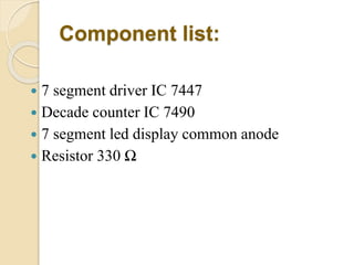
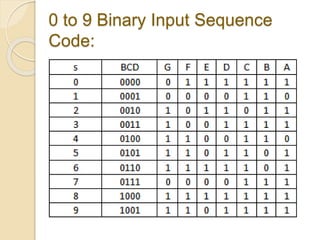
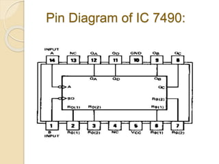
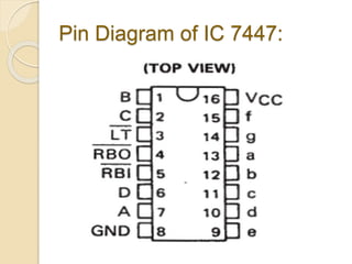
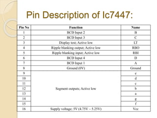
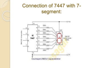
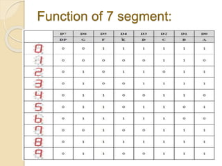
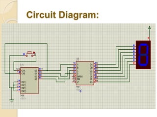
BCD to 7-segment display using IC 7490 and IC 7447
Gujarat Technological University
Prepared By:
Sanchela Maulik M. :- 14EC038
Bhatt Abhay N. :- 14EC022
B. E. (E. & C.)3rd Sem.
BHGCET, Rajkot
Internal Guide:
Prof. Manish P. Patel
Assistant Professor
E & C Dept.
BHGCET, Rajkot
Presentation of Active Learning Assignment
1
Outline:
 Introduction
 Component List
 Pin Diagrams and Descriptions
 Circuit Diagram and Description
 Practical circuit
 References
2
Introduction:
 In our project, using IC7447 and IC7490
we can convert the BCD to 7 segment.
 This project is used in displays, entry
counters, etc.
 When we apply 1 clock pulse at that time
IC7490 generates 4bit BCD code, and it’s
given to IC7447, and finally its displays in
& 7-segment display.
Component list:
 7 segment driver IC 7447
 Decade counter IC 7490
 7 segment led display common anode
 Resistor 330 Ω
0 to 9 Binary Input Sequence
Code:
Pin Diagrams & Description:
Pin Diagram of IC 7490:
Pin Description of IC7490:
Pin No Function Name
1 Clock input 2 Input2
2 Reset1 R(0)1
3 Reset2 R(0)2
4 Not connected NC
5 Supply voltage; 5V (4.75V – 5.25V) Vcc
6 Reset3 R(9)3
7 Reset4 R(9)4
8 Output 3, BCD Output bit 2
QC
9
Output 2, BCD Output bit 1
QB
10 Ground (0V) Ground
11 Output 4, BCD Output bit 3
QD
12 Output 1, BCD Output bit 0
QA
13 Not connected NC
14 Clock input 1 Input1
Pin Diagram of IC 7447:
Pin Description of Ic7447:
Pin No Function Name
1 BCD Input 2 B
2 BCD Input 3 C
3 Display test; Active low LT
4 Ripple blanking output; Active low RBO
5 Ripple blanking input; Active low RBI
6 BCD Input 4 D
7 BCD Input 1 A
8 Ground (0V) Ground
9
Segment outputs; Active low
e
10 d
11 c
12 b
13 a
14 g
15 f
16 Supply voltage; 5V (4.75V – 5.25V) Vcc
Pin Diagram of 7- segment
common anode display:
Types of 7-segment Display:
Connection of 7447 with 7-
segment:
Pin Description of 7- segment
Display:
Function of 7 segment:
Circuit Diagram:
Circuit Diagram Description:
 Pins R0(1), R0(2), R9(1), R9(2) connected to
ground.
 Pins Q0, Q1, Q2, Q3 connected to the output
logic indicator pins of input IC7447 at A, B, C,
D.
 Clk B pin connected to Q0.
 Clk A pin connected to push button for the
input signal ground.
 Output pins of IC7447 Qa, Qb, Qc, Qd, Qe,
Qf, Qg connected to the 7- Segment Display.
 Apply 5 v Vcc Supply to the 7- Segment
Practical Circuit:
References:
 www.davidswinscoe.com/electronics/c
omponents
 www.engineersgarage.com
 www.electroschmetics.com
 www.mouser.in/embedded-solutions/
 www.electronics-tutorials.ws/
20

Bcd to 7 segment display

  • 1.
    BCD to 7-segmentdisplay using IC 7490 and IC 7447 Gujarat Technological University Prepared By: Sanchela Maulik M. :- 14EC038 Bhatt Abhay N. :- 14EC022 B. E. (E. & C.)3rd Sem. BHGCET, Rajkot Internal Guide: Prof. Manish P. Patel Assistant Professor E & C Dept. BHGCET, Rajkot Presentation of Active Learning Assignment 1
  • 2.
    Outline:  Introduction  ComponentList  Pin Diagrams and Descriptions  Circuit Diagram and Description  Practical circuit  References 2
  • 3.
    Introduction:  In ourproject, using IC7447 and IC7490 we can convert the BCD to 7 segment.  This project is used in displays, entry counters, etc.  When we apply 1 clock pulse at that time IC7490 generates 4bit BCD code, and it’s given to IC7447, and finally its displays in & 7-segment display.
  • 4.
    Component list:  7segment driver IC 7447  Decade counter IC 7490  7 segment led display common anode  Resistor 330 Ω
  • 5.
    0 to 9Binary Input Sequence Code:
  • 6.
    Pin Diagrams &Description:
  • 7.
  • 8.
    Pin Description ofIC7490: Pin No Function Name 1 Clock input 2 Input2 2 Reset1 R(0)1 3 Reset2 R(0)2 4 Not connected NC 5 Supply voltage; 5V (4.75V – 5.25V) Vcc 6 Reset3 R(9)3 7 Reset4 R(9)4 8 Output 3, BCD Output bit 2 QC 9 Output 2, BCD Output bit 1 QB 10 Ground (0V) Ground 11 Output 4, BCD Output bit 3 QD 12 Output 1, BCD Output bit 0 QA 13 Not connected NC 14 Clock input 1 Input1
  • 9.
  • 10.
    Pin Description ofIc7447: Pin No Function Name 1 BCD Input 2 B 2 BCD Input 3 C 3 Display test; Active low LT 4 Ripple blanking output; Active low RBO 5 Ripple blanking input; Active low RBI 6 BCD Input 4 D 7 BCD Input 1 A 8 Ground (0V) Ground 9 Segment outputs; Active low e 10 d 11 c 12 b 13 a 14 g 15 f 16 Supply voltage; 5V (4.75V – 5.25V) Vcc
  • 11.
    Pin Diagram of7- segment common anode display:
  • 12.
  • 13.
    Connection of 7447with 7- segment:
  • 14.
    Pin Description of7- segment Display:
  • 15.
    Function of 7segment:
  • 16.
  • 17.
    Circuit Diagram Description: Pins R0(1), R0(2), R9(1), R9(2) connected to ground.  Pins Q0, Q1, Q2, Q3 connected to the output logic indicator pins of input IC7447 at A, B, C, D.  Clk B pin connected to Q0.  Clk A pin connected to push button for the input signal ground.  Output pins of IC7447 Qa, Qb, Qc, Qd, Qe, Qf, Qg connected to the 7- Segment Display.  Apply 5 v Vcc Supply to the 7- Segment
  • 18.
  • 19.
    References:  www.davidswinscoe.com/electronics/c omponents  www.engineersgarage.com www.electroschmetics.com  www.mouser.in/embedded-solutions/  www.electronics-tutorials.ws/
  • 20.