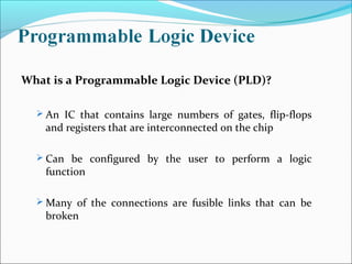
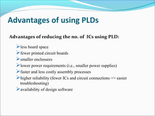
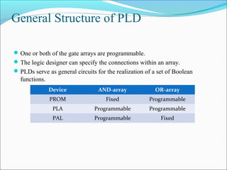
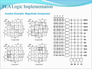
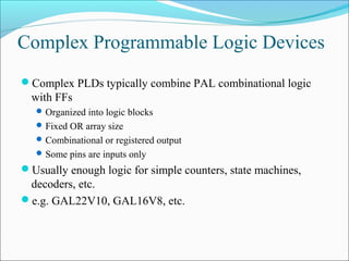
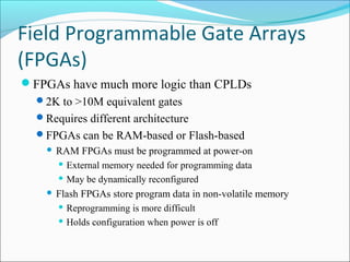
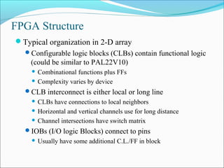
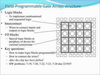
What is a Programmable Logic Device (PLD)?
 An IC that contains large numbers of gates, flip-flops
and registers that are interconnected on the chip
 Can be configured by the user to perform a logic
function
 Many of the connections are fusible links that can be
broken
Advantages of using PLDs
Advantages of reducing the no. of ICs using PLD:
less board space
fewer printed circuit boards
smaller enclosures
lower power requirements (i.e., smaller power supplies)
faster and less costly assembly processes
higher reliability (fewer ICs and circuit connections => easier
troubleshooting)
availability of design software
General Structure of PLD
One or both of the gate arrays are programmable.
The logic designer can specify the connections within an array.
PLDs serve as general circuits for the realization of a set of Boolean
functions.
Device AND-array OR-array
PROM Fixed Programmable
PLA Programmable Programmable
PAL Programmable Fixed
Simplified notation. Each gate has only a single input line.
Inputs are indicated by lines at right angles to the single
gate lines.
A cross at the intersection denotes a fusible link is intact.
PLD Notation
Lack of cross indicates the fuse is blown or no
connection exists.
Example:
Equations
Personality Matrix
1 = asserted in term
0 = negated in term
- = does not participate
1 = term connected to output
0 = no connection to output
Input Side:
Output Side:
F1
1
0
1
0
0
OutputsInputsProduct
term A
1
-
1
-
1
B
1
0
-
0
-
C
-
1
0
0
-
F0
0
0
0
1
1
F2
1
0
0
1
0
F3
0
1
0
0
1
A B
B C
A C
B C
A
F0 = A + B C
F1 = A C + A B
F2 = B C + A B
F3 = B C + A
Example Continued - Unprogrammed device
All possible connections are available
before programming
A B C
F0 F1 F2 F3
Example Continued -
Programmed part Unwanted connections are "blown"
Note: some array structures
work by making connections
rather than breaking them
A B C
F0 F1 F2 F3
AB
BC
AC
BC
A
Alternative representation
Short-hand notation
so we don't have to
draw all the wires!
X at junction indicates
a connection
Notation for implementing
F0 = A B + A B
F1 = C D + C D
A B C D
AB+AB CD+CD
AB
CD
CD
AB
Unprogrammed device
Programmed device
Design Example
F1 = A B C
F2 = A + B + C
F3 = A B C
F4 = A + B + C
F5 = A ⊕ B ⊕ C
F6 = A ⊕ B ⊕ C
Multiple functions of A, B, C
ABC
A
B
C
A
B
C
ABC
ABC
ABC
ABC
ABC
ABC
ABC
F1 F2 F3 F4 F5 F6
A B C
What is difference between Programmable Array Logic (PAL) and
Programmable Logic Array (PLA)?
PAL concept — implemented by Monolithic Memories
AND array is programmable, OR array is fixed at fabrication
A given column of the OR array
has access to only a subset of
the possible product terms
PLA concept — Both AND and OR arrays are programmable
PALs and PLAs
Of the two organizations the PLA is the most flexible
One PLA can implement a huge range of logic functions
BUT many pins; large package, higher cost
PALs are more restricted / you trade number of OR terms vs
number of outputs
Many device variations needed
Each device is cheaper than a PLA
Design Example: BCD to Gray Code Converter
Truth Table
K-maps
Minimized Functions:
A
0
0
0
0
0
0
0
0
1
1
1
1
1
1
1
1
B
0
0
0
0
1
1
1
1
0
0
0
0
1
1
1
1
C
0
0
1
1
0
0
1
1
0
0
1
1
0
0
1
1
D
0
1
0
1
0
1
0
1
0
1
0
1
0
1
0
1
W
0
0
0
0
0
1
1
1
1
1
X
X
X
X
X
X
X
0
0
0
0
1
1
0
0
0
0
X
X
X
X
X
X
Y
0
0
1
1
1
1
1
1
0
0
X
X
X
X
X
X
Z
0
1
1
0
0
0
0
1
1
0
X
X
X
X
X
X
AB
CD 00 01 11 10
00
01
11
10
D
B
C
A
0 0 X 1
0 1 X 1
0 1 X X
0 1 X X
K-map forW
AB
CD 00 01 11 10
00
01
11
10
D
B
C
A
0 1 X 0
0 1 X 0
0 0 X X
0 0 X X
K-map forX
AB
CD 00 01 11 10
00
01
11
10
D
B
C
A
0 1 X 0
0 1 X 0
1 1 X X
1 1 X X
K-map forY
AB
CD 00 01 11 10
00
01
11
10
D
B
C
A
0 0 X 1
1 0 X 0
0 1 X X
1 0 X X
K-map forZ
W = A + B D + B C
X = B C
Y = B + C
Z = A B C D + B C D + A D + B C D
Programmed PAL:
4 product terms per each OR gate
Minimized Functions:
W = A + B D + B C
X = B C
Y = B + C
Z = A B C D + B C D + A D + B C D
A B C D
A B C D
A
BD
BC
0
0
0
0
B
C
0
0
BC
BCD
AD
BCD
W X Y Z
Another Example: Magnitude Comparator
A
K-map forEQ
1 0 0 0
0 1 0 0
0 0 1 0
0 0 0 1
AB
CD 00 01 11 10
00
01
11
10
D
B
C
AB
CD 00 01 11 10
00
01
11
10
D
B
C
A
0 1 1 1
0 0 1 1
0 0 0 0
0 0 1 0
K-map forGT
AB
CD 00 01 11 10
00
01
11
10
D
B
C
A
0 0 0 0
1 0 0 0
1 1 0 1
1 1 0 0
K-map forLT
0 1 1 1
1 0 1 1
1 1 0 1
1 1 1 0
AB
CD 00 01 11 10
00
01
11
10
D
B
C
K-map forNE
A
EQ NE LT GT
ABCD
ABCD
ABCD
ABCD
AC
AC
BD
BD
ABD
BCD
ABC
BCD
A B C D
Complex Programmable Logic Devices
Complex PLDs typically combine PAL combinational logic
with FFs
Organized into logic blocks
Fixed OR array size
Combinational or registered output
Some pins are inputs only
Usually enough logic for simple counters, state machines,
decoders, etc.
e.g. GAL22V10, GAL16V8, etc.
Field Programmable Gate Arrays
(FPGAs)
FPGAs have much more logic than CPLDs
2K to >10M equivalent gates
Requires different architecture
FPGAs can be RAM-based or Flash-based
 RAM FPGAs must be programmed at power-on
 External memory needed for programming data
 May be dynamically reconfigured
 Flash FPGAs store program data in non-volatile memory
 Reprogramming is more difficult
 Holds configuration when power is off
FPGA Structure
Typical organization in 2-D array
Configurable logic blocks (CLBs) contain functional logic
(could be similar to PAL22V10)
 Combinational functions plus FFs
 Complexity varies by device
CLB interconnect is either local or long line
 CLBs have connections to local neighbors
 Horizontal and vertical channels use for long distance
 Channel intersections have switch matrix
IOBs (I/O logic Blocks) connect to pins
 Usually have some additional C.L./FF in block
• Logic blocks
– To implement combinational
and sequential logic
• Interconnect
– Wires to connect inputs and
outputs to logic blocks
• I/O blocks
– Special logic blocks at
periphery of device for
external connections
• Key questions:
– How to make logic blocks programmable?
– How to connect the wires?
– After the chip has been fabbed
– HW problems: 7-19, 7-20, 7-22, 7-23, 7-26 due 22/9/07

Dld ppt

  • 1.
    What is aProgrammable Logic Device (PLD)?  An IC that contains large numbers of gates, flip-flops and registers that are interconnected on the chip  Can be configured by the user to perform a logic function  Many of the connections are fusible links that can be broken
  • 2.
    Advantages of usingPLDs Advantages of reducing the no. of ICs using PLD: less board space fewer printed circuit boards smaller enclosures lower power requirements (i.e., smaller power supplies) faster and less costly assembly processes higher reliability (fewer ICs and circuit connections => easier troubleshooting) availability of design software
  • 3.
    General Structure ofPLD One or both of the gate arrays are programmable. The logic designer can specify the connections within an array. PLDs serve as general circuits for the realization of a set of Boolean functions. Device AND-array OR-array PROM Fixed Programmable PLA Programmable Programmable PAL Programmable Fixed
  • 4.
    Simplified notation. Eachgate has only a single input line. Inputs are indicated by lines at right angles to the single gate lines. A cross at the intersection denotes a fusible link is intact. PLD Notation
  • 5.
    Lack of crossindicates the fuse is blown or no connection exists.
  • 6.
    Example: Equations Personality Matrix 1 =asserted in term 0 = negated in term - = does not participate 1 = term connected to output 0 = no connection to output Input Side: Output Side: F1 1 0 1 0 0 OutputsInputsProduct term A 1 - 1 - 1 B 1 0 - 0 - C - 1 0 0 - F0 0 0 0 1 1 F2 1 0 0 1 0 F3 0 1 0 0 1 A B B C A C B C A F0 = A + B C F1 = A C + A B F2 = B C + A B F3 = B C + A
  • 7.
    Example Continued -Unprogrammed device All possible connections are available before programming A B C F0 F1 F2 F3
  • 8.
    Example Continued - Programmedpart Unwanted connections are "blown" Note: some array structures work by making connections rather than breaking them A B C F0 F1 F2 F3 AB BC AC BC A
  • 9.
    Alternative representation Short-hand notation sowe don't have to draw all the wires! X at junction indicates a connection Notation for implementing F0 = A B + A B F1 = C D + C D A B C D AB+AB CD+CD AB CD CD AB Unprogrammed device Programmed device
  • 10.
    Design Example F1 =A B C F2 = A + B + C F3 = A B C F4 = A + B + C F5 = A ⊕ B ⊕ C F6 = A ⊕ B ⊕ C Multiple functions of A, B, C ABC A B C A B C ABC ABC ABC ABC ABC ABC ABC F1 F2 F3 F4 F5 F6 A B C
  • 11.
    What is differencebetween Programmable Array Logic (PAL) and Programmable Logic Array (PLA)? PAL concept — implemented by Monolithic Memories AND array is programmable, OR array is fixed at fabrication A given column of the OR array has access to only a subset of the possible product terms PLA concept — Both AND and OR arrays are programmable
  • 12.
    PALs and PLAs Ofthe two organizations the PLA is the most flexible One PLA can implement a huge range of logic functions BUT many pins; large package, higher cost PALs are more restricted / you trade number of OR terms vs number of outputs Many device variations needed Each device is cheaper than a PLA
  • 13.
    Design Example: BCDto Gray Code Converter Truth Table K-maps Minimized Functions: A 0 0 0 0 0 0 0 0 1 1 1 1 1 1 1 1 B 0 0 0 0 1 1 1 1 0 0 0 0 1 1 1 1 C 0 0 1 1 0 0 1 1 0 0 1 1 0 0 1 1 D 0 1 0 1 0 1 0 1 0 1 0 1 0 1 0 1 W 0 0 0 0 0 1 1 1 1 1 X X X X X X X 0 0 0 0 1 1 0 0 0 0 X X X X X X Y 0 0 1 1 1 1 1 1 0 0 X X X X X X Z 0 1 1 0 0 0 0 1 1 0 X X X X X X AB CD 00 01 11 10 00 01 11 10 D B C A 0 0 X 1 0 1 X 1 0 1 X X 0 1 X X K-map forW AB CD 00 01 11 10 00 01 11 10 D B C A 0 1 X 0 0 1 X 0 0 0 X X 0 0 X X K-map forX AB CD 00 01 11 10 00 01 11 10 D B C A 0 1 X 0 0 1 X 0 1 1 X X 1 1 X X K-map forY AB CD 00 01 11 10 00 01 11 10 D B C A 0 0 X 1 1 0 X 0 0 1 X X 1 0 X X K-map forZ W = A + B D + B C X = B C Y = B + C Z = A B C D + B C D + A D + B C D
  • 14.
    Programmed PAL: 4 productterms per each OR gate Minimized Functions: W = A + B D + B C X = B C Y = B + C Z = A B C D + B C D + A D + B C D A B C D A B C D A BD BC 0 0 0 0 B C 0 0 BC BCD AD BCD W X Y Z
  • 15.
    Another Example: MagnitudeComparator A K-map forEQ 1 0 0 0 0 1 0 0 0 0 1 0 0 0 0 1 AB CD 00 01 11 10 00 01 11 10 D B C AB CD 00 01 11 10 00 01 11 10 D B C A 0 1 1 1 0 0 1 1 0 0 0 0 0 0 1 0 K-map forGT AB CD 00 01 11 10 00 01 11 10 D B C A 0 0 0 0 1 0 0 0 1 1 0 1 1 1 0 0 K-map forLT 0 1 1 1 1 0 1 1 1 1 0 1 1 1 1 0 AB CD 00 01 11 10 00 01 11 10 D B C K-map forNE A EQ NE LT GT ABCD ABCD ABCD ABCD AC AC BD BD ABD BCD ABC BCD A B C D
  • 16.
    Complex Programmable LogicDevices Complex PLDs typically combine PAL combinational logic with FFs Organized into logic blocks Fixed OR array size Combinational or registered output Some pins are inputs only Usually enough logic for simple counters, state machines, decoders, etc. e.g. GAL22V10, GAL16V8, etc.
  • 17.
    Field Programmable GateArrays (FPGAs) FPGAs have much more logic than CPLDs 2K to >10M equivalent gates Requires different architecture FPGAs can be RAM-based or Flash-based  RAM FPGAs must be programmed at power-on  External memory needed for programming data  May be dynamically reconfigured  Flash FPGAs store program data in non-volatile memory  Reprogramming is more difficult  Holds configuration when power is off
  • 18.
    FPGA Structure Typical organizationin 2-D array Configurable logic blocks (CLBs) contain functional logic (could be similar to PAL22V10)  Combinational functions plus FFs  Complexity varies by device CLB interconnect is either local or long line  CLBs have connections to local neighbors  Horizontal and vertical channels use for long distance  Channel intersections have switch matrix IOBs (I/O logic Blocks) connect to pins  Usually have some additional C.L./FF in block
  • 19.
    • Logic blocks –To implement combinational and sequential logic • Interconnect – Wires to connect inputs and outputs to logic blocks • I/O blocks – Special logic blocks at periphery of device for external connections • Key questions: – How to make logic blocks programmable? – How to connect the wires? – After the chip has been fabbed – HW problems: 7-19, 7-20, 7-22, 7-23, 7-26 due 22/9/07