Combinational and sequential logic
•
7 likes•1,730 views

Combinational circuits - Half adder, Full Adder, Parallel binary adder, Subtracter, Magnitude Comparator, Decoders, Encoders, Multiplexers, Demultiplexers, Parity bit generator, PLA. Sequential circuits - Flip Flops – RS, JK, T and D Flip Flops, Edge triggered Flip Flops, Master slave Flip Flops.

Recommended
More Related Content
What's hot
What's hot (20)
Viewers also liked
Viewers also liked (19)
Similar to Combinational and sequential logic
Similar to Combinational and sequential logic (20)
More from Deepak John
More from Deepak John (20)
Recently uploaded
Recently uploaded (20)
Combinational and sequential logic
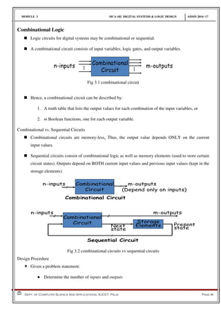
- 1. MODULE 3 MCA-102 DIGITAL SYSTEMS & LOGIC DESIGN ADMN 2014-‘17 Dept. of Computer Science And Applications, SJCET, Palai Page 46 Combinational Logic Logic circuits for digital systems may be combinational or sequential. A combinational circuit consists of input variables, logic gates, and output variables. Fig 3.1 combinational circuit Hence, a combinational circuit can be described by: 1. A truth table that lists the output values for each combination of the input variables, or 2. m Boolean functions, one for each output variable. Combinational vs. Sequential Circuits Combinational circuits are memory-less. Thus, the output value depends ONLY on the current input values. Sequential circuits consist of combinational logic as well as memory elements (used to store certain circuit states). Outputs depend on BOTH current input values and previous input values (kept in the storage elements). Fig 3.2 combinational circuits vs sequential circuits Design Procedure Given a problem statement: ● Determine the number of inputs and outputs
- 2. MODULE 3 MCA-102 DIGITAL SYSTEMS & LOGIC DESIGN ADMN 2014-‘17 Dept. of Computer Science And Applications, SJCET, Palai Page 47 ● Derive the truth table ● Simplify the Boolean expression for each output ● Produce the required circuit Half Adder A combinational circuit that performs the addition of two bits is called a half adder. Fig 3.3 logical symbol of half adder The truth table for the half adder is listed below: x y C S 0 0 0 0 0 1 0 1 1 0 0 1 1 1 1 0 Fig 3.3 truth table for half adder S = x’y + xy’ C = xy Fig 3.4 half adder logic diagram
- 3. MODULE 3 MCA-102 DIGITAL SYSTEMS & LOGIC DESIGN ADMN 2014-‘17 Dept. of Computer Science And Applications, SJCET, Palai Page 48 Full Adder One that performs the addition of three bits (two significant bits and a previous carry) is a full adder. x y z C S 0 0 0 0 0 0 0 1 0 1 0 1 0 0 1 0 1 1 1 0 1 0 0 0 1 1 0 1 1 0 1 1 0 1 0 1 1 1 1 1 Fig 3.5 truth table for full adder Fig 3.6 maps for full adder S = x’y’z + x’yz’ + xy’z’ + xyz C = xy + xz + yz Alternative formulae using algebraic manipulation: C = X.Y + X.Z + Y.Z = X.Y + (X + Y).Z = X.Y + ((X XOR Y) + X.Y).Z = X.Y + (X XOR Y).Z + X.Y.Z = X.Y + (X XOR Y).Z
- 4. MODULE 3 MCA-102 DIGITAL SYSTEMS & LOGIC DESIGN ADMN 2014-‘17 Dept. of Computer Science And Applications, SJCET, Palai Page 49 S = X'.Y'.Z + X'.Y.Z' + X.Y'.Z' + X.Y.Z = X‘. (Y'.Z + Y.Z') + X. (Y'.Z' + Y.Z) = X'. (Y XOR Z) + X. (Y XOR Z)' = X XOR (Y XOR Z) or (X XOR Y) XOR Z Fig 3.7 full adder logic diagram Fig 3.8 Full adder using two half adder Parallel Binary Adders • Parallel Adder is a digital circuit that produces the arithmetic sum of 2 binary numbers. • Constructed with full adders connected in cascade, with output carry from each full adder connected to the input carry of next full adder in the chain. • The carries are connected in a chain through the full adders. • Two methods to handle carries in parallel adder 1. Ripple carry: carry out of each FA is connected to the carry input of next FA 2. Carry Look ahead: it anticipates the output carry of each stage, and based on the input bits of each stage, produces the output carry by either carry generation or carry propagation.
- 5. MODULE 3 MCA-102 DIGITAL SYSTEMS & LOGIC DESIGN ADMN 2014-‘17 Dept. of Computer Science And Applications, SJCET, Palai Page 50 Carry generation: output carry is produced internally by the FA.carry is generated only when both input bits are 1s.the generated carry C is expressed as the AND function of two input bits A and B so C=AB. Carry propagation: occurs when the i/p carry is rippled to become the o/p carry.an i/p carry may be propagated by the full adder when either or both of the i/p bits are 1s.the propagated carry Cp is expressed as the OR function of the i/p bits ie Cp=A+B 2- Bit Parallel Adder • LSB of two binary numbers are represented by A1 and B1. • The next higher bit are A2 and B2. The resulting t 1 2 and CO, in which the CO becomes MSB. • The carry output CO of each adder is connected as the carry input of the next higher order. Fig 3.9 2bit adder using two full adder Four Bit Parallel Adders • An n-bit adder requires n full adders with each output connected to the input carry of the next higher-order full adder. • The carry output of each adder is connected to the carry input of next adder called as internal carries. A2A1 + B2B1 C0 ∑2 ∑1
- 6. MODULE 3 MCA-102 DIGITAL SYSTEMS & LOGIC DESIGN ADMN 2014-‘17 Dept. of Computer Science And Applications, SJCET, Palai Page 51 Fig 3.10 4 bit adder The logic symbol for a 4-bit parallel adder is shown. This 4-bit adder includes a Carry In (labeled C0) and a Carry Out (labeled C4). Fig 3.11 truth table for 4 bit parallel adder 74283 Four-bit binary adder 7483 is an older chip that is functionally identical to the 74283, but the pins are laid out differently Cascading Parallel Adders When we connect the outputs from one circuit to the inputs of another identical circuit to expand the number of bits being operated on, we say that the circuits are cascaded together. For example, you can cascade two 4-bit parallel adders to add two 8-bit numbers. To do this, connect the lower-order adder’s Carry Out to the higher-order adder’s Carry In.
- 7. MODULE 3 MCA-102 DIGITAL SYSTEMS & LOGIC DESIGN ADMN 2014-‘17 Dept. of Computer Science And Applications, SJCET, Palai Page 52 Fig 3.12 cascading of parallel adders Binary Subtraction • The subtraction A-B can be performed by taking the 2's complement of B and adding to A. • The 2's complement of B can be obtained by complementing B and adding one to the result. A-B = A + 2C(B) = A + 1C(B) + 1 = A + B’ + 1 Fig 3.13 binary substractor circuit Adder/Substractor Design requires: (i) XOR gates:
- 8. MODULE 3 MCA-102 DIGITAL SYSTEMS & LOGIC DESIGN ADMN 2014-‘17 Dept. of Computer Science And Applications, SJCET, Palai Page 53 (ii) S connected to carry-in. Fig 3.14 adder/substractor circuit • When S=0, the circuit performs A + B. The carry in is 0, and the XOR gates simply pass B untouched. • When S=1, the carry into the least significant bit (LSB) is 1, and B is complemented (1’s complement) prior to the addition; hence, the circuit adds to A the 1’s complement of B plus 1 (from the carry into the LSB). Magnitude Comparator A magnitude comparator is a combinational circuit that compares two numbers, A and B, and then determines their relative magnitudes. A > B A = B A < B Fig 3.15 logical symbol of magnitude comparator Problem: Design a magnitude comparator that compares 2 4-bit numbers A and B and determines whether: A > B, or A = B, or A < B Inputs First n-bit number A
- 9. MODULE 3 MCA-102 DIGITAL SYSTEMS & LOGIC DESIGN ADMN 2014-‘17 Dept. of Computer Science And Applications, SJCET, Palai Page 54 Second n-bit number B Outputs 3 output signals (GT, EQ, LT), where: GT = 1 IFF A > B EQ = 1 IFF A = B LT = 1 IFF A < B Exactly One of these 3 outputs equals 1, while the other 2 outputs are 0`s. Solution: Inputs: 8-bits (A ⇒ 4-bits, B ⇒ 4-bits).A and B are two 4-bit numbers. Let A = A3A2A1A0, and Let B = B3B2B1B0 . Design of the EQ Define Xi = Ai xnor Bi = Ai Bi + Ai’ Bi’ i = 1 IFF Ai = Bi ∀ i =0, 1, 2 and 3 i = 0 IFF Ai ≠ Bi Therefore the condition for A = B or EQ=1 IFF A3= B3 → (X3 = 1), and A2= B2 → (X2 = 1), and A1= B1 → (X1 = 1), and A0= B0 → (X0 = 1). Thus, EQ=1 IFF X3 X2 X1 X0 = 1. In other words, EQ = X3 X2 X1 X0 Designing GT and LT: GT = 1 if A > B: If A3 > B3 3 = 1 and B3 = 0 If A3 = B3 and A2 > B2 If A3 = B3 and A2 = B2 and A1 > A1 If A3 = B3 and A2 = B2 and A1 = B1 and A0 > B0 Therefore, GT = A3B3‘+ X3 A2 B2‘+ X3 X2 A1 B1‘+ X3 X2 X1A0 B0‘ Similarly, LT = A3’B3 + X3 A2‘B2 + X3 X2 A1’B1 + X3 X2 X1A0’ B0
- 10. MODULE 3 MCA-102 DIGITAL SYSTEMS & LOGIC DESIGN ADMN 2014-‘17 Dept. of Computer Science And Applications, SJCET, Palai Page 55 Fig 3.16 4 bit magnitude comparator Decoder • A decoder is a logic circuit that accepts a set of inputs that represents a binary number and activates only the output that corresponds to the input number. • A decoder has • N inputs • 2N outputs • Exactly one output will be active for each combination of the inputs. Fig 3.17 logical symbol of N-M decoder • For each of these input combinations only one of the M outputs will be active HIGH (1), all the other outputs are LOW (0). An AND gate can be used as the basic decoding element because it produces a HIGH output only when all inputs are HIGH.
- 11. MODULE 3 MCA-102 DIGITAL SYSTEMS & LOGIC DESIGN ADMN 2014-‘17 Dept. of Computer Science And Applications, SJCET, Palai Page 56 • If an active-LOW output (74138, one of the output will low and the rest will be high) is required for each decoded number, the entire decoder can be implemented with NAND gates Inverters • If an active-HIGH output (74139, one of the output will high and the rest will be low) is required for each decoded number, the entire decoder can be implemented with AND gates Inverters Decoder example 2-to-4-Line Decoder Fig 3.18 2-4 decoder with active high output Fig 3.19 logical symbol and truth table of 2-4 decoder in fig 3.19 3-8 line decoder (active-HIGH) • It can be called a 3-line-to- 8-line decoder, because it has three input lines and eight output lines. • It could also be called a binary-octal decoder or converters because it takes a three bit binary input code and activates the one of the eight outputs corresponding to that code. It is also referred to as a 1-of-8 decoder, because only 1 of the 8 outputs is activated at one time.
- 12. MODULE 3 MCA-102 DIGITAL SYSTEMS & LOGIC DESIGN ADMN 2014-‘17 Dept. of Computer Science And Applications, SJCET, Palai Page 57 Fig 3.20 3-8 decoder circuit Fig 3.21 truth table for circuit in fig 3.21 Application example A simplified computer I/O port system with a port address decoder with only four address lines shown.
- 13. MODULE 3 MCA-102 DIGITAL SYSTEMS & LOGIC DESIGN ADMN 2014-‘17 Dept. of Computer Science And Applications, SJCET, Palai Page 58 Fig 3.22 peripheral decoding in computer • Computer must communicate with a variety of external devices called peripherals by sending and/or receiving data through what is known as input/output (I/O) ports • Each I/O port has a number, called an address, which uniquely identifies it. When the computer wants to communicate with a particular device, it issues the appropriate address code for the I/O port to which that particular device is connected. The binary port address is decoded and appropriate decoder output is activated to enable the I/O port • Binary data are transferred within the computer on a data bus, which is a set of parallel lines BCD -to- Decimal decoders • The BCD- to-decimal decoder converts each BCD code into one of Ten Positional decimal digit indications. It is frequently referred as a 4-line -to- 10 line decoder • The method of implementation is that only ten decoding gates are required because the BCD code represents only the ten decimal digits 0 through 9. • Each of these decoding functions is implemented with NAND gates to provide active -LOW outputs. If an active HIGH output is required, AND gates are used for decoding
- 14. MODULE 3 MCA-102 DIGITAL SYSTEMS & LOGIC DESIGN ADMN 2014-‘17 Dept. of Computer Science And Applications, SJCET, Palai Page 59 Fig 3. 23 a. logic circuit for BCD to Decimal decoder b. logical symbol of BCD to Decimal decoder IC c. truth table BCD to 7-Segment Display Decoder Used to convert a BCD or a binary code into a 7 segment code used to operate a 7 segment LED display. It generally has 4 input lines and 7 output lines. Here we design a simple display decoder circuit using logic gates. Fig 3.24 logical symbol of BCD-7 segment decoder
- 15. MODULE 3 MCA-102 DIGITAL SYSTEMS & LOGIC DESIGN ADMN 2014-‘17 Dept. of Computer Science And Applications, SJCET, Palai Page 60 Encoder Encoders typically have 2N inputs and N outputs. These are called 2N–to–N encoders. Encoders can also be devised to encode various symbols and alphabetic characters. The process of converting from familiar symbols or numbers to a coded format is called encoding. Fig 3.25 Logical diagram of Encoder 8-to-3 encoder Implementation Octal-to-Binary An octal to binary encoder has 23 = 8 input lines D0 to D7 and 3 output lines Y0 to Y2. Below is the truth table for an octal to binary encoder. Fig 3. 26 truth table for 8-3 encoder From the truth table, the outputs can be expressed by following Boolean Function. Y0 = D1 + D3 + D5 + D7
- 16. MODULE 3 MCA-102 DIGITAL SYSTEMS & LOGIC DESIGN ADMN 2014-‘17 Dept. of Computer Science And Applications, SJCET, Palai Page 61 Y1 = D2 + D3 + D6 + D7 Y2 = D4 + D5 + D6 + D7 Note: Above boolean functions are formed by ORing all the input lines for which output is 1. For instance Y0 is 1 for D1, D3, D5, D7 input lines. The encoder can therefore be implemented with OR gates whose inputs are determined directly from truth table as shown in the image below: Fig 3.27 logic circuit for 8-3 encoder Decimal – BCD encoder • Encoder will produce a BCD output corresponding to the highest-order decimal digit input that is active and will ignore any other lower order active inputs. Fig 3.28 truth table for 10-4 encoder From the truth table, the outputs can be expressed by following Boolean Function. Note: Below Boolean functions are formed by OR ing all the input lines for which output is 1. For instance A0 is 1 for 1,3,5,7 or 9 input lines. A0 = 1+3+5+7+9
- 17. MODULE 3 MCA-102 DIGITAL SYSTEMS & LOGIC DESIGN ADMN 2014-‘17 Dept. of Computer Science And Applications, SJCET, Palai Page 62 A1 = 2+3+6+7 A2 = 4+5+6+7 A3 = 8+9 The decimal to bcd encoder can therefore be implemented with OR gates whose inputs are determined directly from truth table as shown in the image below. Fig 3.29 Logic circuit and symbol for 10-4 encoder Multiplexer A multiplexer or mux is a device that selects one of several analog or digital input signals and forwards the selected input into a single line. A multiplexer of 2n inputs has n select lines, which are used to select which input line to send to the output.” The select lines determine which input is connected to the output. MUX Types -to-1 (1 select line) -to-1 (2 select lines) -to-1 (3 select lines) -to-1 (4 select lines)
- 18. MODULE 3 MCA-102 DIGITAL SYSTEMS & LOGIC DESIGN ADMN 2014-‘17 Dept. of Computer Science And Applications, SJCET, Palai Page 63 Fig 3.30 multiplexer block diagram 4-to-1 Multiplexer (MUX) Fig 3.31 logic circuit, symbol and table for 4-1 multiplexer The Boolean expression for this 4-to-1 Multiplexer above with inputs D0 to D3 and data select lines A, B is given as: Y = A’B’D0 + A’B D1 + AB’D2 + ABD3 Demultiplexer • A DEMUX is a digital switch with a single input (source) and a multiple outputs (destinations). • The select lines determine which output the input is connected to. • DEMUX Types
- 19. MODULE 3 MCA-102 DIGITAL SYSTEMS & LOGIC DESIGN ADMN 2014-‘17 Dept. of Computer Science And Applications, SJCET, Palai Page 64 -to-2 (1 select line) -to-4 (2 select lines) -to-8 (3 select lines) -to-16 (4 select lines) Fig 3.32 Demultiplexer circuit symbol 1-to-4 De-Multiplexer (DEMUX) Fig 3.33 logic circuit for 1-4 demultiplexer, symbol and table Parity Bit Generator The most common error detection code used is the parity bit. A parity bit is an extra bit included with a binary message to make the total number of 1's either odd or even. A parity bit added to n-bit code produces (n+1)-bit code with an odd (or even) count of 1s Odd Parity bit: count of 1s in (n+1)-bit code is odd o So use an even function to generate the odd parity bit Even Parity bit: count of 1s in (n+1)-bit code is even o So use an odd function to generate the even parity bit
- 20. MODULE 3 MCA-102 DIGITAL SYSTEMS & LOGIC DESIGN ADMN 2014-‘17 Dept. of Computer Science And Applications, SJCET, Palai Page 65 To check for odd parity o Use an even function to check the (n+1)-bit code To check for even parity o Use an odd function to check the (n+1)-bit code Even Parity Generators and Checkers for 3-bit codes An even parity bit could be added to n-bit code to produce an n + 1 bit code: • Use an odd function to produce codes with even parity • Use odd function circuit to check code words with even parity Example: n = 3. Generate even parity code words of length 4 with an odd function circuit (parity generator): The design procedure is made simple by writing the truth table for the circuit. Fig 3.34 truth table fon parity bit generator Fig 3.35 K-map for the truth table in fig 3.35 From this the minimal output equation is This function can be implemented using exclusive-or gates, shown in fig 3.37.Similarly the checker circuit can be designed using XOR gates, where
- 21. MODULE 3 MCA-102 DIGITAL SYSTEMS & LOGIC DESIGN ADMN 2014-‘17 Dept. of Computer Science And Applications, SJCET, Palai Page 66 Fig 3.36 even parity generator and checker Operation: (X,Y,Z) = (0,0,1) gives (X,Y,Z,P) = (0,0,1,1) and E = 0.If Y changes from 0 to 1 between generator and checker, then E = 1 indicates an error. Odd Parity Generators and Checkers Similarly, an odd parity bit could be added to n-bit code to produce an n + 1 bit code • Use an even function to produce codes with odd parity • Use even function circuit to check code words with odd parity Message X Y Z Odd Parity Generator P Checker Bit C 0 0 0 1 0 0 0 1 0 0 0 1 0 0 0 0 1 1 1 0 1 0 0 0 0 1 0 1 1 0 1 1 0 1 0 1 1 1 0 0 Fig 3.37 Truth table for Odd parity generator C
- 22. MODULE 3 MCA-102 DIGITAL SYSTEMS & LOGIC DESIGN ADMN 2014-‘17 Dept. of Computer Science And Applications, SJCET, Palai Page 67 1 1 1 1 Fig 3.38 k-map for fig 3.39 From this the minimal output equation is P=X’Y’Z’+X’YZ’+XYZ’+XY’Z This function can be implemented using XOR and XNOR gates, shown in fig 3.40.Similarly the checker circuit can be designed using XOR and XNOR gates, where Fig 3.39 odd parity generator and checker circuit Fig 3.40 Odd parity checker circuit PLA [Programmable Logic Array] Combination of a programmable AND array followed by a programmable OR array. This layout allows for a large number of logic functions to be synthesized in the sum of products (and sometimes product of sums) canonical forms. 00 01 11 10 0 1 Z Y X P Y X C P Z
- 23. MODULE 3 MCA-102 DIGITAL SYSTEMS & LOGIC DESIGN ADMN 2014-‘17 Dept. of Computer Science And Applications, SJCET, Palai Page 68 Fig 3.41 block diagram of PLA Example :Design a PLA to realize the following logic functions f0 (A'.B'+ A. C') f1 (A. C'+ B) f2 (A'.B'+ B. C’) f3 (B+ AC) Fig 3.42 PLA table Fig 3.43 realisation of PLA
- 24. MODULE 3 MCA-102 DIGITAL SYSTEMS & LOGIC DESIGN ADMN 2014-‘17 Dept. of Computer Science And Applications, SJCET, Palai Page 69 Example: Design a PLA to realise the following three logic functions f1 (A, B, C, D, E) = A'.B'.D' + B'.C.D' + A'.B.C.D.E' f2 (A, B, C, D, E) = A'.B.E + B'.C.D'.E f3 (A, B, C, D, E) = A'.B'.D' + B'.C'.D'.E + A'.B.C.D Fig 3.44 realisation of PLA SEQUENTIAL LOGIC CIRCUITS Sequential circuits are constructed using combinational logic and a number of memory elements with some or all of the memory outputs fed back into the combinational logic forming a feedback path or loop. Sequential circuit = Combinational logic + Memory Elements
- 25. MODULE 3 MCA-102 DIGITAL SYSTEMS & LOGIC DESIGN ADMN 2014-‘17 Dept. of Computer Science And Applications, SJCET, Palai Page 70 Fig 3.45 sequential circuit There are two types of sequential circuits: synchronous: outputs change only at specific time asynchronous: outputs change at any time A state variable in a sequential circuit represents the single-bit variable Q stored in a memory element in circuit. – Each memory element may be in state 0 or state 1 depending on the current value stored in the memory element. • The State of A sequential Circuit: – The collection of all state variables (memory element stored values) that at any time contain all the information about the past necessary to account for the circuit’s future behavior. – A sequential circuit that contains n memory elements could be in one of a maximum of 2n states at any given time depending on the stored values in the memory elements. – Sequential Circuit State transition: A change in the stored values in memory elements thus changing the sequential circuit from one state to another. Clock Signals & Synchronous Sequential Circuits • A clock signal is a periodic square wave that indefinitely switches values from 0 to 1 and 1 to 0 at fixed intervals. Clock cycle time or clock period: The time interval between two consecutive rising or falling edges of the clock.
- 26. MODULE 3 MCA-102 DIGITAL SYSTEMS & LOGIC DESIGN ADMN 2014-‘17 Dept. of Computer Science And Applications, SJCET, Palai Page 71 Fig 3.46 clock signal Synchronous Sequential Circuits: Sequential circuits that have a clock signal as one of its inputs: – All state transitions in such circuits occur only when the clock value is either 0 or 1 or happen at the rising or falling edges of the clock depending on the type of memory elements used in the circuit. Sequential Circuit Memory Elements: Latches, Flip-Flops • Latches and flip-flops are the basic single-bit memory elements used to build sequential circuit with one or two inputs/outputs, designed using individual logic gates and feedback loops. • Latches: – The output of a latch depends on its current inputs and on its previous inputs and its change of state can happen at any time when its inputs change. • Flip-Flop: – The output of a flip-flop also depends on current and previous input but the change in output (change of state or state transition) occurs at specific times determined by a clock input. S-R Latch • An S-R (set-reset) latch can be built using two NOR gates forming a feedback loop. • The output of the S-R latch depends on current as well as previous inputs or state, and its state (value stored) can change as soon as its inputs change. When Q is HIGH, the latch is in SET state. When Q is LOW, the latch is in RESET state. Fig 3.47 SR latch circuit diagram, truth table and symbol S R Q Q'
- 27. MODULE 3 MCA-102 DIGITAL SYSTEMS & LOGIC DESIGN ADMN 2014-‘17 Dept. of Computer Science And Applications, SJCET, Palai Page 72 S-R Flip flop Since the S-R latch is responsive to its inputs at all times an enable line C is used to disable or enable state transitions. Behaves similar to a regular S-R latch when enable C=1 Fig 3.48 gated SR flip flop S = 0, R = 0; this is the normal resting state of the circuit and it has no effect of the output states. Q and Q’ will remain in whatever state they were in prior to the occurrence of this input condition. It works in HOLD (no change) mode operation. • S = 0, R = 1; this will reset Q to 0, it works in RESET mode operation. S = 1, R = 0; this will set Q to 1, it works in SET mode operation. S = 1, R = 1; this condition tries to set and reset the NOR gate latch at the same time, and it produces Q = ¯ = 0. This is an unexpected condition and are not used. Since the two outputs should be inverse of each other. If the inputs are returned to 1 simultaneously, the output states are unpredictable. This input condition should not be used and when circuits are constructed, the design should make this condition SET=RESET = 1 never arises. Clocked SR Flip Flop Additional clock input is added to change the SR flip-flop from an element used in asynchronous sequential circuits to one, which can be used in synchronous circuits. Fig 3.49 Clocked SR flip flop Its means that the flip flop can change the output states only when clock signal makes a transition from LOW to HIGH. S EN R Q Q'
- 28. MODULE 3 MCA-102 DIGITAL SYSTEMS & LOGIC DESIGN ADMN 2014-‘17 Dept. of Computer Science And Applications, SJCET, Palai Page 73 Fig 3.50 truth table for clocked SR flip flop Clocked SR Flip Flop Circuit with PRESET and CLEAR Some flip-flops have asynchronous preset Pr and clear Cl signals. Output changes once these signals change, however the input signals must wait for a change in clock to change the output Fig 3.51 SR flip flop with preset and clear JK Flip Flop Another types of Flip flop is JK flip flop. It differs from the RS flip flops when J=K=1 condition is not indeterminate but it is defined to give a very useful changeover (toggle) action. Toggle means that Q and Q ¯ will switch to their opposite states. The JK Flip flop has clock input Cp and two control inputs J and K. Operation of Jk Flip Flop is completely described by truth table Fig 3.52 JK flip flop
- 29. MODULE 3 MCA-102 DIGITAL SYSTEMS & LOGIC DESIGN ADMN 2014-‘17 Dept. of Computer Science And Applications, SJCET, Palai Page 74 JK Flip Flop with preset and clear This flip flop can also have other inputs called Preset (or SET) and clear that can be used for setting the flip Flop to 1 or resetting it to 0 by applying the appropriate signal to the Preset and Clear inputs. These inputs can change the state of the flip flop regardless of synchronous inputs or the clock. Fig 3.53 JK flip flop with PRESET and CLEAR T Flip Flop The T flip flop has only the Toggle and Hold Operation. If Toggle mode operation. The output will toggle from 1 to 0 or vice versa. Fig 3.54 T flip flop
- 30. MODULE 3 MCA-102 DIGITAL SYSTEMS & LOGIC DESIGN ADMN 2014-‘17 Dept. of Computer Science And Applications, SJCET, Palai Page 75 D Flip Flop Also Known as Data Flip flop Can be constructed from RS Flip Flop or JK Flip flop by addition of an inverter. Inverter is connected so that the R input is always the inverse of S (or J input is always complementary of K). The D flip flop will act as a storage element for a single binary digit (Bit). Fig 3.55 D flip flop EDGE TRIGGERED FLIP FLOP Edge triggered flip-flop changes only when the clock C changes The three basic types are introduced here: S-R, J-K and D. Edge-triggered S-R flip-flop The basic operation is illustrated below, along with the truth table for this type of flip-flop. The operation and truth table for a negative edge-triggered flip-flop are the same as those for a positive except that the falling edge of the clock pulse is the triggering edge. As S = 1, R = 0. Flip-flop SETS on the rising clock edge. Fig 3.56 edge triggered SR flip flop Edge-triggered J-K flip-flop The J-K flip-flop works very similar to S-R flip-flop. The only difference is that this flip-flop has NO invalid state. The outputs toggle (change to the opposite state) when both J and K inputs are HIGH.
- 31. MODULE 3 MCA-102 DIGITAL SYSTEMS & LOGIC DESIGN ADMN 2014-‘17 Dept. of Computer Science And Applications, SJCET, Palai Page 76 Edge-triggered D flip-flop The operations of a D flip-flop is much simpler. It has only one input addition to the clock. It is very useful when a single data bit (0 or 1) is to be stored. If there is a HIGH on the D input when a clock pulse is applied, the flip-flop SETs and stores a 1. If there is a LOW on the D input when a clock pulse is applied, the flip-flop RESETs and stores a 0. The truth table below summarize the operations of the positive edge-triggered D flip-flop. As before, the negative edge-triggered flip-flop works the same except that the falling edge of the clock pulse is the triggering edge. MASTER-SLAVE FLIP FLOP Is designed using two separate flip flops. Out of these, one acts as the master and the other as a slave. The figure of a master-slave J-K flip flop is shown below. Fig 3.57 master slave flip flop From the above figure you can see that both the J-K flip flops are presented in a series connection. The output of the master J-K flip flop is fed to the input of the slave J-K flip flop. The output of the slave J-K flip flop is given as a feedback to the input of the master J-K flip flop. The clock pulse [Clk] is given to the master J-K flip flop and it is sent through a NOT Gate and thus inverted before passing it to the slave J-K flip flop. When Clk=1, the master J-K flip flop gets disabled. The Clk input of the master input will be the opposite of the slave input. So the master flip flop output will be recognized by the slave flip flop only when the Clk value becomes 0. Thus, when the clock pulse males a transition from 1 to 0, the locked outputs of the master flip flop are fed through to the inputs of the slave flip-flop making this flip flop edge or pulse-triggered.