The document describes experiments conducted on logic gates. It lists the components needed, provides theory on logic gates like AND, OR, NOT, NAND and NOR gates. It explains the procedure to study the gates and verify their truth tables. Circuits for half adder, full adder, half subtractor, full subtractor and various code converters are designed and their truth tables verified.
DIGITAL ELECTRONICS LAB
Ex.No:1
STUDY OF LOGIC GATES
Date:
AIM:
To study about logic gates and verify their truth tables.
APPARATUS REQUIRED:
SL No. COMPONENT SPECIFICATION QTY
1. AND GATE IC 7408 1
2. OR GATE IC 7432 1
3. NOT GATE IC 7404 1
4. NAND GATE 2 I/P IC 7400 1
5. NOR GATE IC 7402 1
6. X-OR GATE IC 7486 1
7. NAND GATE 3 I/P IC 7410 1
8. IC TRAINER KIT - 1
9. PATCH CORD - 14
THEORY:
Circuit that takes the logical decision and the process are called logic gates.
Each gate has one or more input and only one output.
OR, AND and NOT are basic gates. NAND, NOR and X-OR are known as
universal gates. Basic gates form these gates.
AND GATE:
Page No: 4
2.
DIGITAL ELECTRONICS LAB
The AND gate performs a logical multiplication commonly known as AND
function. The output is high when both the inputs are high. The output is low level
when any one of the inputs is low.
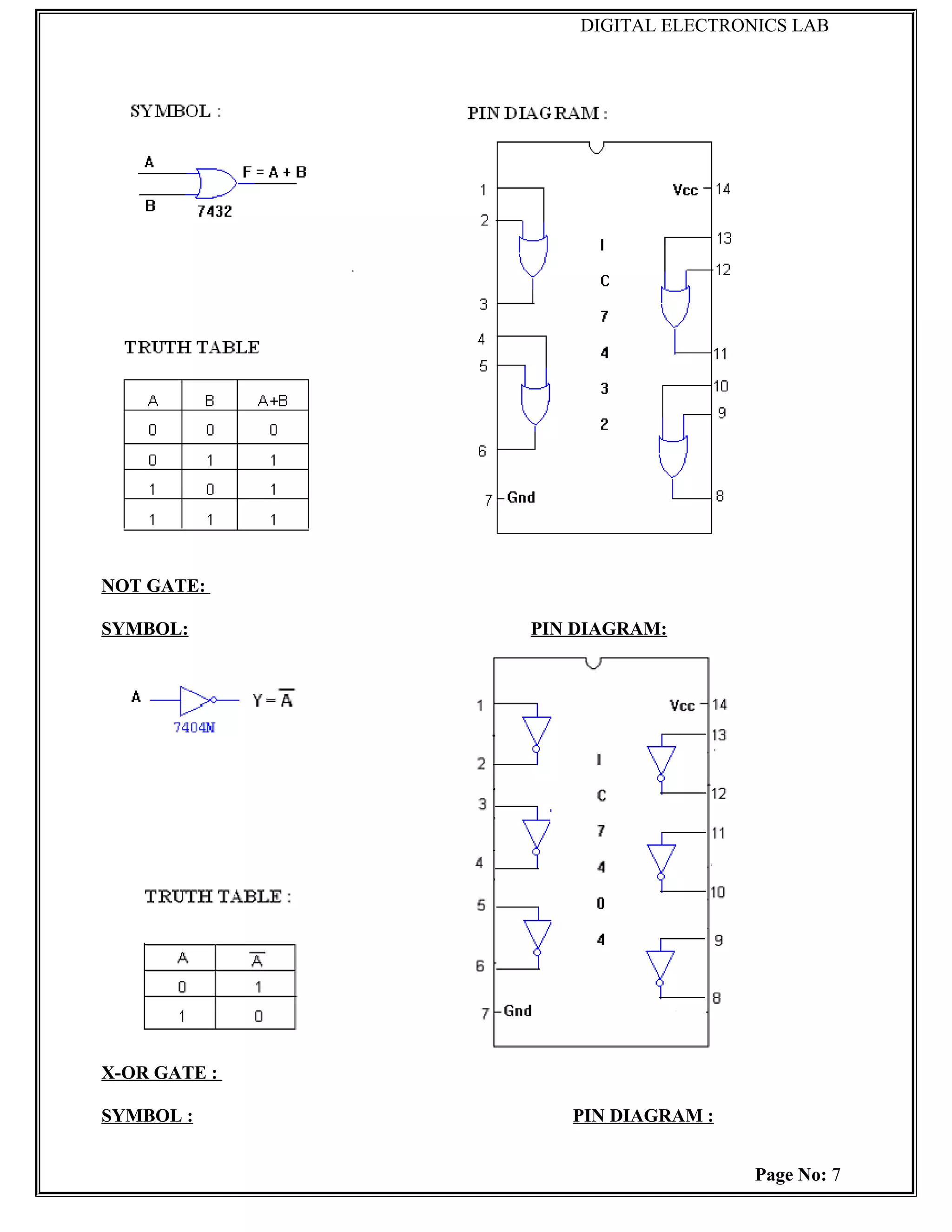
OR GATE:
The OR gate performs a logical addition commonly known as OR function.
The output is high when any one of the inputs is high. The output is low level when
both the inputs are low.
NOT GATE:
The NOT gate is called an inverter. The output is high when the input is
low. The output is low when the input is high.
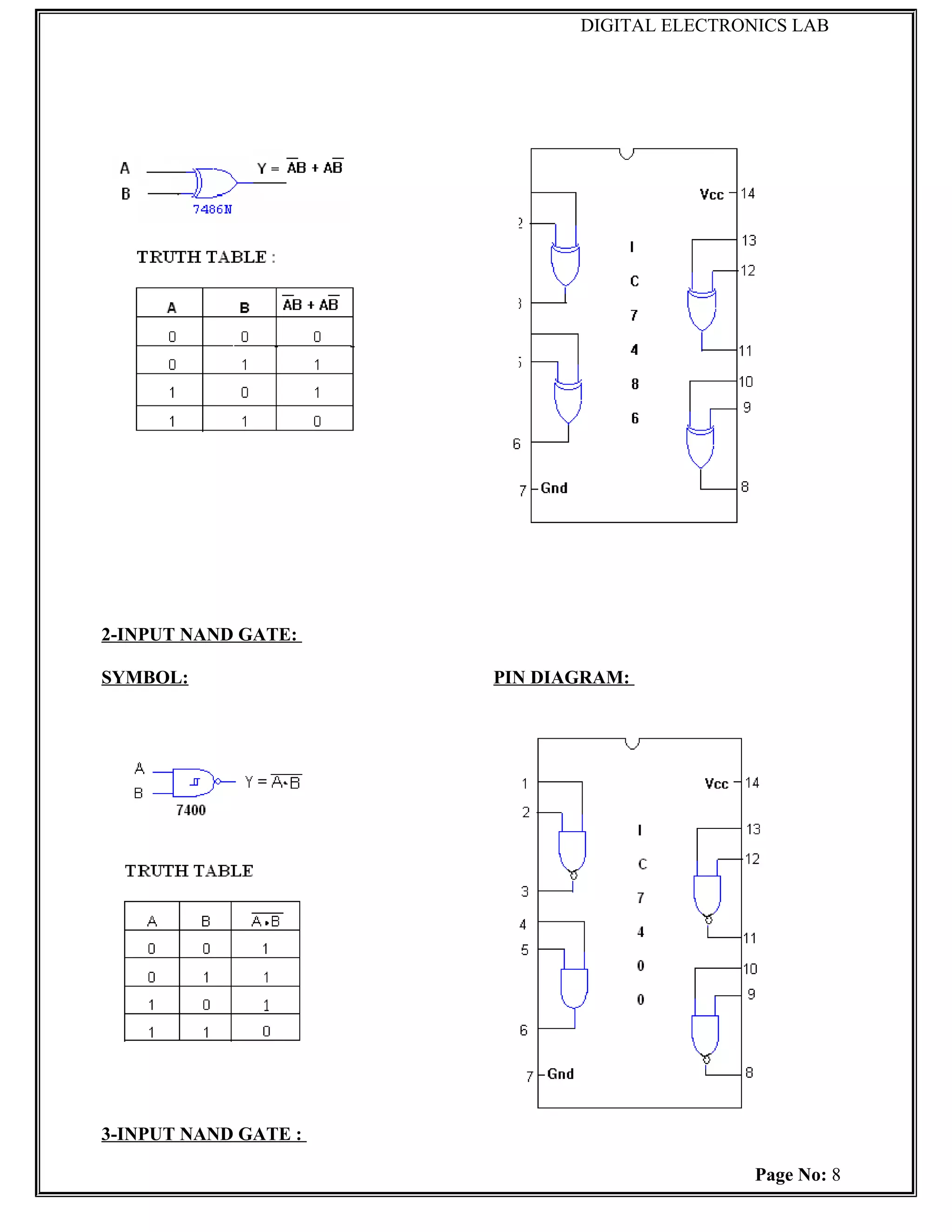
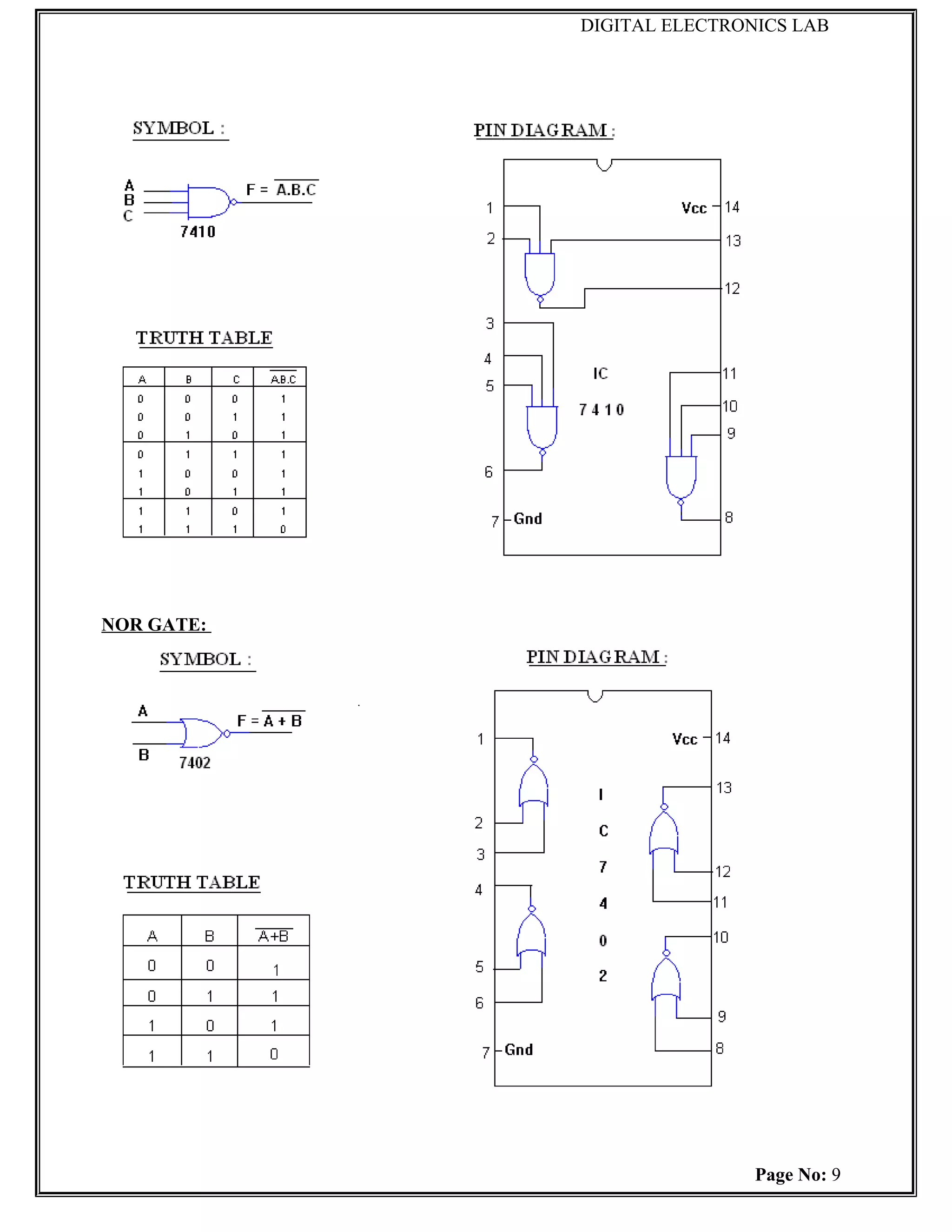
NAND GATE:
The NAND gate is a contraction of AND-NOT. The output is high when both
inputs are low and any one of the input is low .The output is low level when both
inputs are high.
NOR GATE:
The NOR gate is a contraction of OR-NOT. The output is high when both
inputs are low. The output is low when one or both inputs are high.
X-OR GATE:
The output is high when any one of the inputs is high. The output is low when
both the inputs are low and both the inputs are high.
Page No: 5
3.
DIGITAL ELECTRONICS LAB
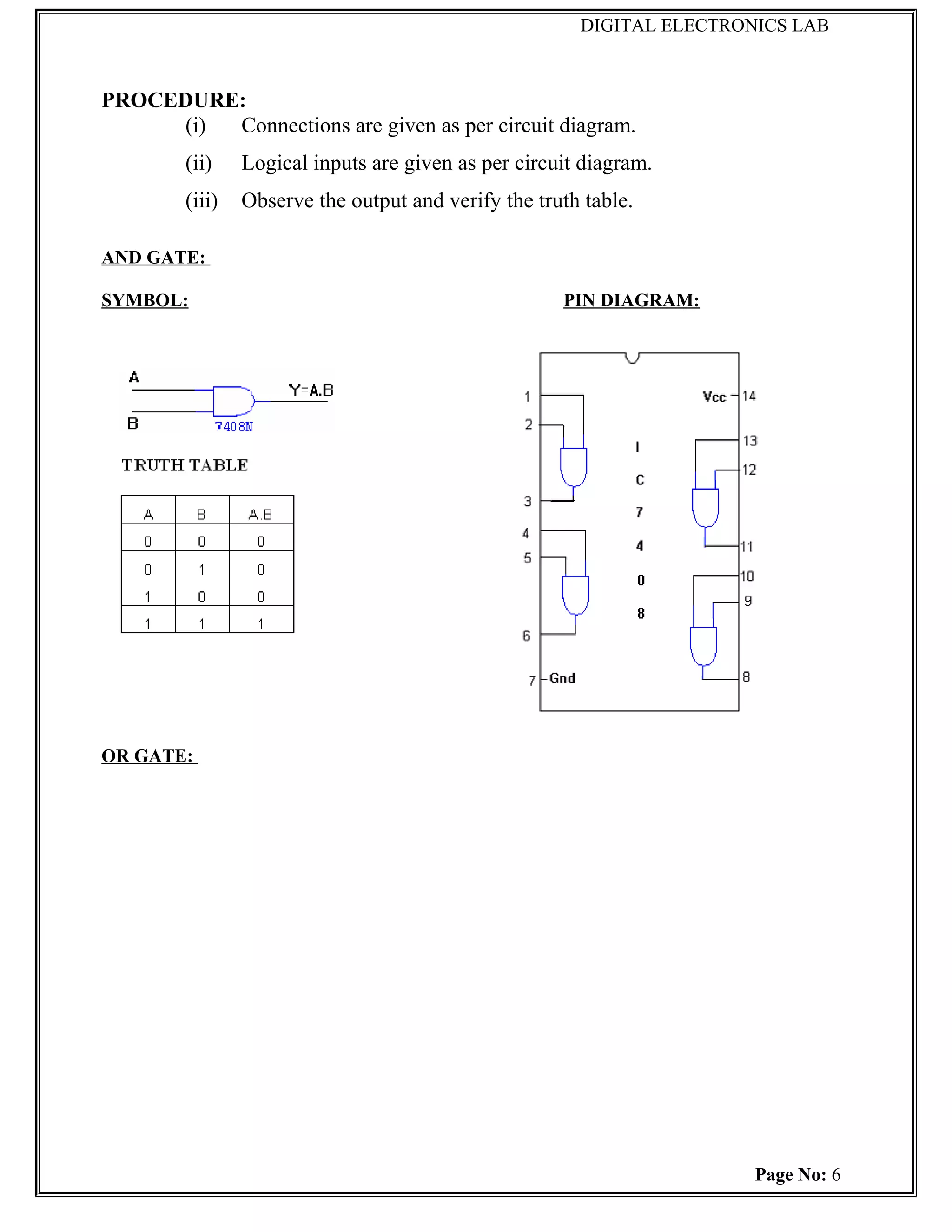
PROCEDURE:
(i) Connections are given as per circuit diagram.
(ii) Logical inputs are given as per circuit diagram.
(iii) Observe the output and verify the truth table.
AND GATE:
SYMBOL: PIN DIAGRAM:
OR GATE:
Page No: 6
DIGITAL ELECTRONICS LAB
RESULT:
Thus the logic gates are studied and their truth tables are verified.
Ex. No: 2
DESIGN OF ADDER AND SUBTRACTOR
Date:
AIM:
To design and construct half adder, full adder, half subtractor and full
subtractor circuits and verify the truth table using logic gates.
APPARATUS REQUIRED:
Sl.No. COMPONENT SPECIFICATION QTY.
1. AND GATE IC 7408 1
2. X-OR GATE IC 7486 1
3. NOT GATE IC 7404 1
4. OR GATE IC 7432 1
3. IC TRAINER KIT - 1
4. PATCH CORDS - 23
THEORY:
Page No: 10
8.
DIGITAL ELECTRONICS LAB
HALFADDER:
A half adder has two inputs for the two bits to be added and two outputs one
from the sum ‘ S’ and other from the carry ‘ c’ into the higher adder position. Above
circuit is called as a carry signal from the addition of the less significant bits sum
from the X-OR Gate the carry out from the AND gate.
FULL ADDER:
A full adder is a combinational circuit that forms the arithmetic sum of input; it
consists of three inputs and two outputs. A full adder is useful to add three bits at a
time but a half adder cannot do so. In full adder sum output will be taken from X-OR
Gate, carry output will be taken from OR Gate.
HALF SUBTRACTOR:
The half subtractor is constructed using X-OR and AND Gate. The half
subtractor has two input and two outputs. The outputs are difference and borrow. The
difference can be applied using X-OR Gate, borrow output can be implemented using
an AND Gate and an inverter.
FULL SUBTRACTOR:
The full subtractor is a combination of X-OR, AND, OR, NOT Gates. In a full
subtractor the logic circuit should have three inputs and two outputs. The two half
subtractor put together gives a full subtractor .The first half subtractor will be C and
A B. The output will be difference output of full subtractor. The expression AB
assembles the borrow output of the half subtractor and the second term is the inverted
difference output of first X-OR.
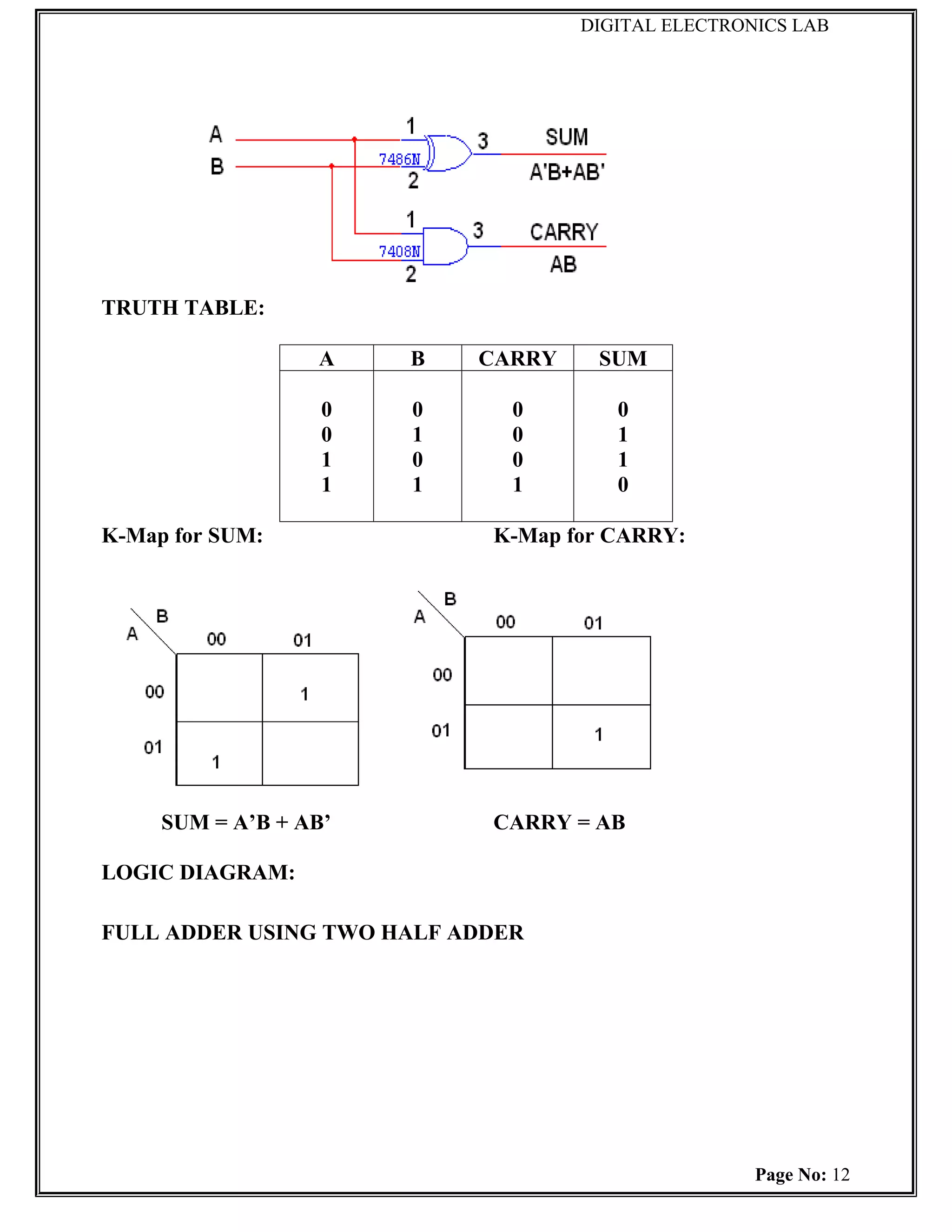
LOGIC DIAGRAM:
HALF ADDER
Page No: 11
9.
DIGITAL ELECTRONICS LAB
TRUTHTABLE:
A B CARRY SUM
0 0 0 0
0 1 0 1
1 0 0 1
1 1 1 0
K-Map for SUM: K-Map for CARRY:
SUM = A’B + AB’ CARRY = AB
LOGIC DIAGRAM:
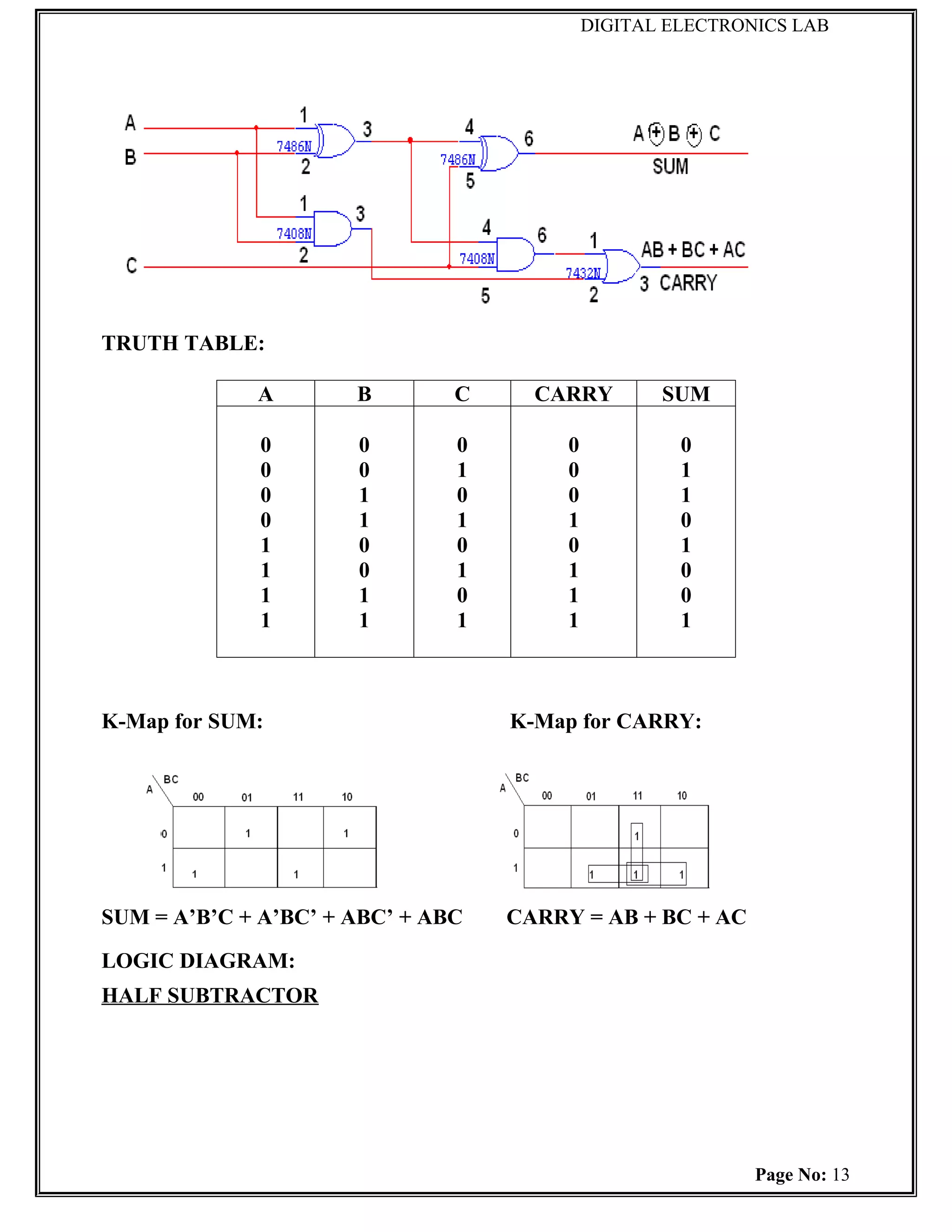
FULL ADDER USING TWO HALF ADDER
Page No: 12
10.
DIGITAL ELECTRONICS LAB
TRUTHTABLE:
A B C CARRY SUM
0 0 0 0 0
0 0 1 0 1
0 1 0 0 1
0 1 1 1 0
1 0 0 0 1
1 0 1 1 0
1 1 0 1 0
1 1 1 1 1
K-Map for SUM: K-Map for CARRY:
SUM = A’B’C + A’BC’ + ABC’ + ABC CARRY = AB + BC + AC
LOGIC DIAGRAM:
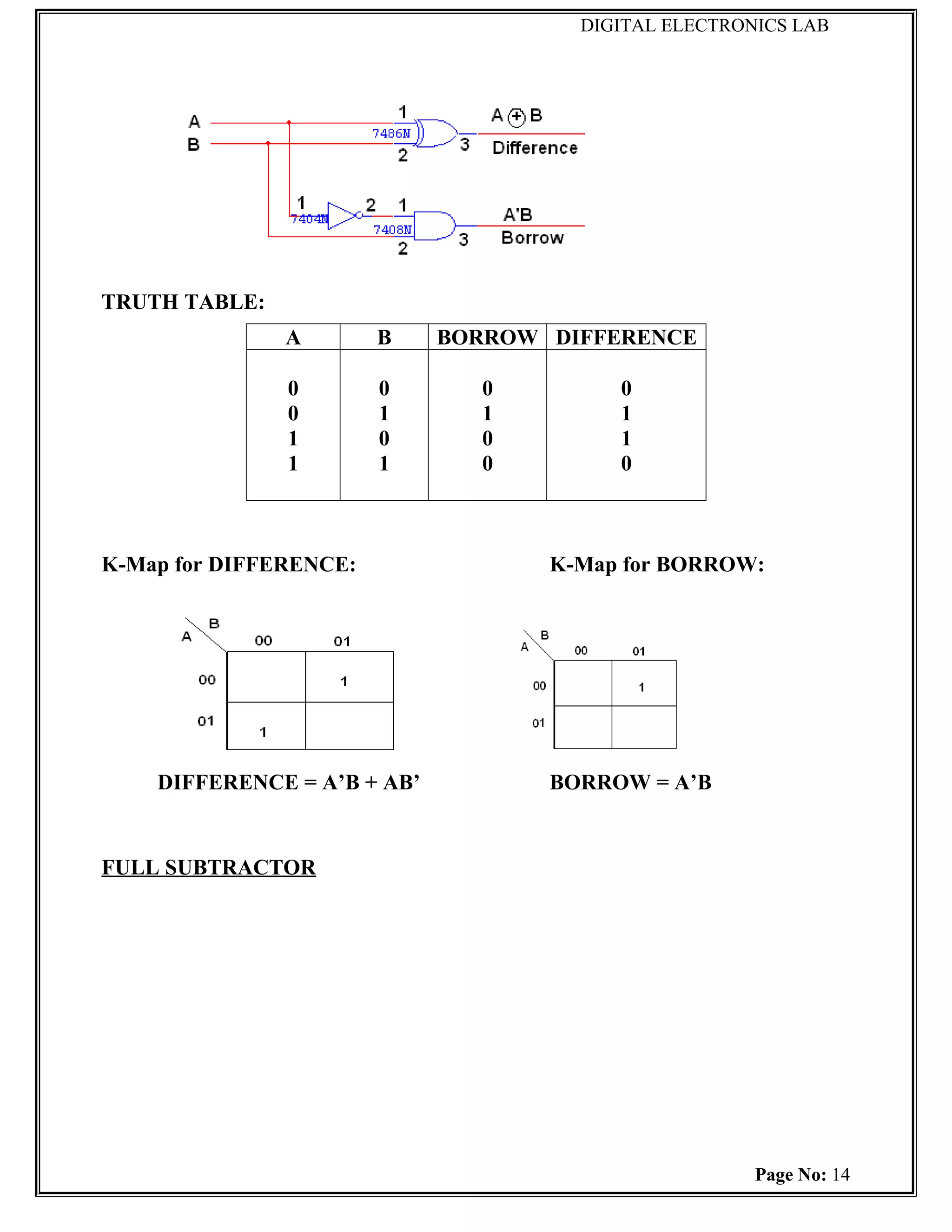
HALF SUBTRACTOR
Page No: 13
11.
DIGITAL ELECTRONICS LAB
TRUTHTABLE:
A B BORROW DIFFERENCE
0 0 0 0
0 1 1 1
1 0 0 1
1 1 0 0
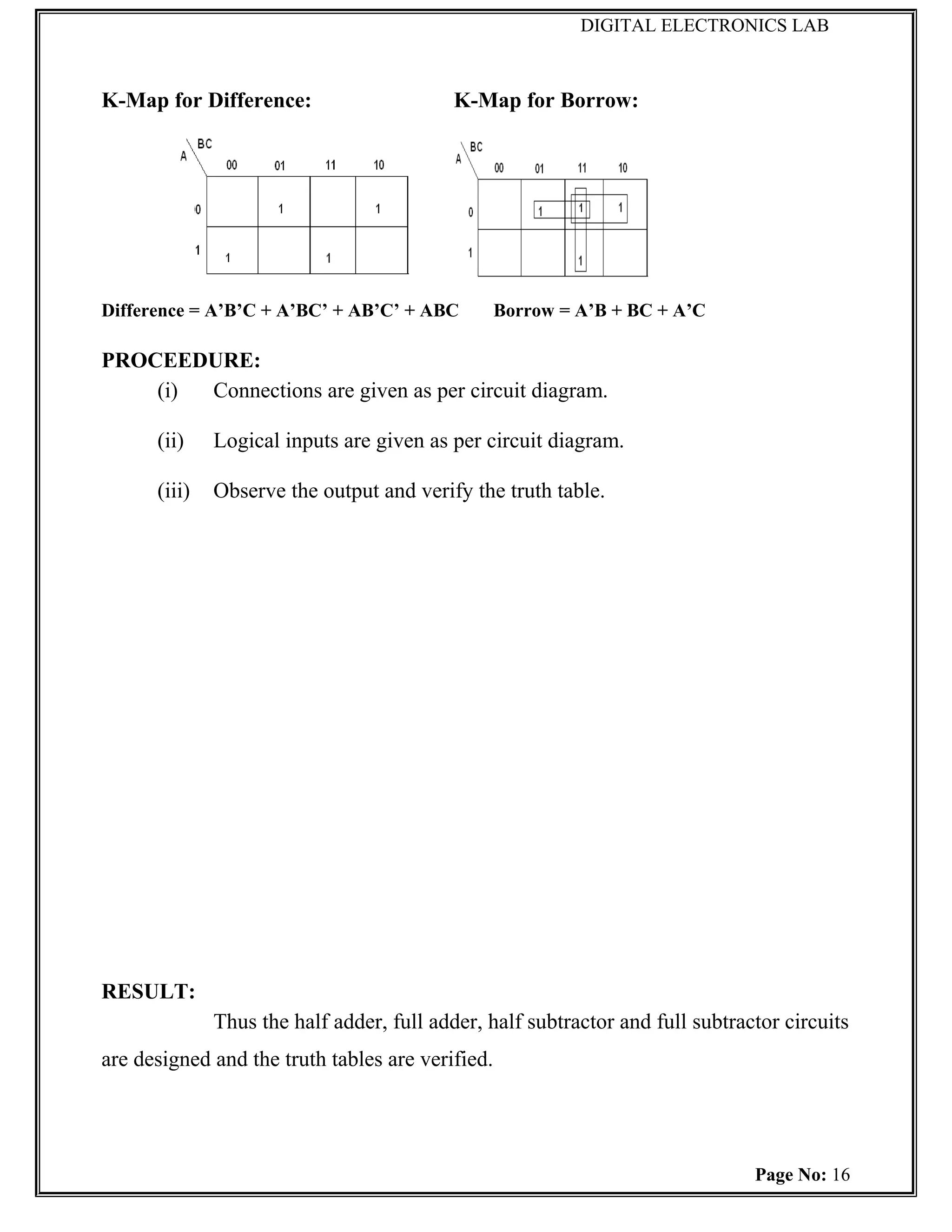
K-Map for DIFFERENCE: K-Map for BORROW:
DIFFERENCE = A’B + AB’ BORROW = A’B
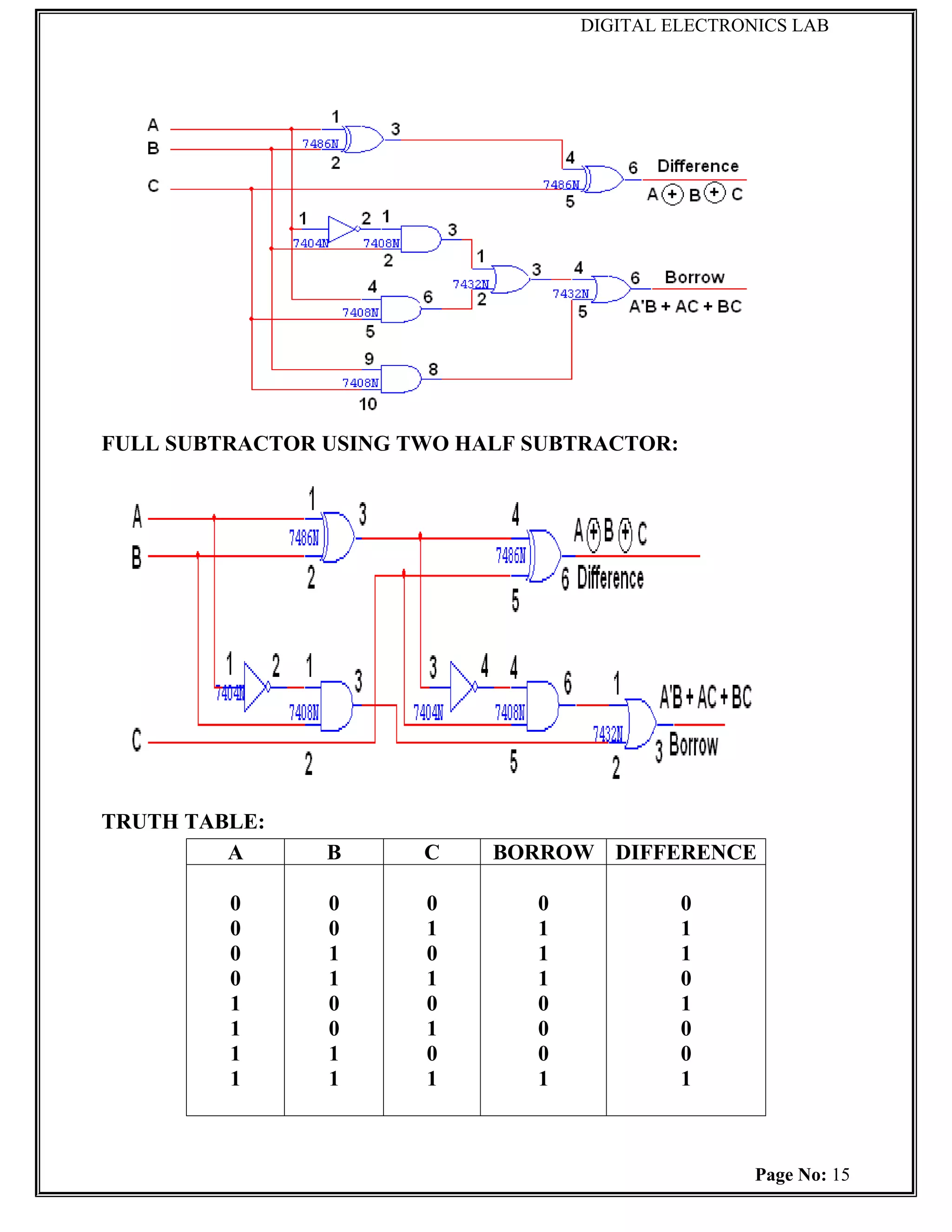
FULL SUBTRACTOR
Page No: 14
12.
DIGITAL ELECTRONICS LAB
FULLSUBTRACTOR USING TWO HALF SUBTRACTOR:
TRUTH TABLE:
A B C BORROW DIFFERENCE
0 0 0 0 0
0 0 1 1 1
0 1 0 1 1
0 1 1 1 0
1 0 0 0 1
1 0 1 0 0
1 1 0 0 0
1 1 1 1 1
Page No: 15
13.
DIGITAL ELECTRONICS LAB
K-Mapfor Difference: K-Map for Borrow:
Difference = A’B’C + A’BC’ + AB’C’ + ABC Borrow = A’B + BC + A’C
PROCEEDURE:
(i) Connections are given as per circuit diagram.
(ii) Logical inputs are given as per circuit diagram.
(iii) Observe the output and verify the truth table.
RESULT:
Thus the half adder, full adder, half subtractor and full subtractor circuits
are designed and the truth tables are verified.
Page No: 16
14.
DIGITAL ELECTRONICS LAB
Ex.No: 3
DESIGN AND IMPLEMENTATION OF CODE CONVERTOR
Date:
AIM:
To design and implement 4-bit
(i) Binary to gray code converter
(ii) Gray to binary code converter
(iii) BCD to excess-3 code converter
(iv) Excess-3 to BCD code converter
APPARATUS REQUIRED:
Sl.No. COMPONENT SPECIFICATION QTY.
1. X-OR GATE IC 7486 1
2. AND GATE IC 7408 1
3. OR GATE IC 7432 1
4. NOT GATE IC 7404 1
5. IC TRAINER KIT - 1
6. PATCH CORDS - 35
THEORY:
The availability of large variety of codes for the same discrete elements of
information results in the use of different codes by different systems. A conversion
circuit must be inserted between the two systems if each uses different codes for
same information. Thus, code converter is a circuit that makes the two systems
compatible even though each uses different binary code.
A code converter is a circuit that makes the two systems compatible even
though each uses a different binary code. To convert from binary code to Excess-3
code, the input lines must supply the bit combination of elements as specified by
code and the output lines generate the corresponding bit combination of code. Each
one of the four maps represents one of the four outputs of the circuit as a function of
the four input variables.
Page No: 17
15.
DIGITAL ELECTRONICS LAB
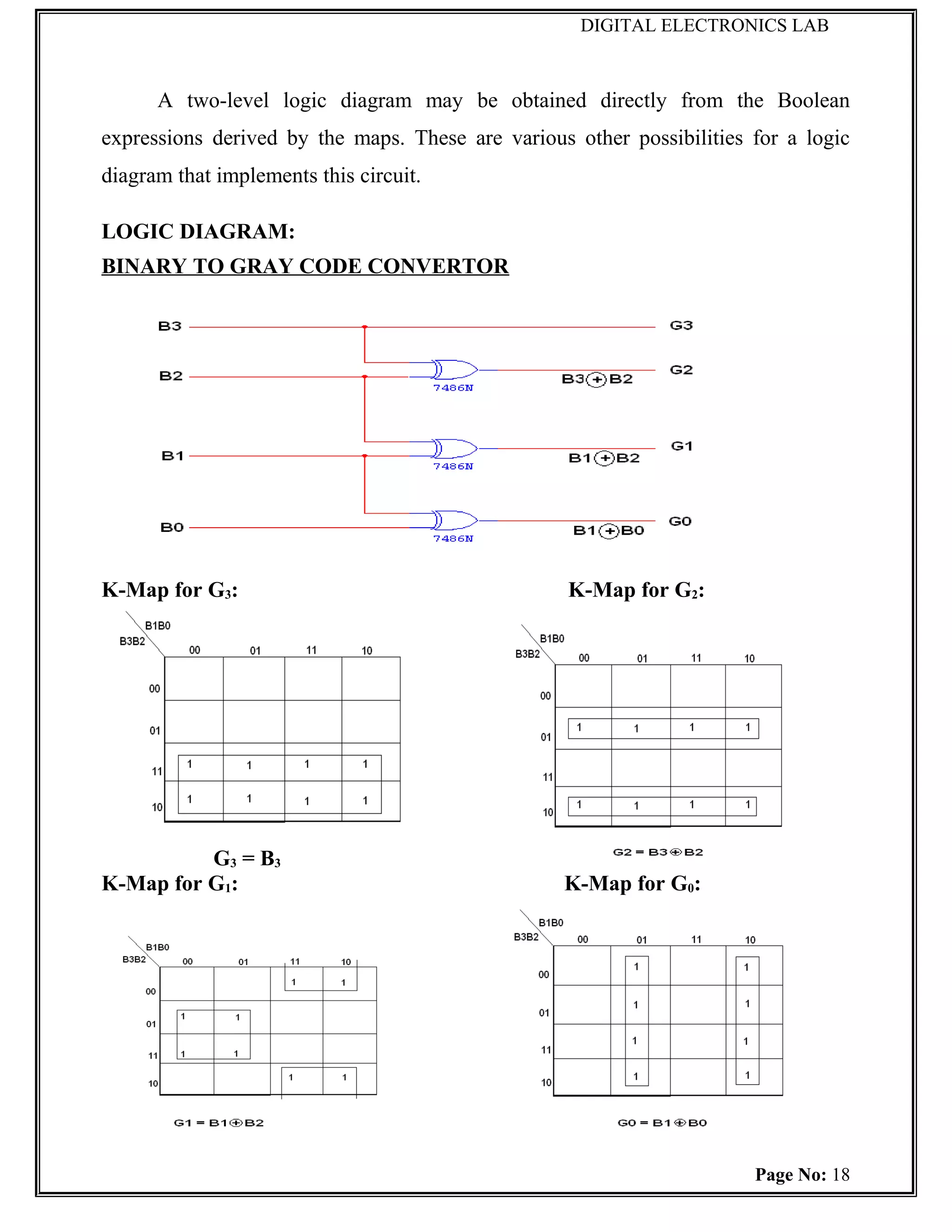
A two-level logic diagram may be obtained directly from the Boolean
expressions derived by the maps. These are various other possibilities for a logic
diagram that implements this circuit.
LOGIC DIAGRAM:
BINARY TO GRAY CODE CONVERTOR
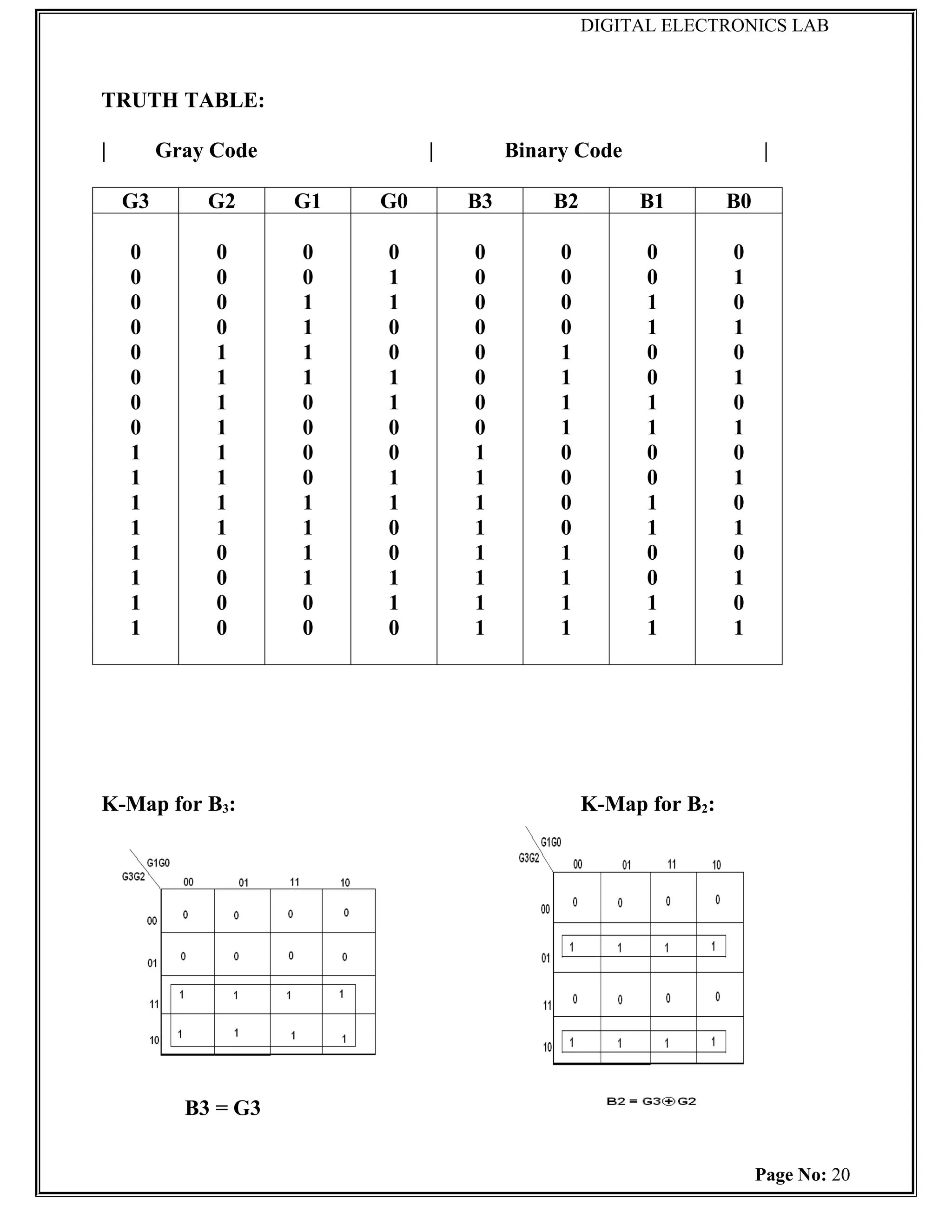
K-Map for G3: K-Map for G2:
G3 = B3
K-Map for G1: K-Map for G0:
Page No: 18
DIGITAL ELECTRONICS LAB
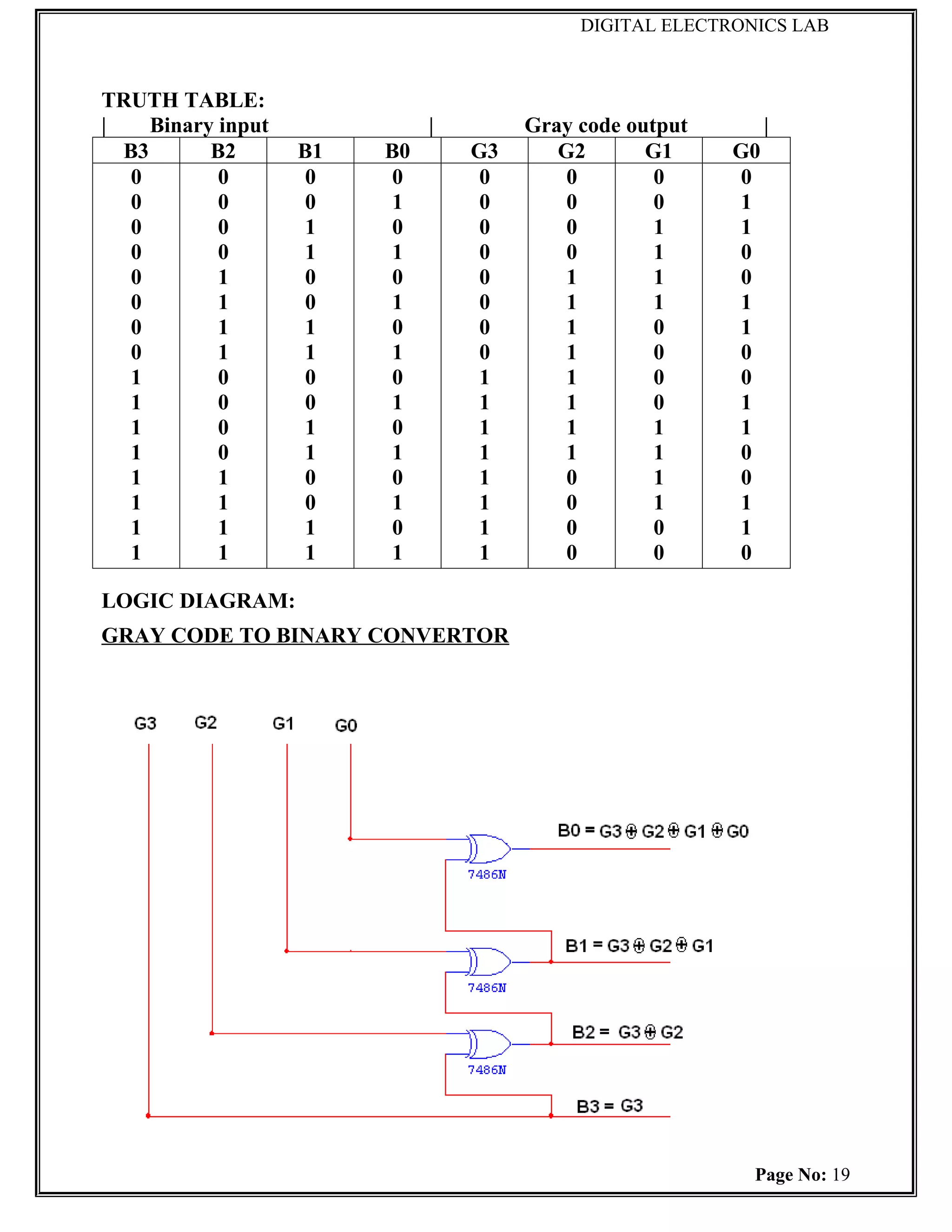
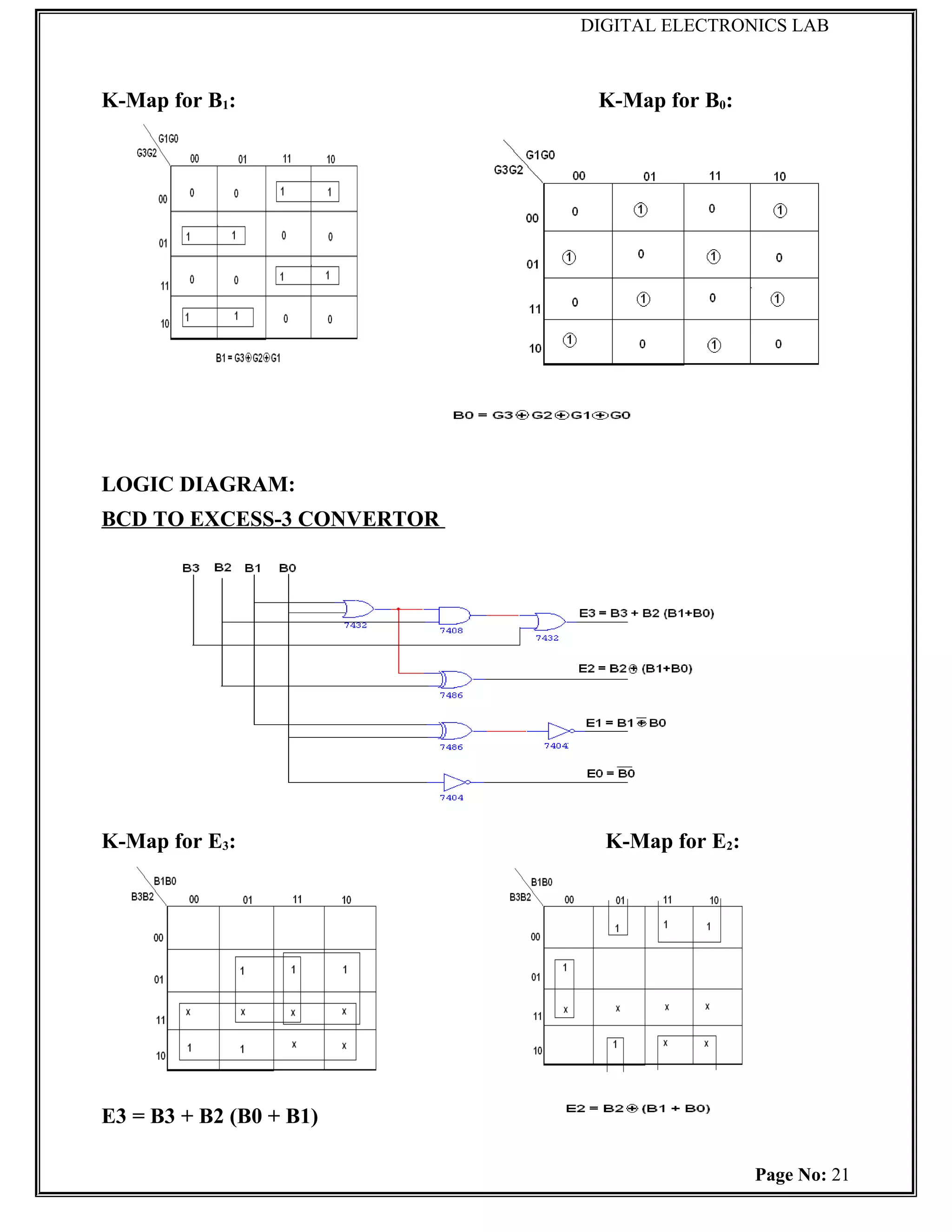
K-Mapfor B1: K-Map for B0:
LOGIC DIAGRAM:
BCD TO EXCESS-3 CONVERTOR
K-Map for E3: K-Map for E2:
E3 = B3 + B2 (B0 + B1)
Page No: 21
19.
DIGITAL ELECTRONICS LAB
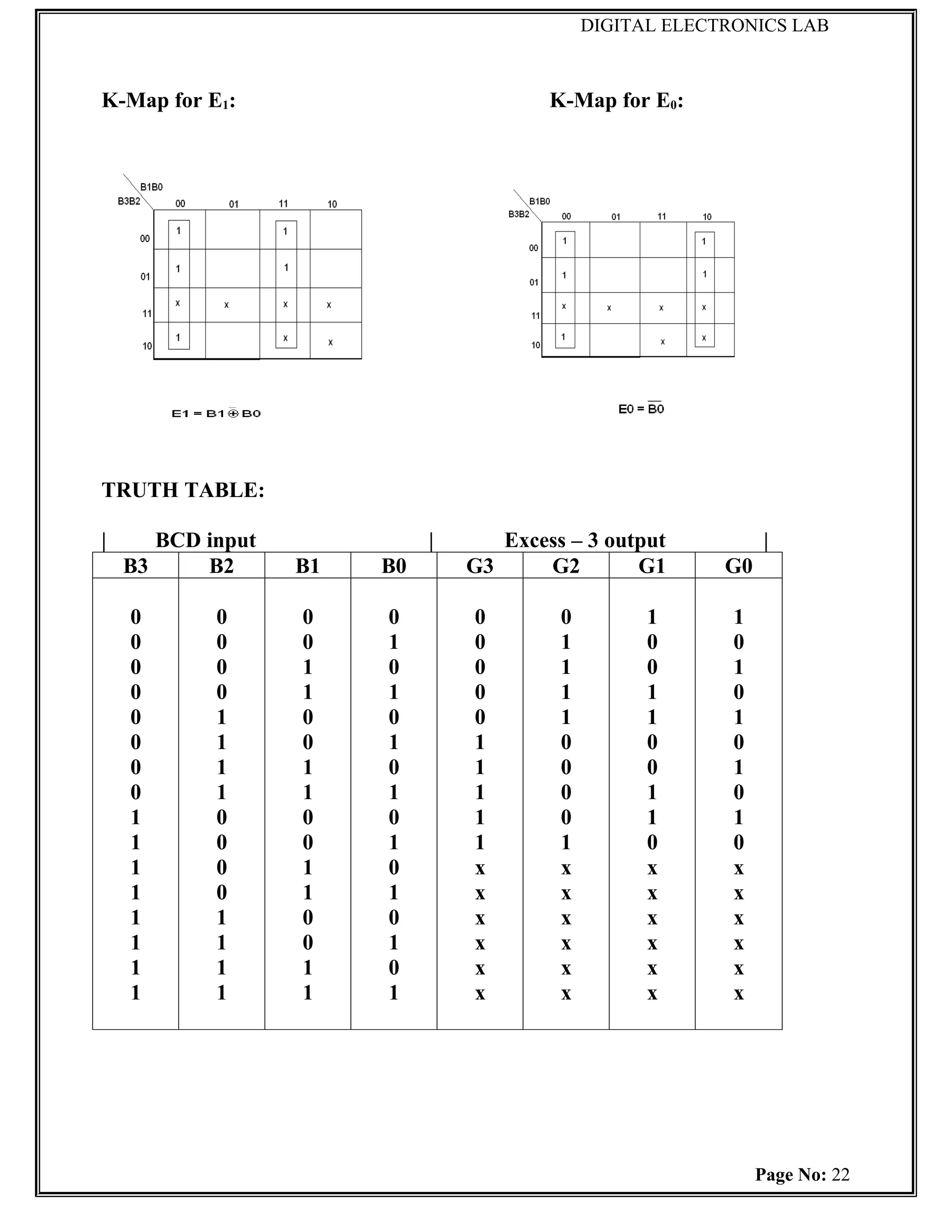
K-Mapfor E1: K-Map for E0:
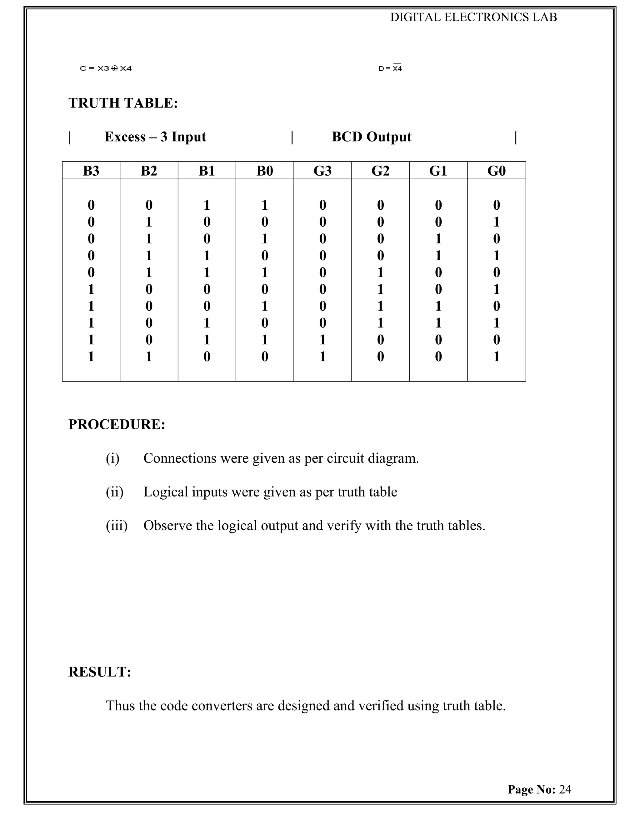
TRUTH TABLE:
| BCD input | Excess – 3 output |
B3 B2 B1 B0 G3 G2 G1 G0
0 0 0 0 0 0 1 1
0 0 0 1 0 1 0 0
0 0 1 0 0 1 0 1
0 0 1 1 0 1 1 0
0 1 0 0 0 1 1 1
0 1 0 1 1 0 0 0
0 1 1 0 1 0 0 1
0 1 1 1 1 0 1 0
1 0 0 0 1 0 1 1
1 0 0 1 1 1 0 0
1 0 1 0 x x x x
1 0 1 1 x x x x
1 1 0 0 x x x x
1 1 0 1 x x x x
1 1 1 0 x x x x
1 1 1 1 x x x x
Page No: 22
20.
DIGITAL ELECTRONICS LAB
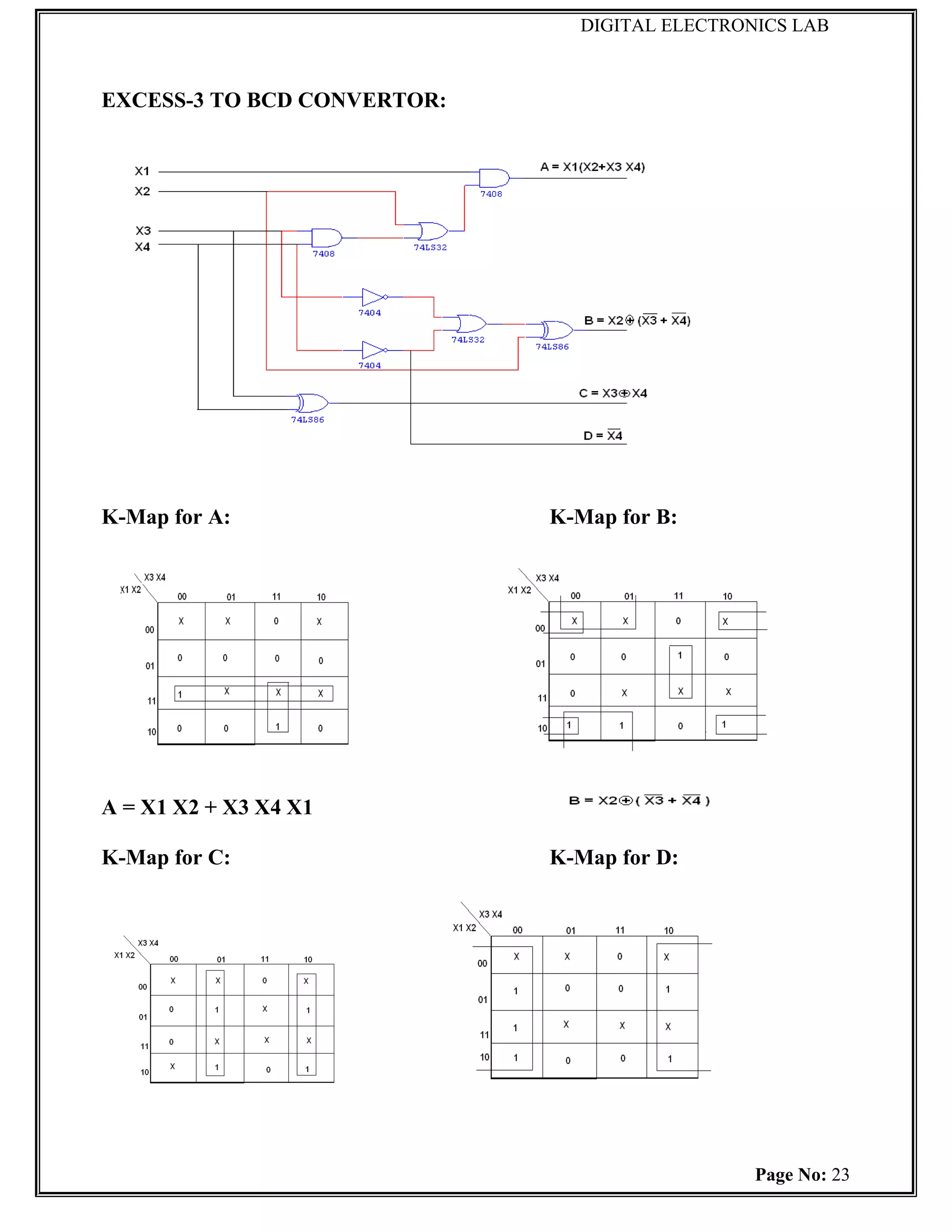
EXCESS-3TO BCD CONVERTOR:
K-Map for A: K-Map for B:
A = X1 X2 + X3 X4 X1
K-Map for C: K-Map for D:
Page No: 23
21.
DIGITAL ELECTRONICS LAB
TRUTHTABLE:
| Excess – 3 Input | BCD Output |
B3 B2 B1 B0 G3 G2 G1 G0
0 0 1 1 0 0 0 0
0 1 0 0 0 0 0 1
0 1 0 1 0 0 1 0
0 1 1 0 0 0 1 1
0 1 1 1 0 1 0 0
1 0 0 0 0 1 0 1
1 0 0 1 0 1 1 0
1 0 1 0 0 1 1 1
1 0 1 1 1 0 0 0
1 1 0 0 1 0 0 1
PROCEDURE:
(i) Connections were given as per circuit diagram.
(ii) Logical inputs were given as per truth table
(iii) Observe the logical output and verify with the truth tables.
RESULT:
Thus the code converters are designed and verified using truth table.
Page No: 24
22.
DIGITAL ELECTRONICS LAB
Ex.No: 4
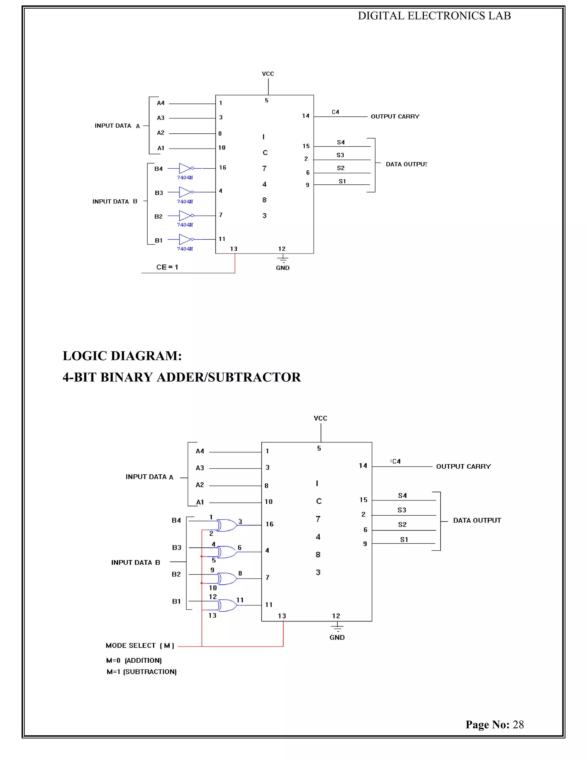
DESIGN OF 4-BIT ADDER AND SUBTRACTOR
Date:
AIM:
To design and implement 4-bit adder and subtractor using IC 7483.
APPARATUS REQUIRED:
Sl.No. COMPONENT SPECIFICATION QTY.
1. IC IC 7483 1
2. EX-OR GATE IC 7486 1
3. NOT GATE IC 7404 1
3. IC TRAINER KIT - 1
4. PATCH CORDS - 40
THEORY:
4 BIT BINARY ADDER:
A binary adder is a digital circuit that produces the arithmetic sum of two
binary numbers. It can be constructed with full adders connected in cascade, with the
output carry from each full adder connected to the input carry of next full adder in
chain. The augends bits of ‘A’ and the addend bits of ‘B’ are designated by subscript
numbers from right to left, with subscript 0 denoting the least significant bits. The
carries are connected in chain through the full adder. The input carry to the adder is
C0 and it ripples through the full adder to the output carry C4.
4 BIT BINARY SUBTRACTOR:
The circuit for subtracting A-B consists of an adder with inverters, placed
between each data input ‘B’ and the corresponding input of full adder. The input
carry C0 must be equal to 1 when performing subtraction.
Page No: 25
23.
DIGITAL ELECTRONICS LAB
4BIT BINARY ADDER/SUBTRACTOR:
The addition and subtraction operation can be combined into one circuit with
one common binary adder. The mode input M controls the operation. When M=0, the
circuit is adder circuit. When M=1, it becomes subtractor.
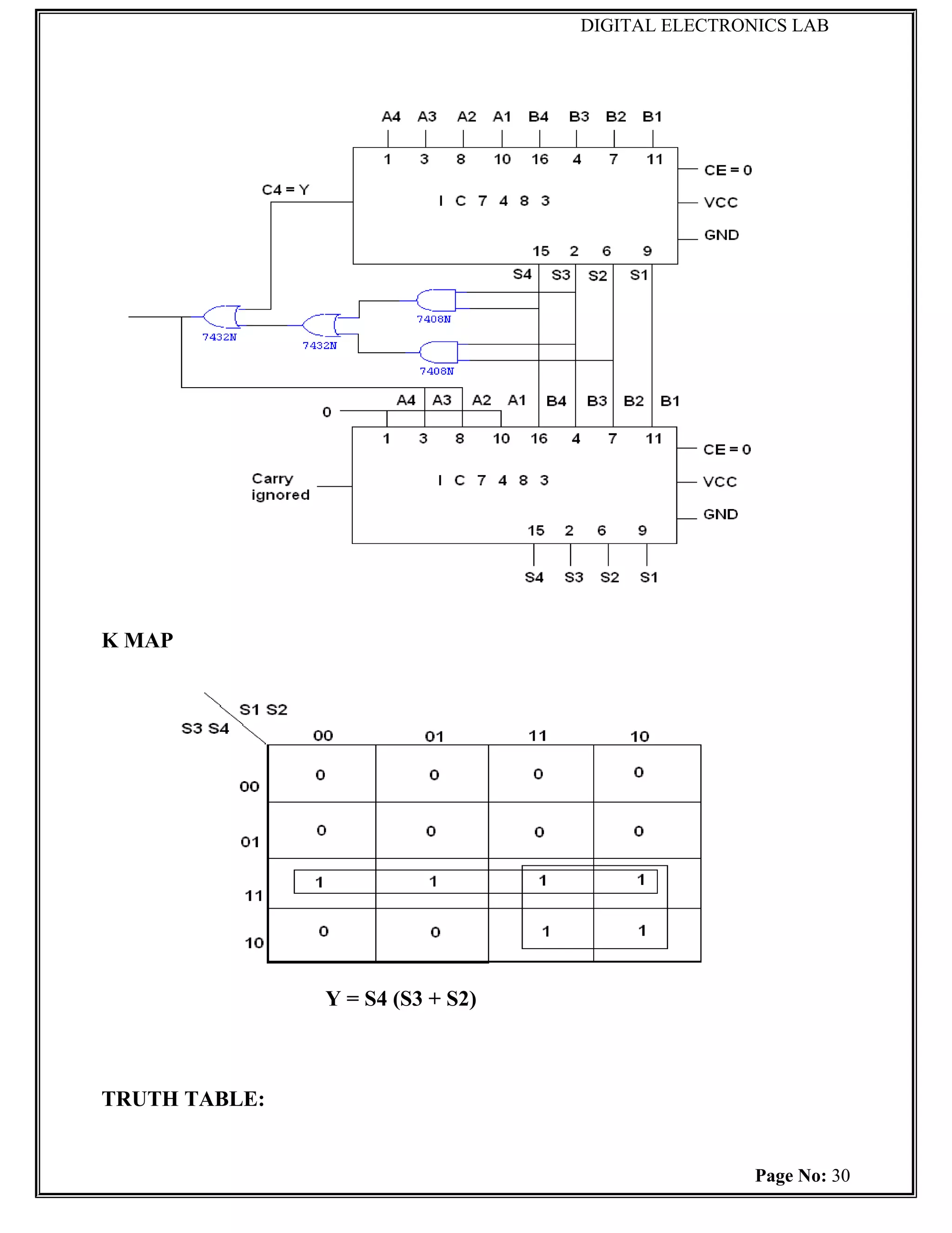
4 BIT BCD ADDER:
Consider the arithmetic addition of two decimal digits in BCD, together with
an input carry from a previous stage. Since each input digit does not exceed 9, the
output sum cannot be greater than 19, the 1 in the sum being an input carry. The
output of two decimal digits must be represented in BCD and should appear in the
form listed in the columns.
ABCD adder that adds 2 BCD digits and produce a sum digit in BCD. The 2
decimal digits, together with the input carry, are first added in the top 4 bit adder to
produce the binary sum.
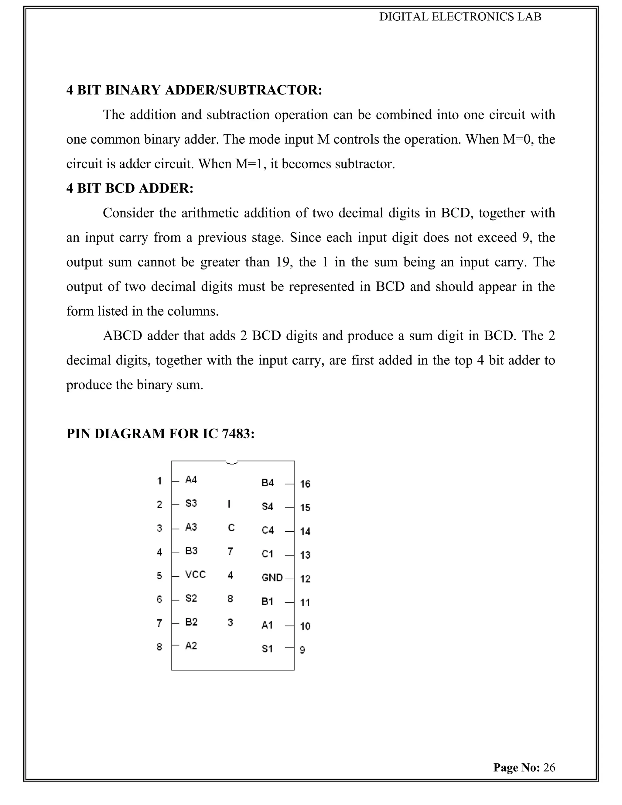
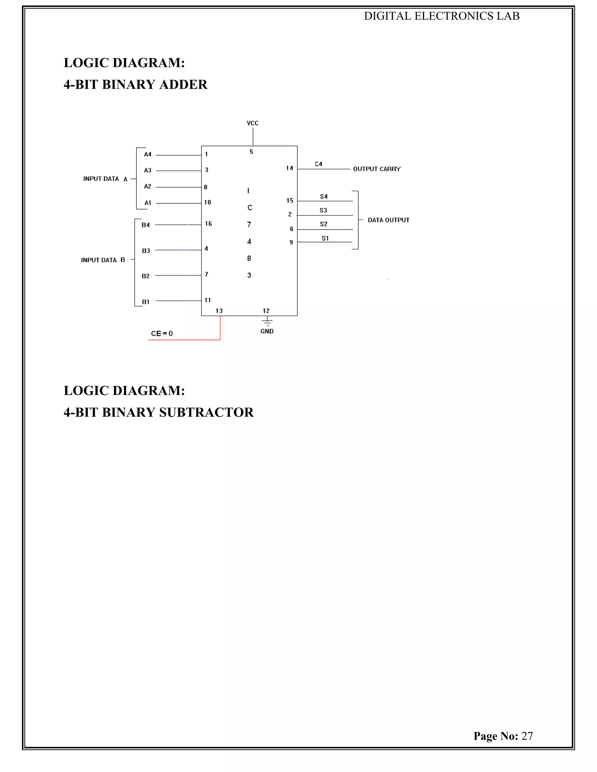
PIN DIAGRAM FOR IC 7483:
Page No: 26
DIGITAL ELECTRONICS LAB
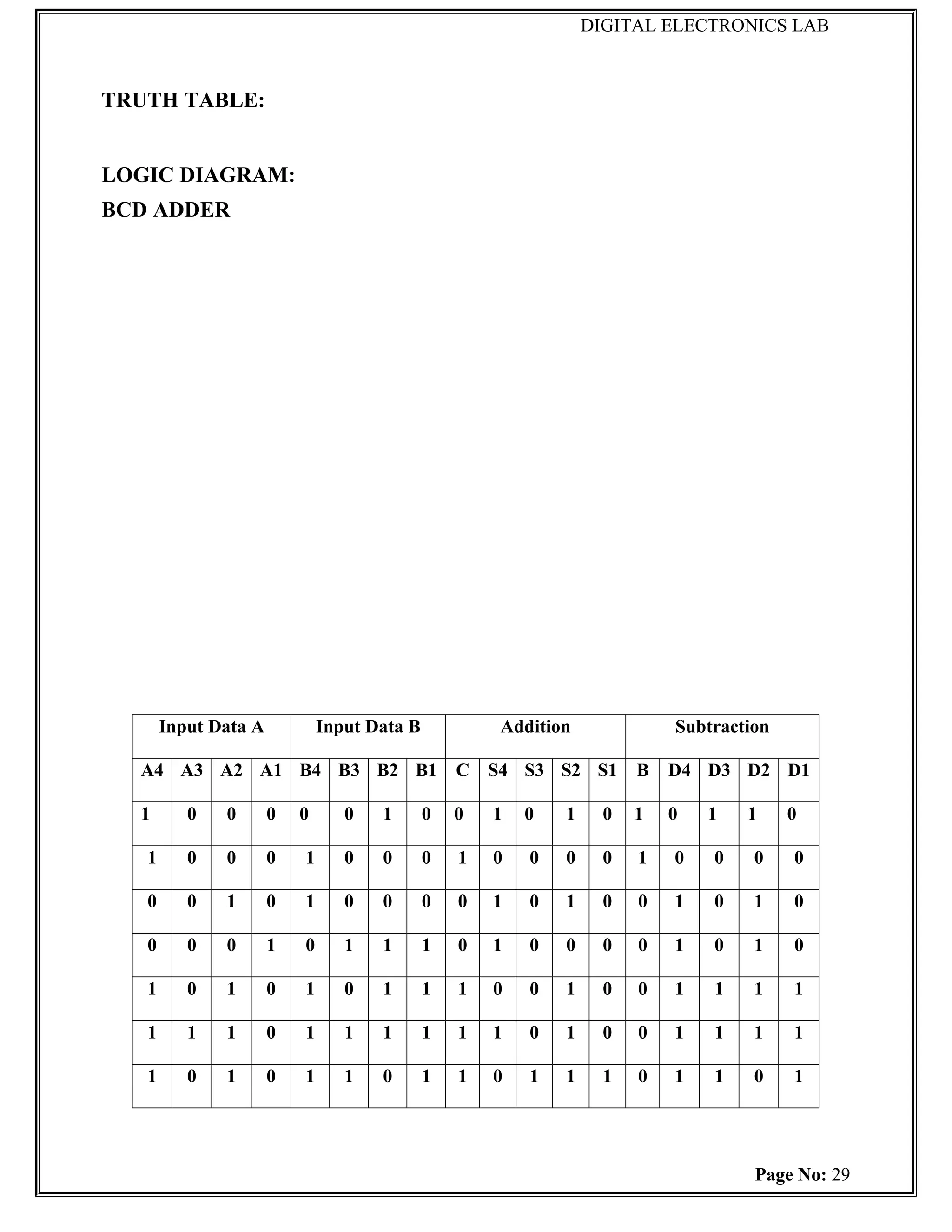
BCD SUM CARRY
S4 S3 S2 S1 C
0 0 0 0 0
0 0 0 1 0
0 0 1 0 0
0 0 1 1 0
0 1 0 0 0
0 1 0 1 0
0 1 1 0 0
0 1 1 1 0
1 0 0 0 0
1 0 0 1 0
1 0 1 0 1
1 0 1 1 1
1 1 0 0 1
1 1 0 1 1
1 1 1 0 1
1 1 1 1 1
PROCEDURE:
(i) Connections were given as per circuit diagram.
(ii) Logical inputs were given as per truth table
(iii) Observe the logical output and verify with the truth tables.
RESULT:
Thus the 4-bit adder and subtractor circuits are implemented using IC 7483.
Ex. No: 5
Page No: 31
29.
DIGITAL ELECTRONICS LAB
Date:
DESIGN AND IMPLEMENTATION OF MAGNITUDE
COMPARATOR
AIM:
To design and implement
(i) 2 – Bit magnitude comparator using basic gates.
(ii) 8 – Bit magnitude comparator using IC 7485.
APPARATUS REQUIRED:
Sl.No. COMPONENT SPECIFICATION QTY.
1. AND GATE IC 7408 2
2. X-OR GATE IC 7486 1
3. OR GATE IC 7432 1
4. NOT GATE IC 7404 1
5. 4-BIT MAGNITUDE IC 7485 2
COMPARATOR
6. IC TRAINER KIT - 1
7. PATCH CORDS - 30
THEORY:
The comparison of two numbers is an operator that determine one number is
greater than, less than (or) equal to the other number. A magnitude comparator is a
combinational circuit that compares two numbers A and B and determine their
relative magnitude. The outcome of the comparator is specified by three binary
variables that indicate whether A>B, A=B (or) A<B.
A = A3 A2 A1 A0 B = B3 B2 B1 B0
The equality of the two numbers and B is displayed in a combinational circuit
designated by the symbol (A=B).
This indicates A greater than B, then inspect the relative magnitude of pairs of
significant digits starting from most significant position. A is 0 and that of B is 0.
We have A<B, the sequential comparison can be expanded as
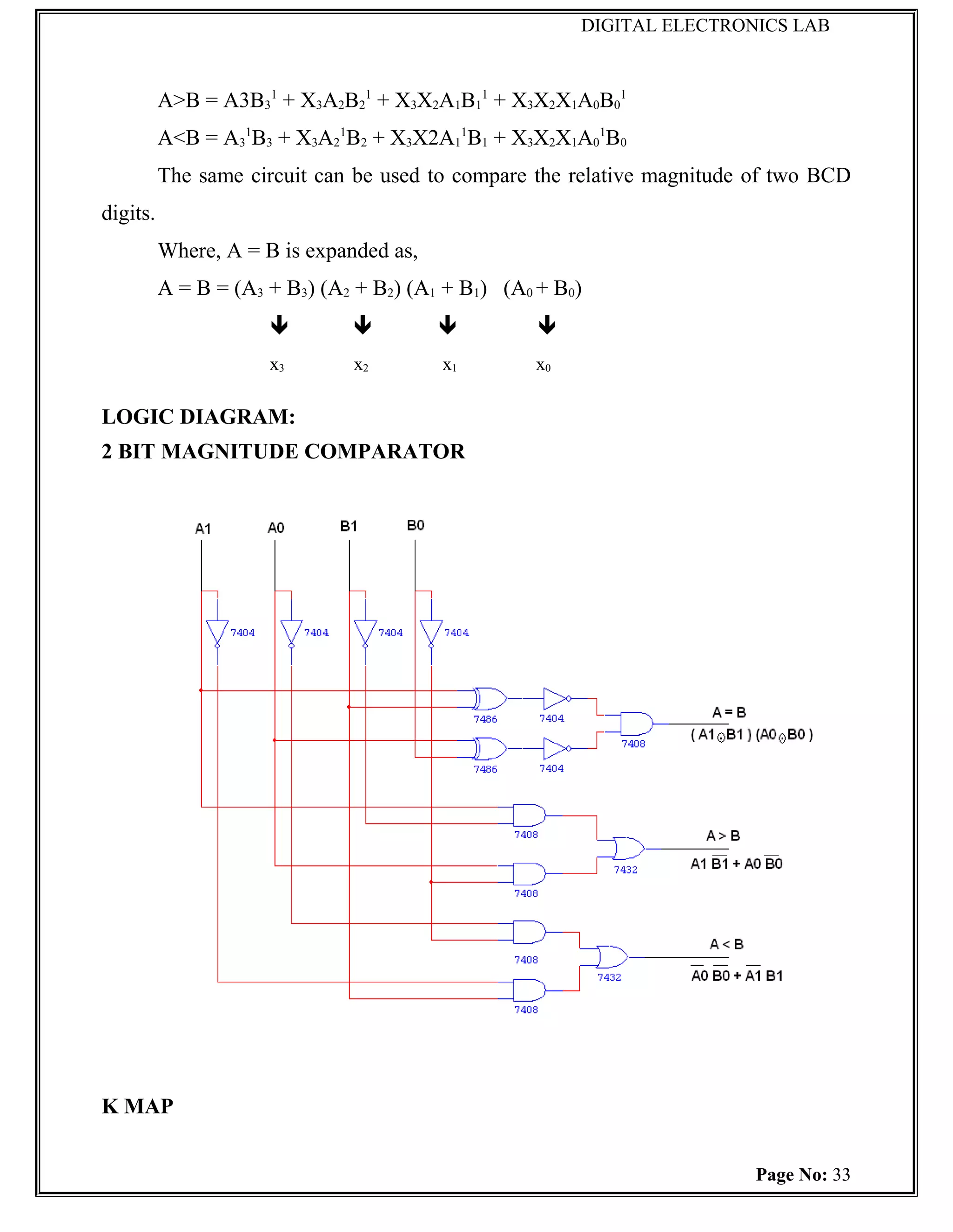
Page No: 32
30.
DIGITAL ELECTRONICS LAB
A>B = A3B31 + X3A2B21 + X3X2A1B11 + X3X2X1A0B01
A<B = A31B3 + X3A21B2 + X3X2A11B1 + X3X2X1A01B0
The same circuit can be used to compare the relative magnitude of two BCD
digits.
Where, A = B is expanded as,
A = B = (A3 + B3) (A2 + B2) (A1 + B1) (A0 + B0)
x3 x2 x1 x0
LOGIC DIAGRAM:
2 BIT MAGNITUDE COMPARATOR
K MAP
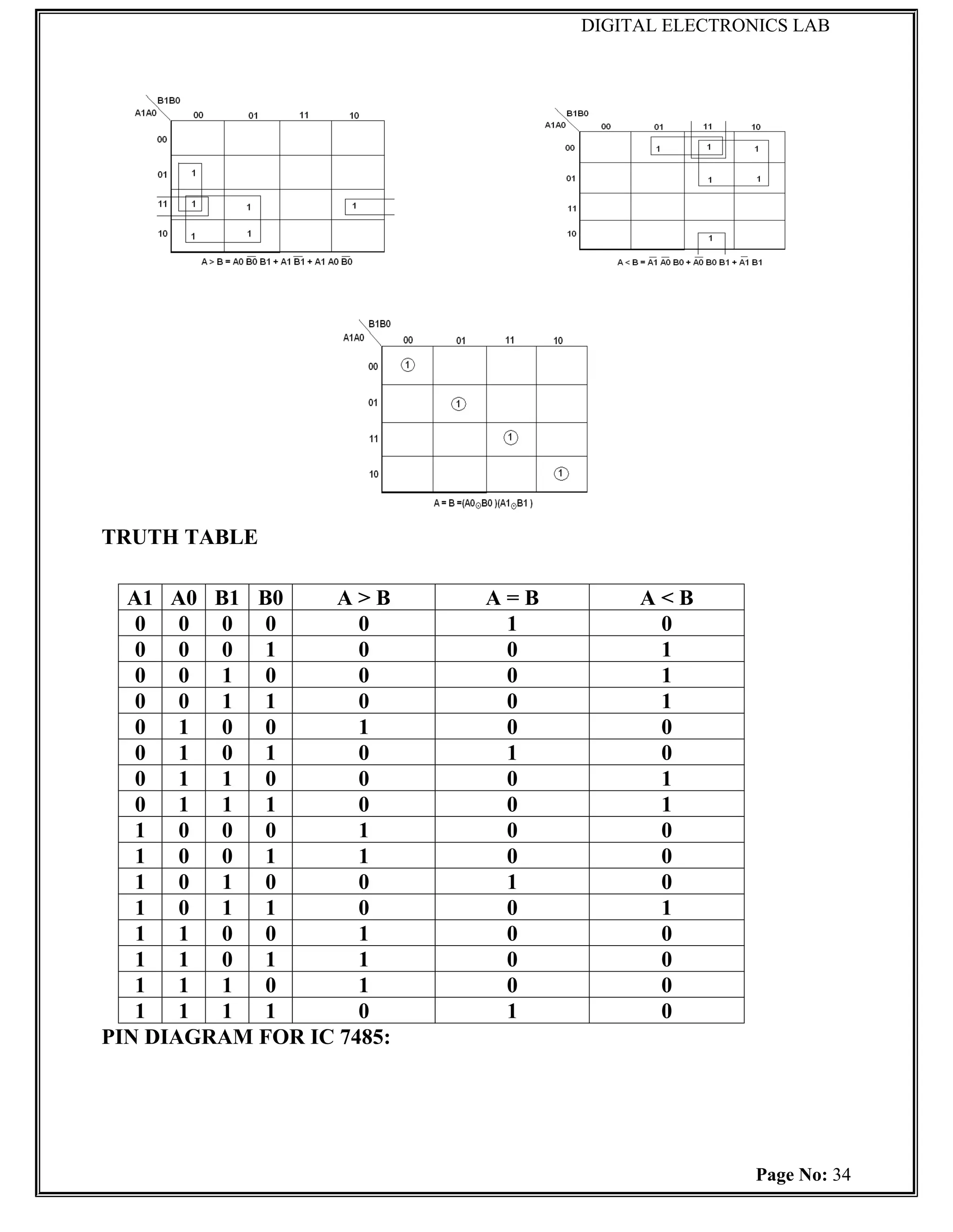
Page No: 33
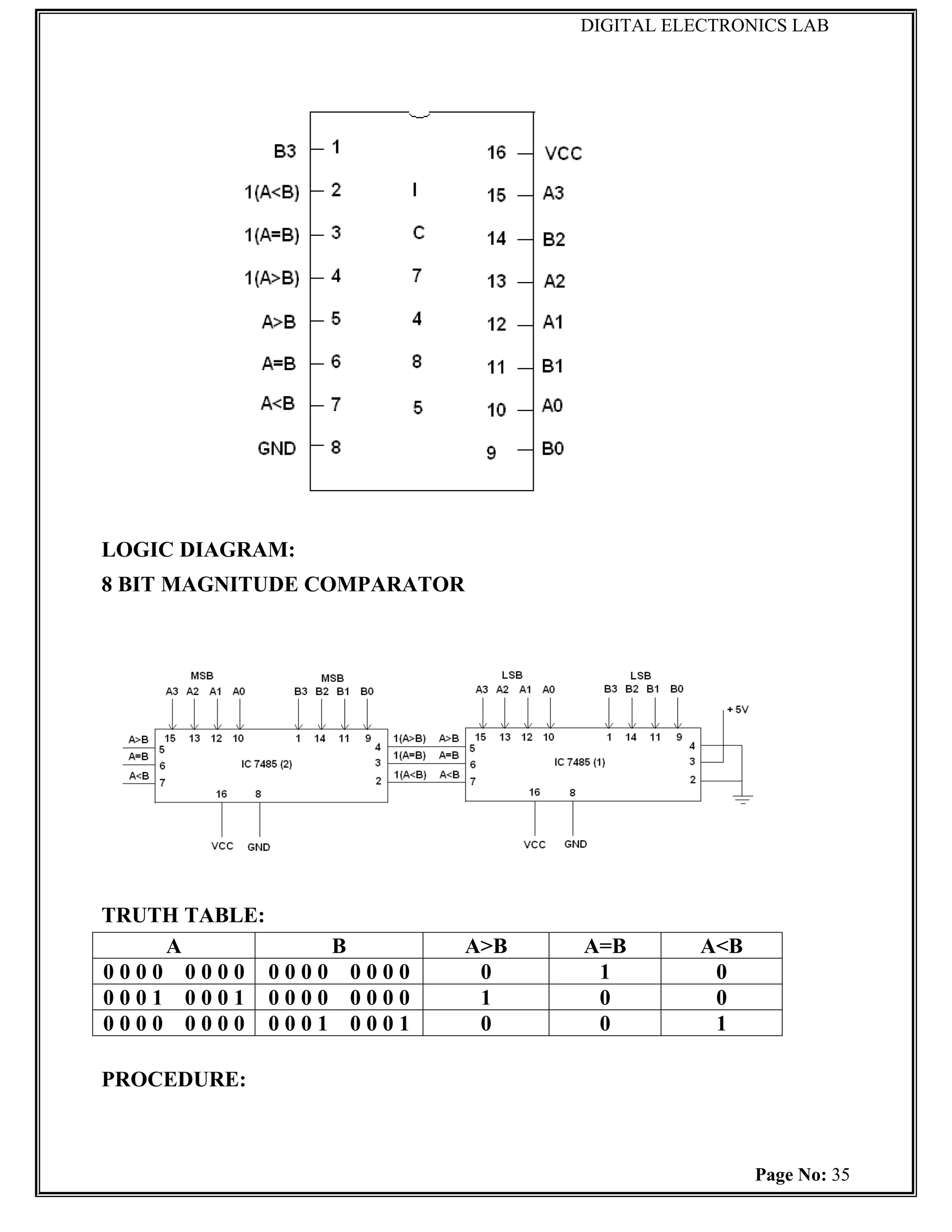
DIGITAL ELECTRONICS LAB
LOGICDIAGRAM:
8 BIT MAGNITUDE COMPARATOR
TRUTH TABLE:
A B A>B A=B A<B
0000 0000 0000 0000 0 1 0
0001 0001 0000 0000 1 0 0
0000 0000 0001 0001 0 0 1
PROCEDURE:
Page No: 35
33.
DIGITAL ELECTRONICS LAB
(i) Connections are given as per circuit diagram.
(ii) Logical inputs are given as per circuit diagram.
(iii) Observe the output and verify the truth table.
RESULT:
Thus the 2-bit and 8-bit magnitude comparator circuits are implemented using
logic gates and IC 7485.
Page No: 36
34.
DIGITAL ELECTRONICS LAB
Ex.No: 6
16 BIT ODD/EVEN PARITY CHECKER /GENERATOR
Date:
AIM:
To design and implement 16 bit odd/even parity checker and generator using
IC 74180.
APPARATUS REQUIRED:
Sl.No. COMPONENT SPECIFICATION QTY.
1. NOT GATE IC 7404 1
1. PARITY IC IC 74180 2
2. IC TRAINER KIT - 1
3. PATCH CORDS - 30
THEORY:
A parity bit is used for detecting errors during transmission of binary
information. A parity bit is an extra bit included with a binary message to make the
number is either even or odd. The message including the parity bit is transmitted and
then checked at the receiver ends for errors. An error is detected if the checked parity
bit doesn’t correspond to the one transmitted. The circuit that generates the parity bit
in the transmitter is called a ‘parity generator’ and the circuit that checks the parity in
the receiver is called a ‘parity checker’.
In even parity, the added parity bit will make the total number is even amount.
In odd parity, the added parity bit will make the total number is odd amount. The
parity checker circuit checks for possible errors in the transmission. If the information
is passed in even parity, then the bits required must have an even number of 1’s. An
error occur during transmission, if the received bits have an odd number of 1’s
indicating that one bit has changed in value during transmission.
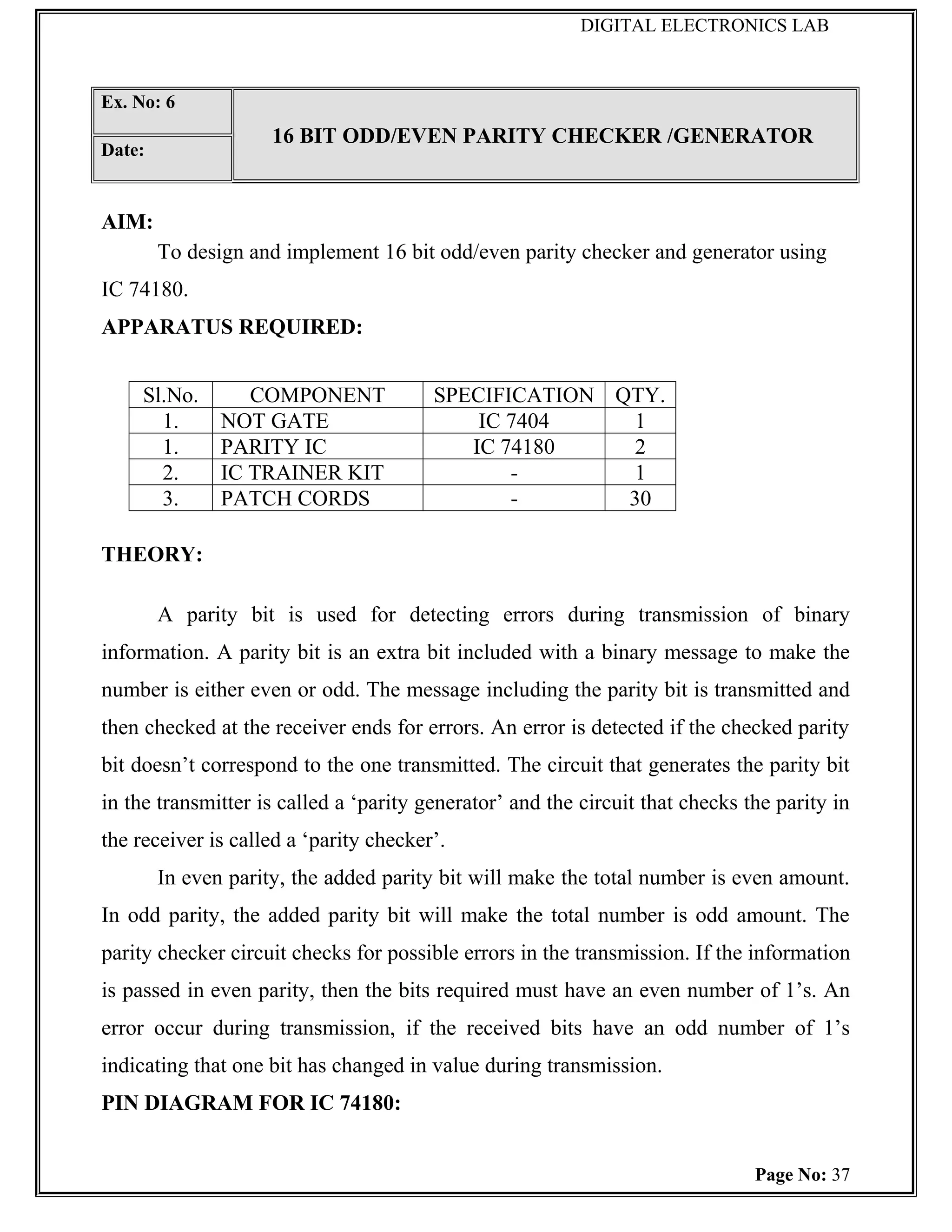
PIN DIAGRAM FOR IC 74180:
Page No: 37
35.
DIGITAL ELECTRONICS LAB
FUNCTIONTABLE:
INPUTS OUTPUTS
Number of High Data PE PO ∑E ∑O
Inputs (I0 – I7)
EVEN 1 0 1 0
ODD 1 0 0 1
EVEN 0 1 0 1
ODD 0 1 1 0
X 1 1 0 0
X 0 0 1 1
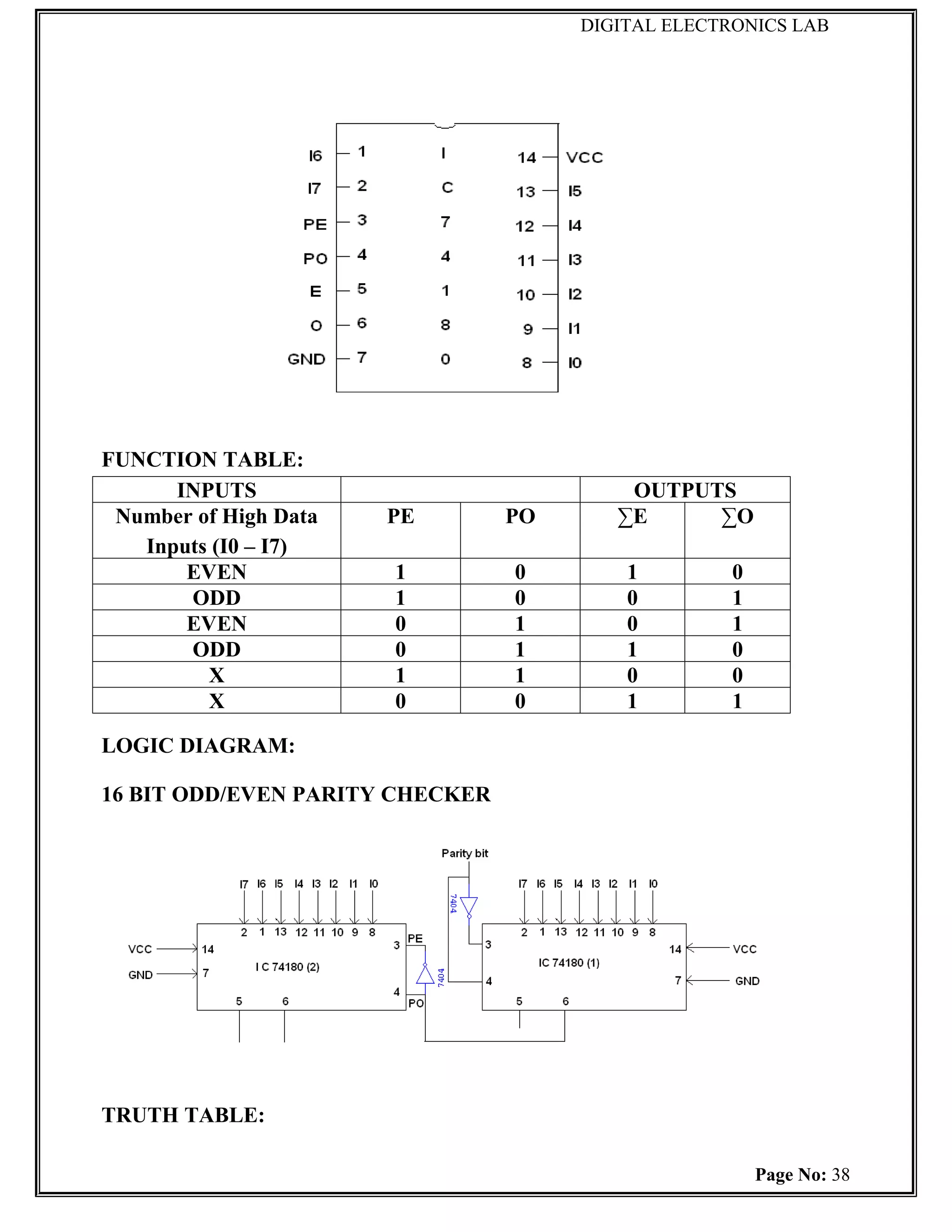
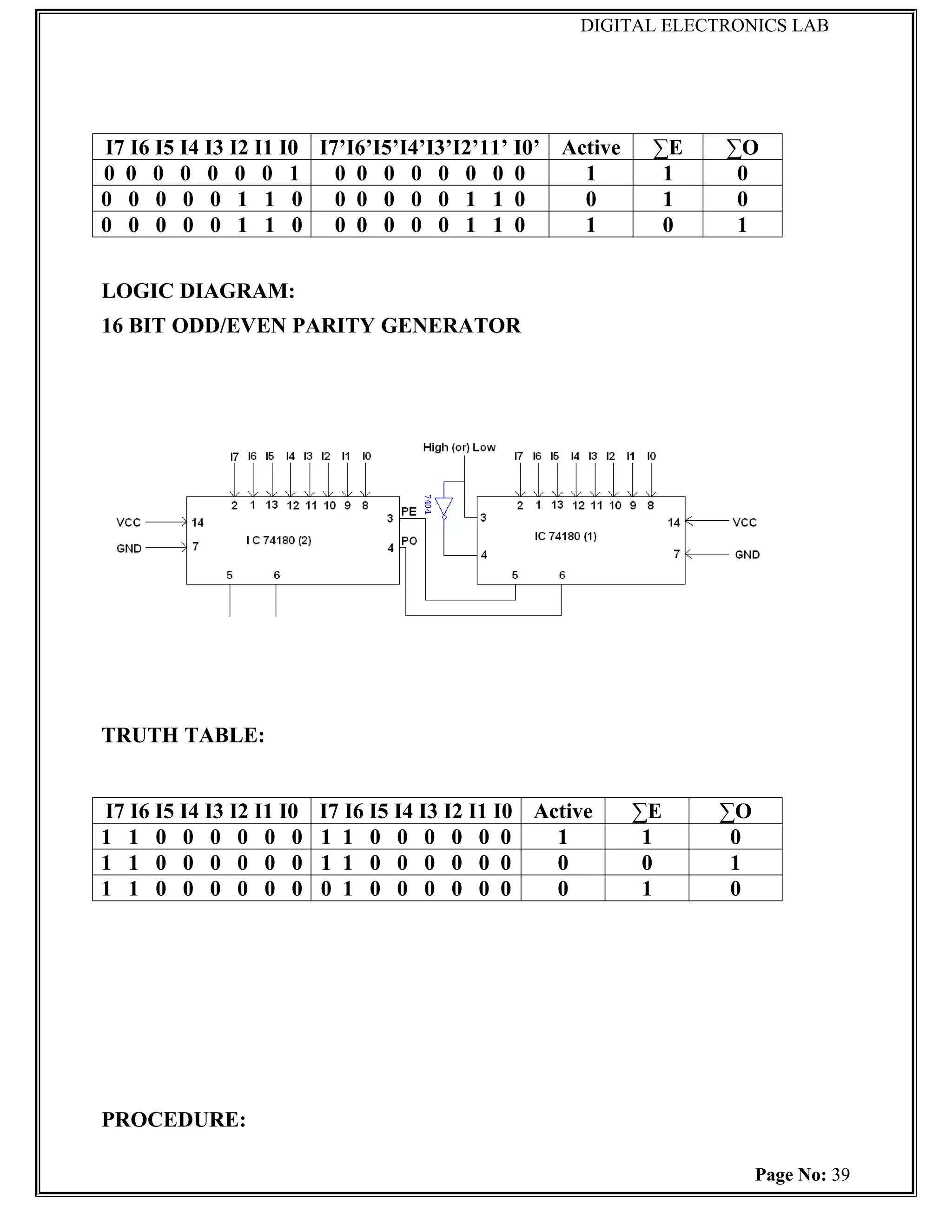
LOGIC DIAGRAM:
16 BIT ODD/EVEN PARITY CHECKER
TRUTH TABLE:
Page No: 38
DIGITAL ELECTRONICS LAB
(i) Connections are given as per circuit diagram.
(ii) Logical inputs are given as per circuit diagram.
(iii) Observe the output and verify the truth table.
RESULT:
Thus the 16 bit odd/even parity checker and generator circuit designed and
implemented using IC 74180.
Ex. No: 7
Page No: 40
38.
DIGITAL ELECTRONICS LAB
Date: DESIGN AND IMPLEMENTATION OF MULTIPLEXER AND
DEMULTIPLEXER
AIM:
To design and implement multiplexer and demultiplexer using logic gates and
study of IC 74150 and IC 74154.
APPARATUS REQUIRED:
Sl.No. COMPONENT SPECIFICATION QTY.
1. 3 I/P AND GATE IC 7411 2
2. OR GATE IC 7432 1
3. NOT GATE IC 7404 1
2. IC TRAINER KIT - 1
3. PATCH CORDS - 32
THEORY:
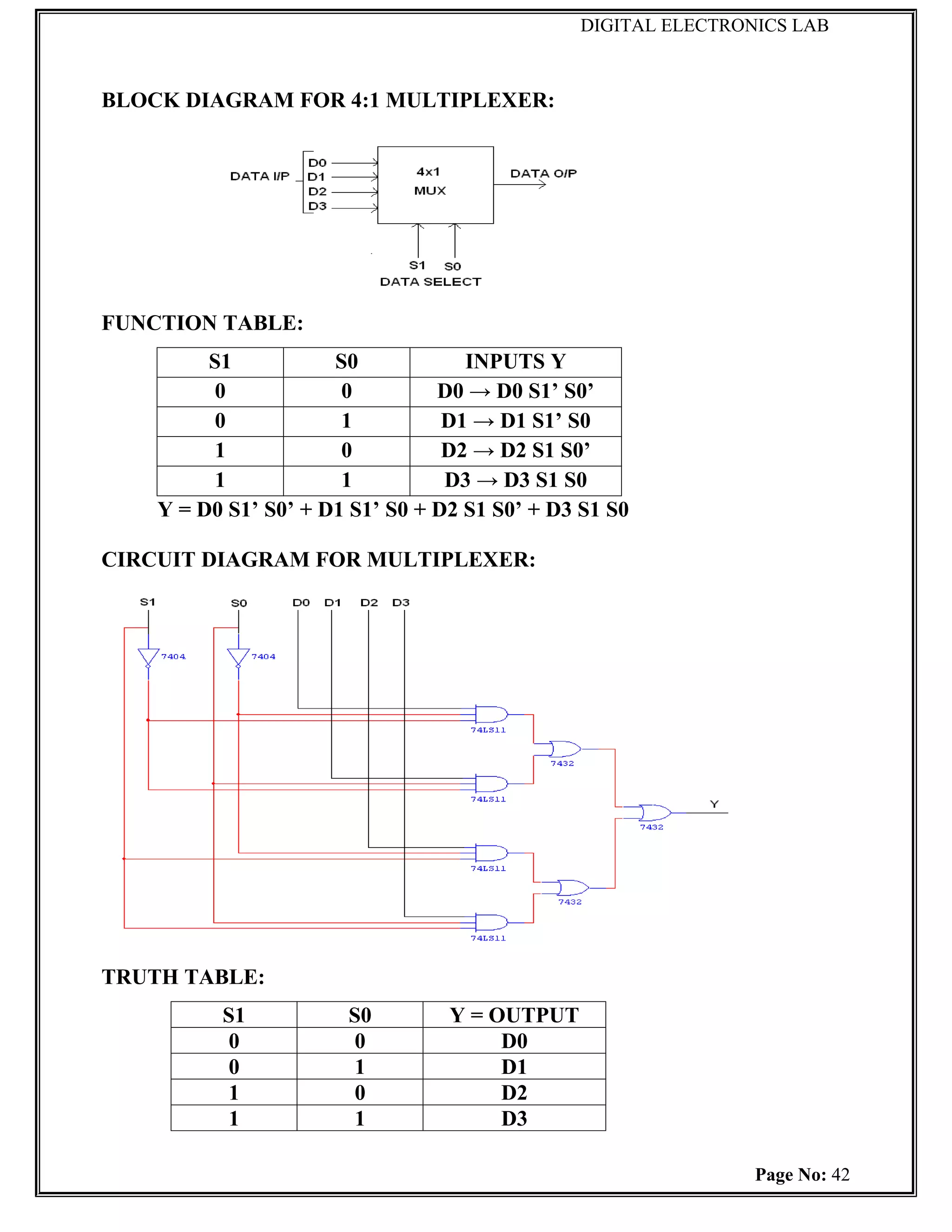
MULTIPLEXER:
Multiplexer means transmitting a large number of information units over a
smaller number of channels or lines. A digital multiplexer is a combinational circuit
that selects binary information from one of many input lines and directs it to a single
output line. The selection of a particular input line is controlled by a set of selection
lines. Normally there are 2n input line and n selection lines whose bit combination
determine which input is selected.
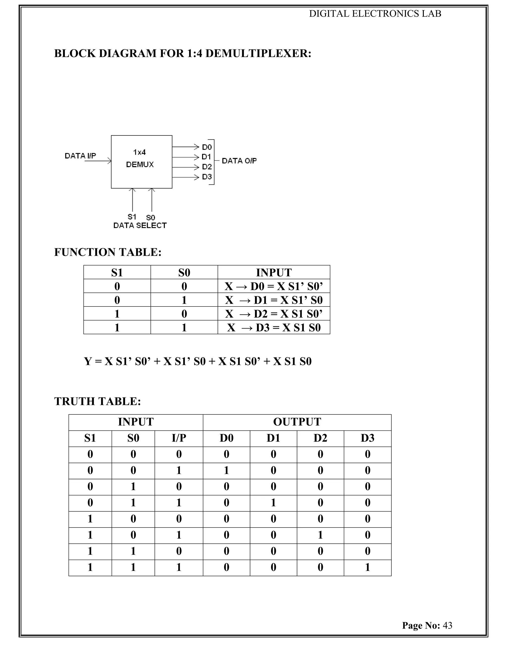
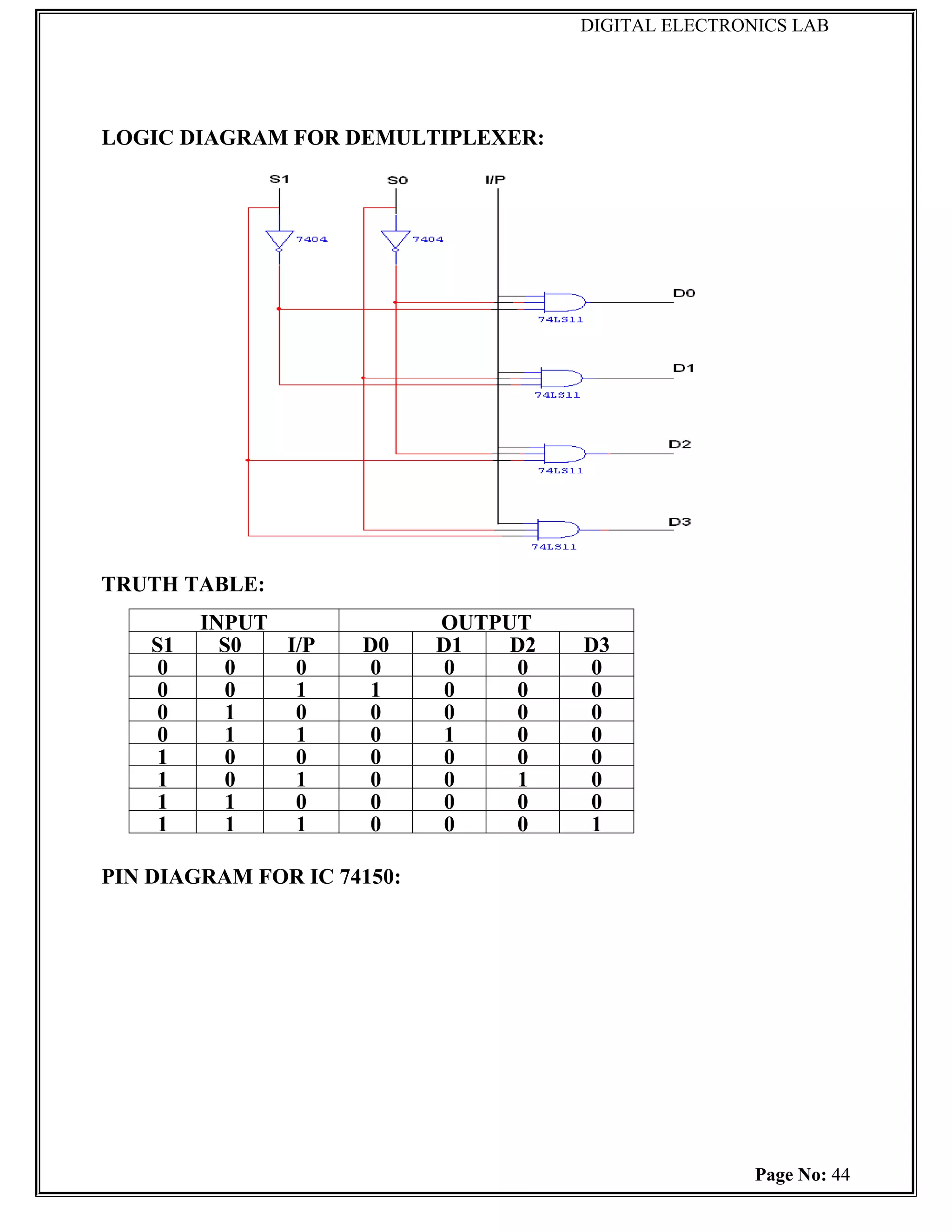
DEMULTIPLEXER:
The function of Demultiplexer is in contrast to multiplexer function. It takes
information from one line and distributes it to a given number of output lines. For this
reason, the demultiplexer is also known as a data distributor. Decoder can also be
used as demultiplexer. In the 1: 4 demultiplexer circuit, the data input line goes to all
of the AND gates. The data select lines enable only one gate at a time and the data on
the data input line will pass through the selected gate to the associated data output
line.
Page No: 41
DIGITAL ELECTRONICS LAB
PINDIAGRAM FOR IC 74154:
PROCEDURE:
(i) Connections are given as per circuit diagram.
(ii) Logical inputs are given as per circuit diagram.
(iii) Observe the output and verify the truth table.
Page No: 45
43.
DIGITAL ELECTRONICS LAB
RESULT:
Thus the multiplexer and demultiplexer circuits are designed and implemented
using logic gates, IC 74150 and IC 74154.
Ex. No: 8
DESIGN AND IMPLEMENTATION OF ENCODER AND
Date:
DECODER
AIM:
To design and implement encoder and decoder using logic gates and study of
IC 7445 and IC 74147.
APPARATUS REQUIRED:
Sl.No. COMPONENT SPECIFICATION QTY.
1. 3 I/P NAND GATE IC 7410 2
2. OR GATE IC 7432 3
3. NOT GATE IC 7404 1
2. IC TRAINER KIT - 1
3. PATCH CORDS - 27
THEORY:
ENCODER:
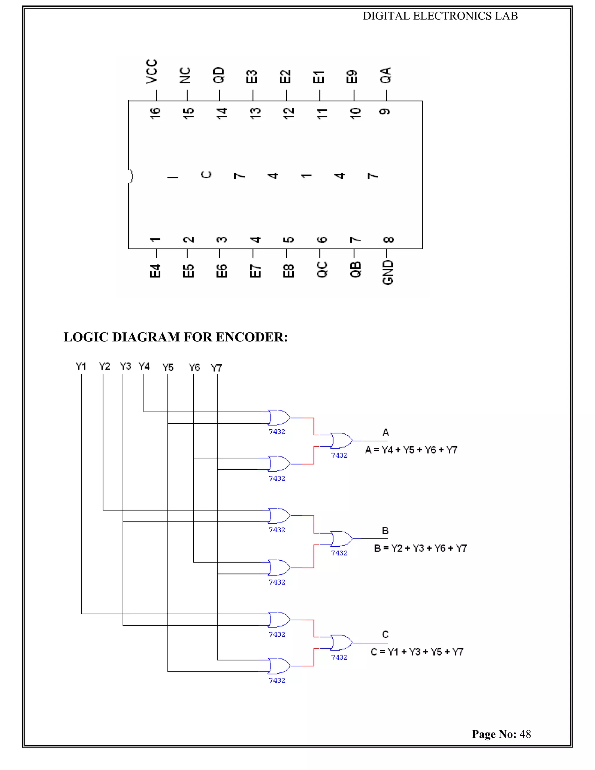
An encoder is a digital circuit that perform inverse operation of a decoder. An
encoder has 2n input lines and n output lines. In encoder the output lines generates the
binary code corresponding to the input value. In octal to binary encoder it has eight
inputs, one for each octal digit and three output that generate the corresponding
binary code. In encoder it is assumed that only one input has a value of one at any
given time otherwise the circuit is meaningless. It has an ambiguila that when all
Page No: 46
44.
DIGITAL ELECTRONICS LAB
inputsare zero the outputs are zero. The zero outputs can also be generated when D0
= 1.
DECODER:
A decoder is a multiple input multiple output logic circuit which converts
coded input into coded output where input and output codes are different. The input
code generally has fewer bits than the output code. Each input code word produces a
different output code word i.e there is one to one mapping can be expressed in truth
table. In the block diagram of decoder circuit the encoded information is present as n
input producing 2n possible outputs. 2n output values are from 0 through out 2n – 1.
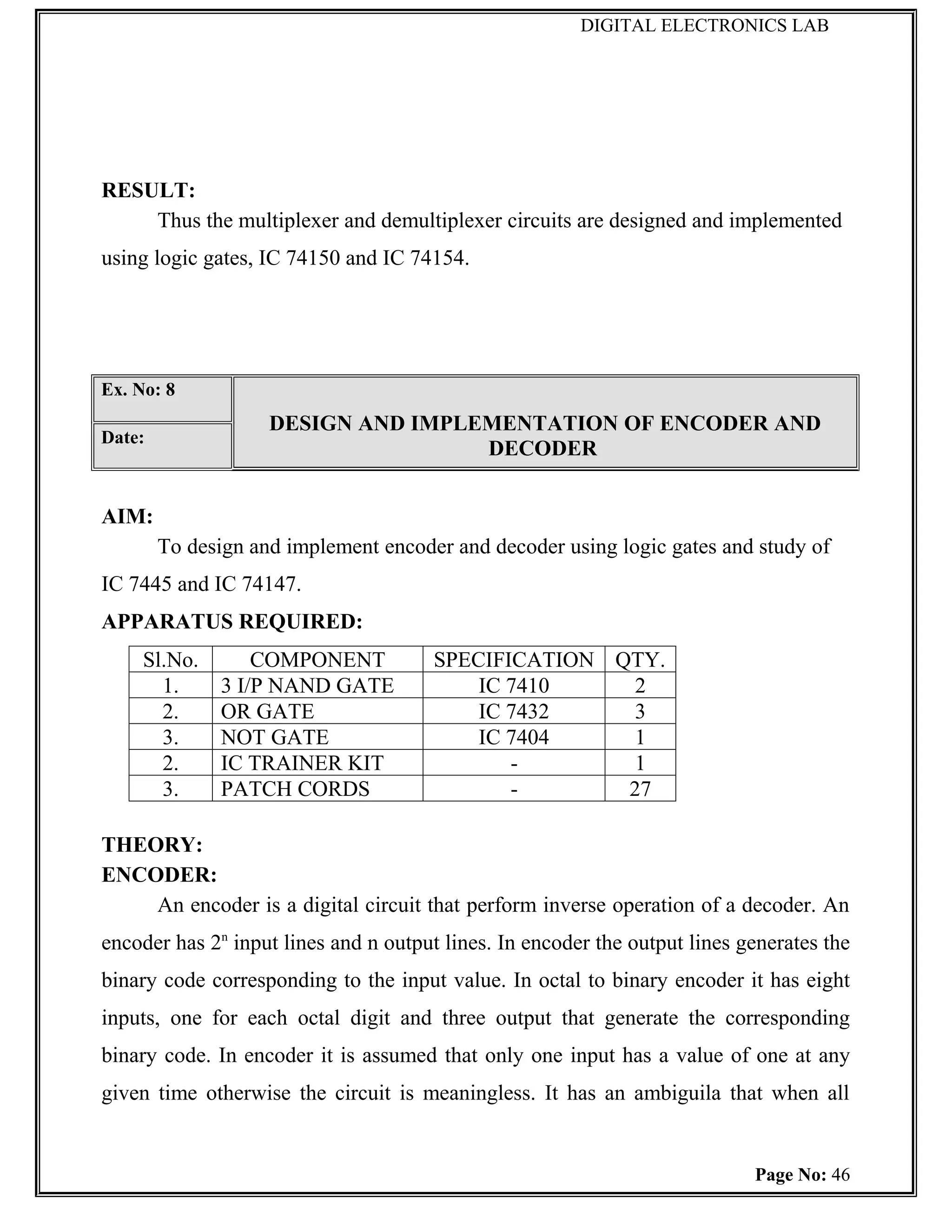
PIN DIAGRAM FOR IC 7445:
BCD TO DECIMAL DECODER:
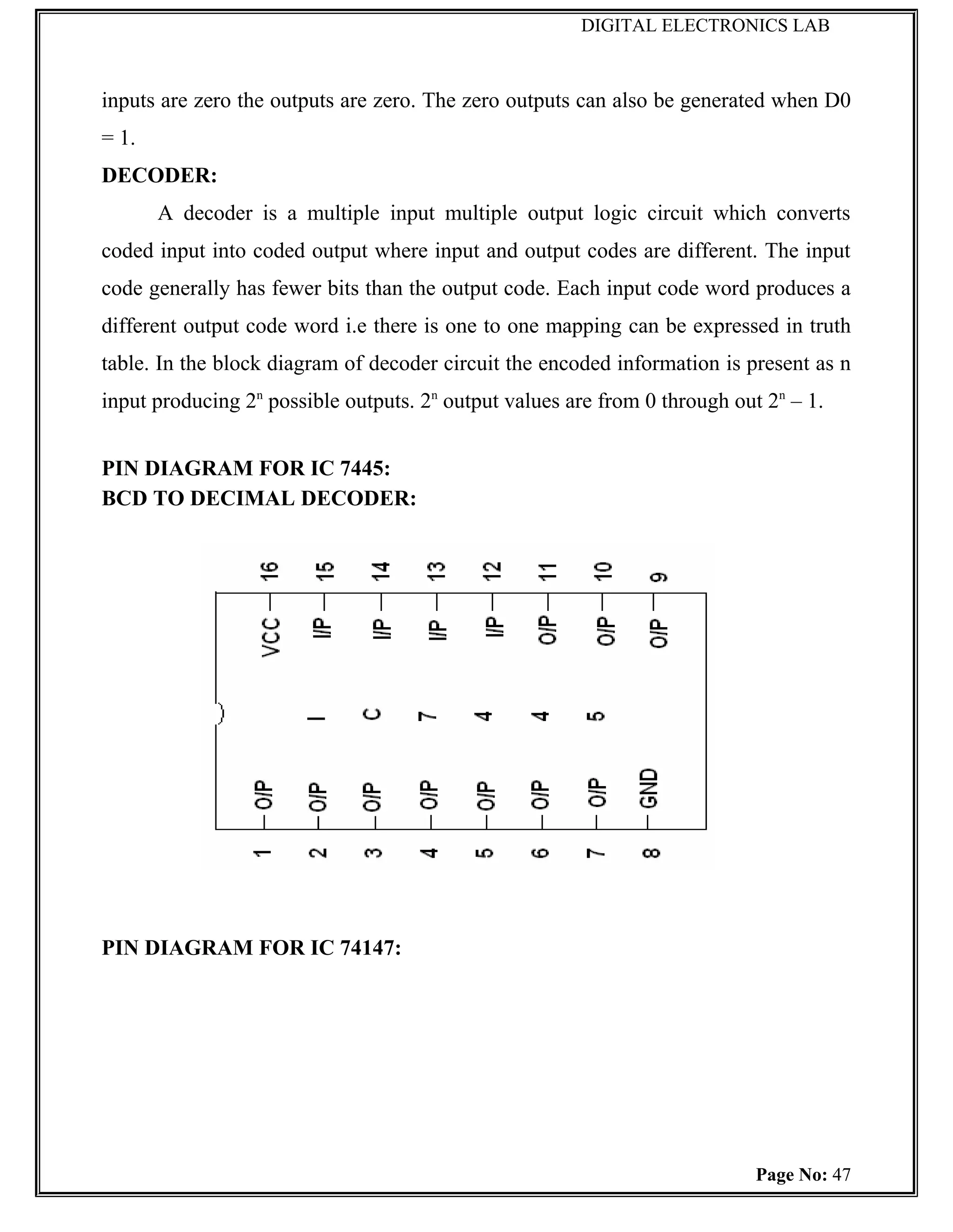
PIN DIAGRAM FOR IC 74147:
Page No: 47
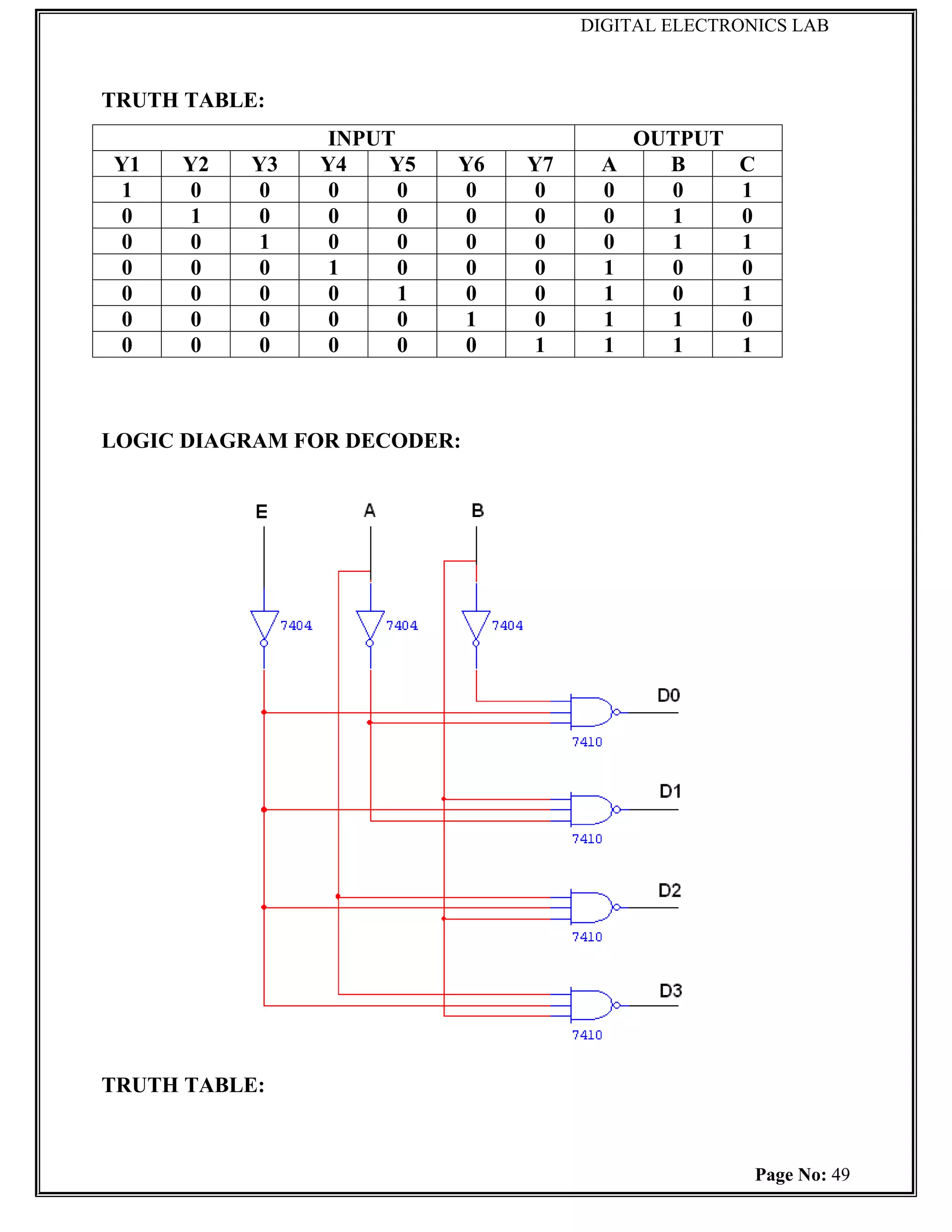
DIGITAL ELECTRONICS LAB
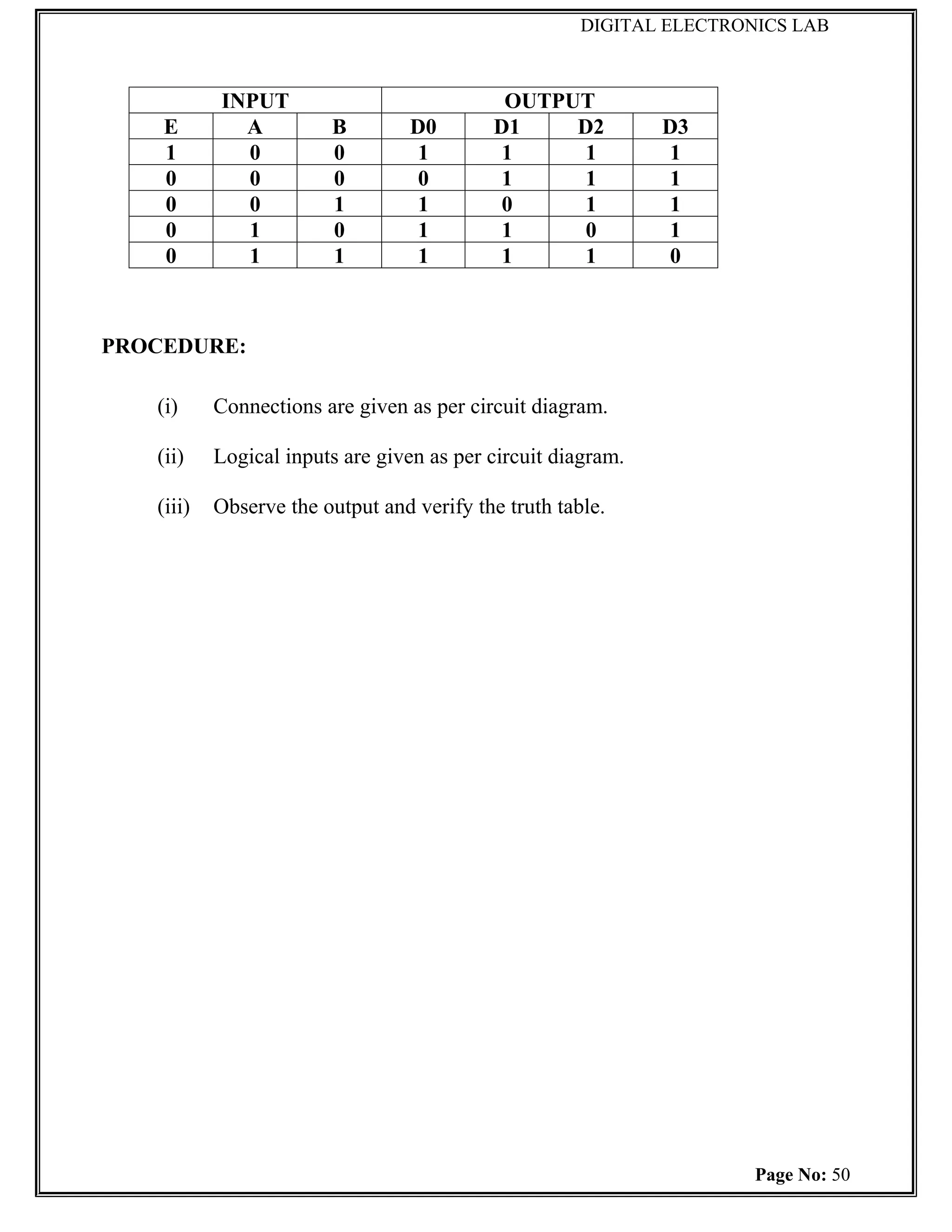
INPUT OUTPUT
E A B D0 D1 D2 D3
1 0 0 1 1 1 1
0 0 0 0 1 1 1
0 0 1 1 0 1 1
0 1 0 1 1 0 1
0 1 1 1 1 1 0
PROCEDURE:
(i) Connections are given as per circuit diagram.
(ii) Logical inputs are given as per circuit diagram.
(iii) Observe the output and verify the truth table.
Page No: 50
48.
DIGITAL ELECTRONICS LAB
RESULT:
Thus the encoder and decoder circuits were designed and implemented using
logic gates, IC 7445 and IC 74147.
Ex. No: 9
CONSTRUCTION AND VERIFICATION OF 4 BIT RIPPLE
Date: COUNTER AND MOD 10/MOD 12 RIPPLE COUNTER
AIM:
To design and verify 4 bit ripple counter mod 10/ mod 12 ripple counter.
APPARATUS REQUIRED:
Sl.No. COMPONENT SPECIFICATION QTY.
1. JK FLIP FLOP IC 7476 2
2. NAND GATE IC 7400 1
3. IC TRAINER KIT - 1
4. PATCH CORDS - 30
THEORY:
A counter is a register capable of counting number of clock pulse arriving at its
clock input. Counter represents the number of clock pulses arrived. A specified
sequence of states appears as counter output. This is the main difference between a
register and a counter. In synchronous common clock is given to all flip flop and in
asynchronous first flip flop is clocked by external pulse and then each successive flip
flop is clocked by Q or Q output of previous stage. Because of inherent propagation
delay time all flip flops are not activated at same time which results in asynchronous
operation.
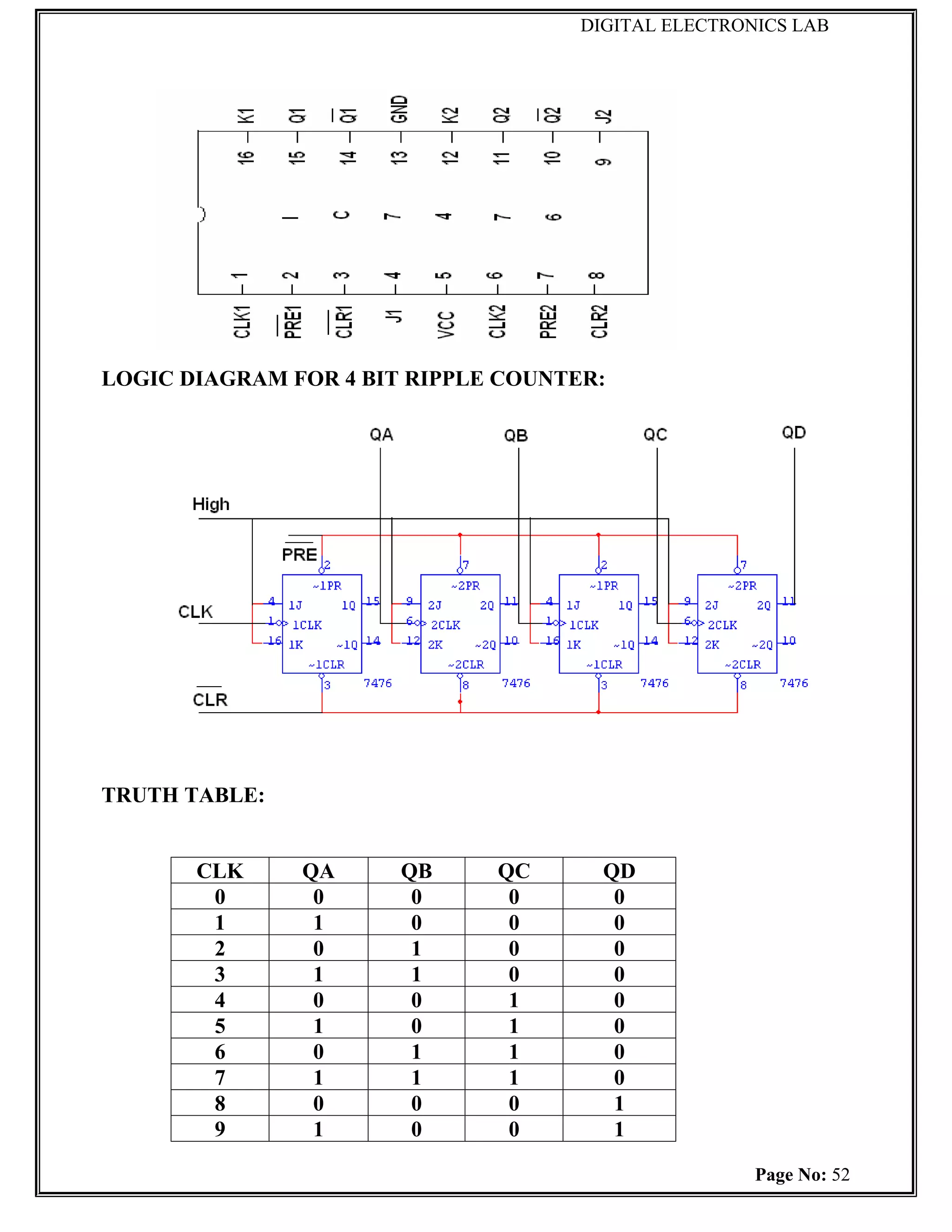
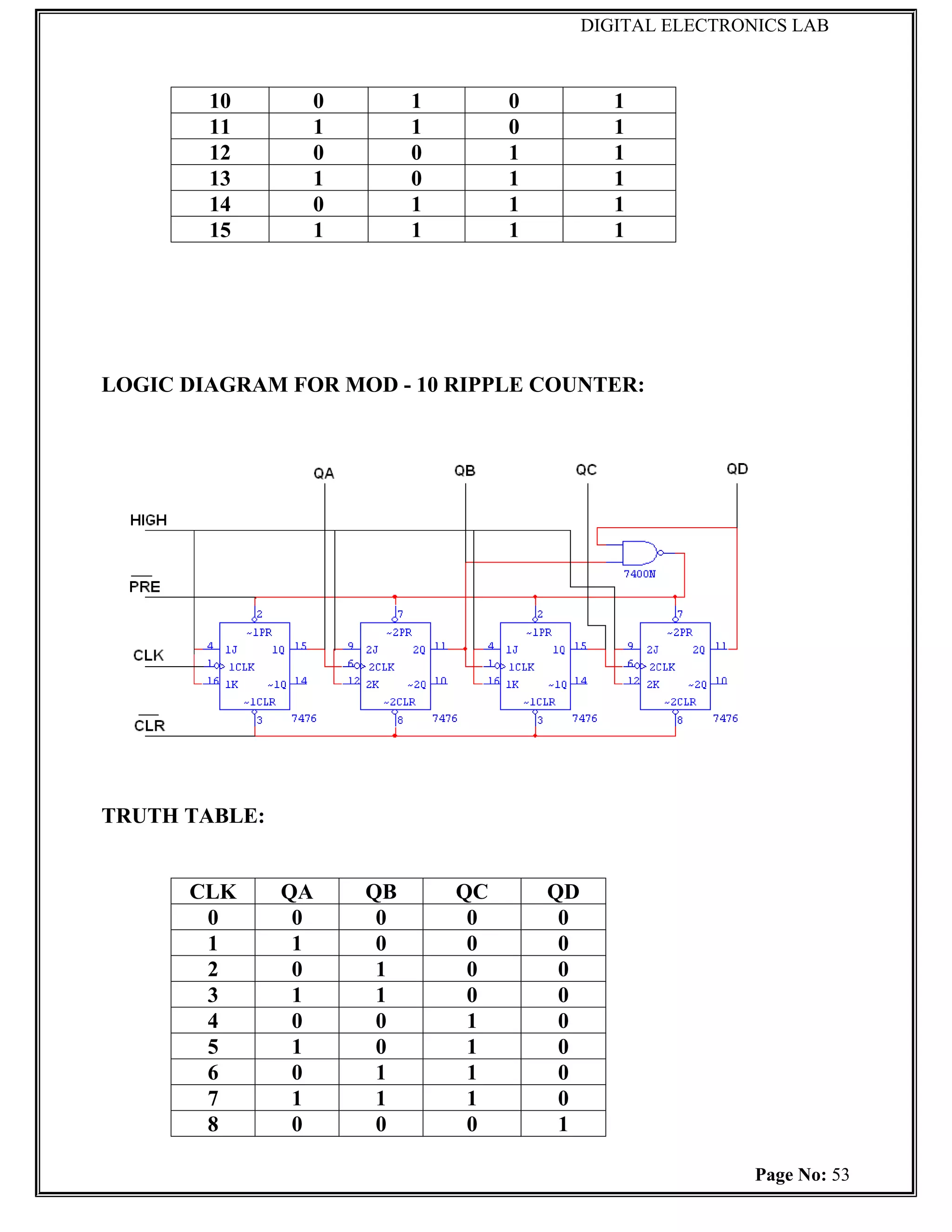
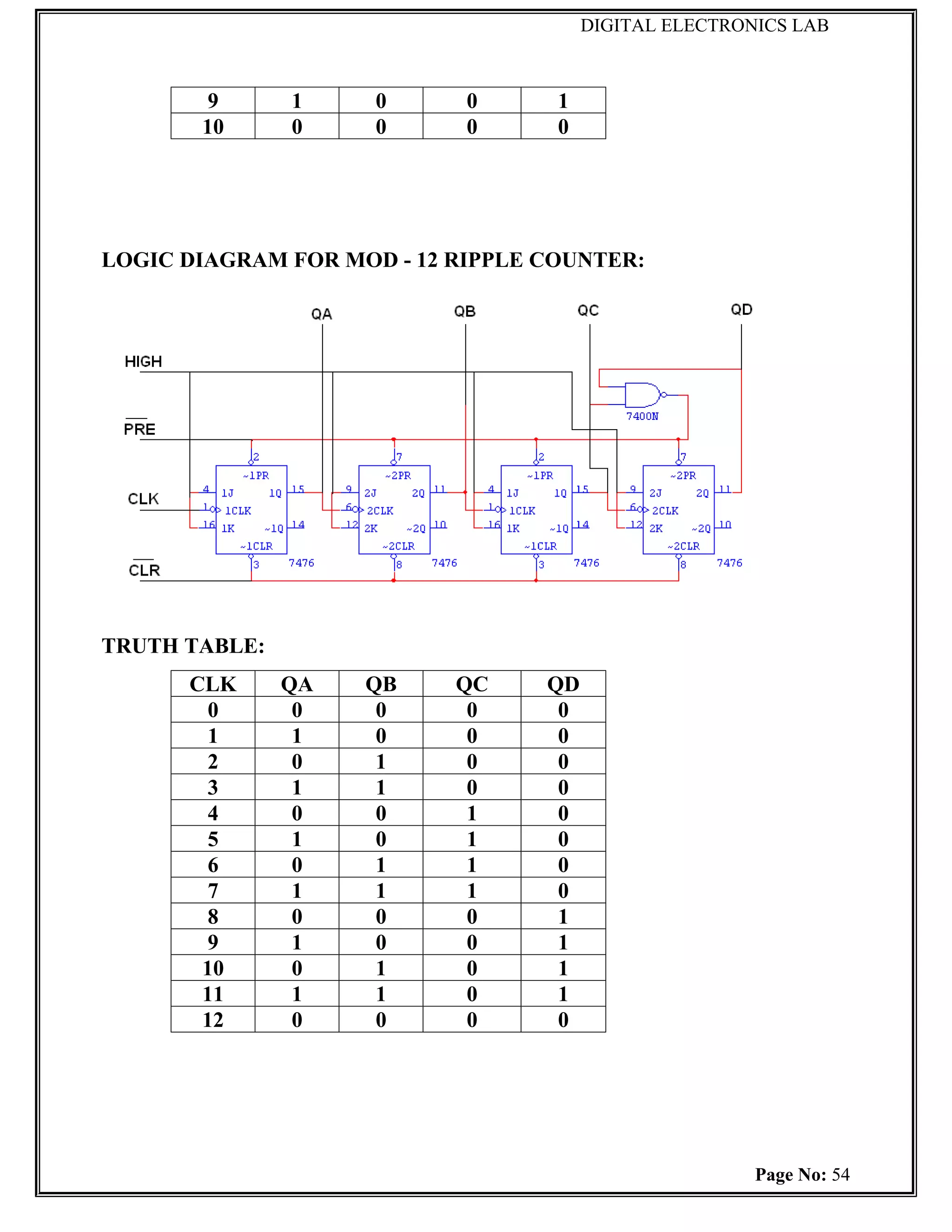
PIN DIAGRAM FOR IC 7476:
Page No: 51
DIGITAL ELECTRONICS LAB
PROCEDURE:
(i) Connections are given as per circuit diagram.
(ii) Logical inputs are given as per circuit diagram.
(iii) Observe the output and verify the truth table.
RESULT:
Thus the 4 bit ripple counter mod 10/ mod 12 ripple counter circuits were
designed and verified successfully.
Page No: 55
53.
DIGITAL ELECTRONICS LAB
Ex.No: 10
DESIGN AND IMPLEMENTATION OF 3 BIT
Date: SYNCHRONOUS UP/DOWN COUNTER
AIM:
To design and implement 3 bit synchronous up/down counter.
APPARATUS REQUIRED:
Sl.No. COMPONENT SPECIFICATION QTY.
1. JK FLIP FLOP IC 7476 2
2. 3 I/P AND GATE IC 7411 1
3. OR GATE IC 7432 1
4. XOR GATE IC 7486 1
5. NOT GATE IC 7404 1
6. IC TRAINER KIT - 1
7. PATCH CORDS - 35
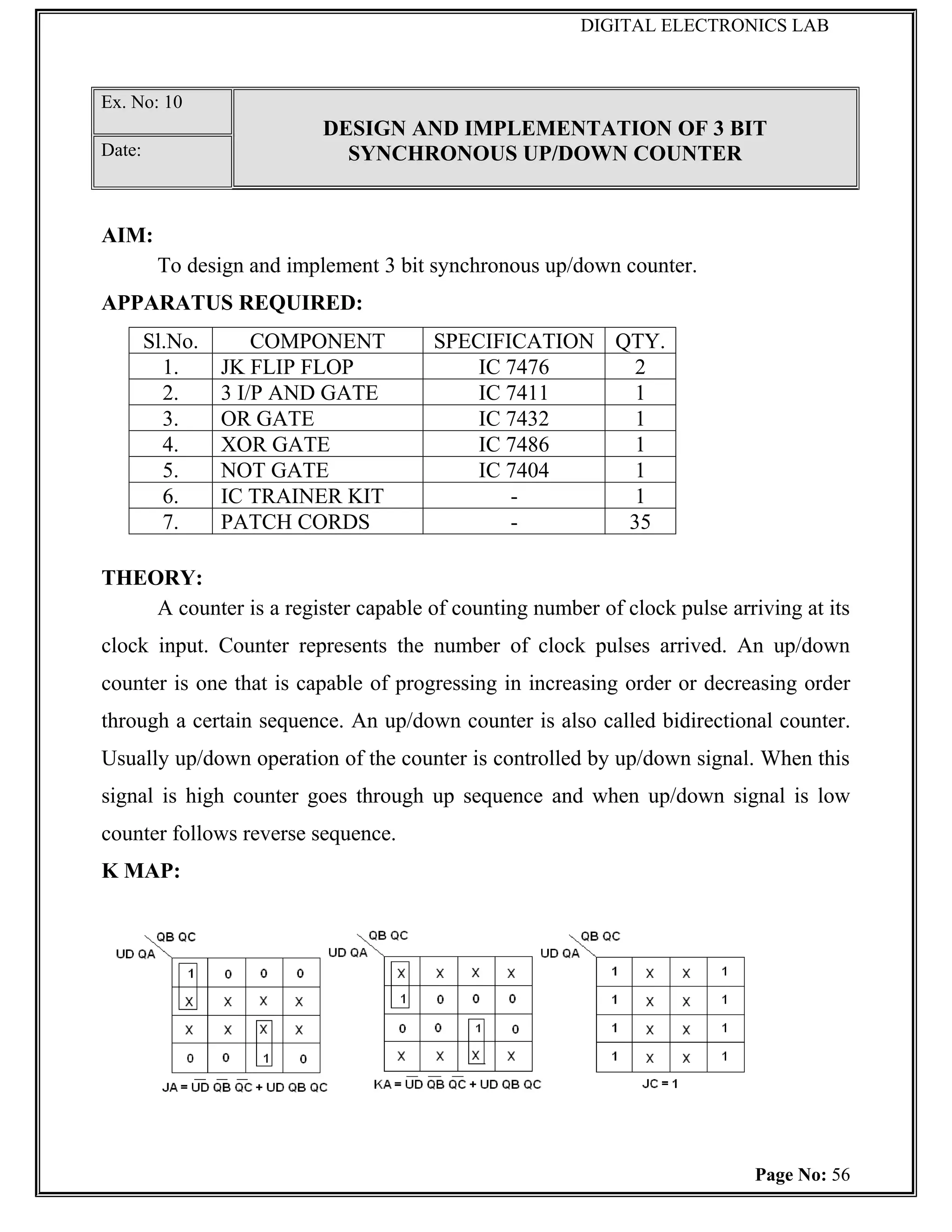
THEORY:
A counter is a register capable of counting number of clock pulse arriving at its
clock input. Counter represents the number of clock pulses arrived. An up/down
counter is one that is capable of progressing in increasing order or decreasing order
through a certain sequence. An up/down counter is also called bidirectional counter.
Usually up/down operation of the counter is controlled by up/down signal. When this
signal is high counter goes through up sequence and when up/down signal is low
counter follows reverse sequence.
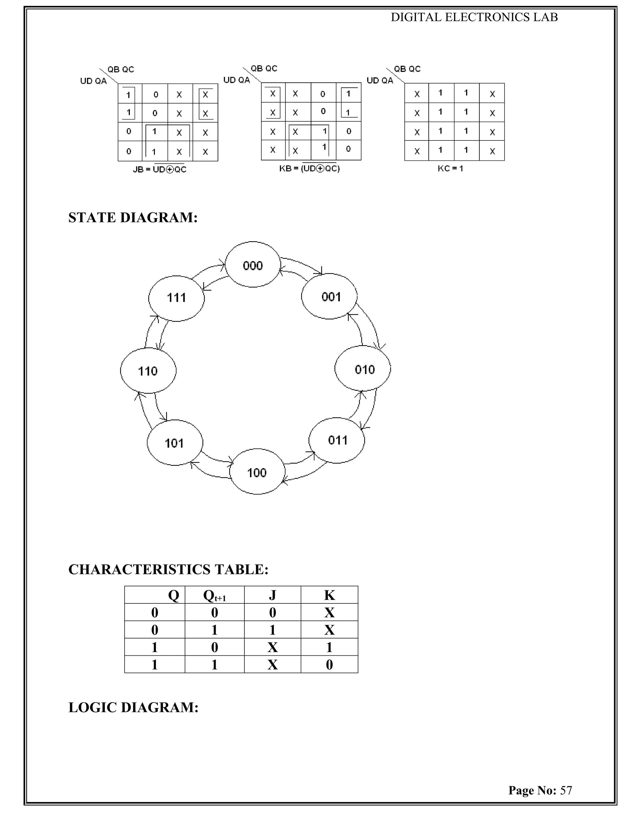
K MAP:
Page No: 56
54.
DIGITAL ELECTRONICS LAB
STATEDIAGRAM:
CHARACTERISTICS TABLE:
Q Qt+1 J K
0 0 0 X
0 1 1 X
1 0 X 1
1 1 X 0
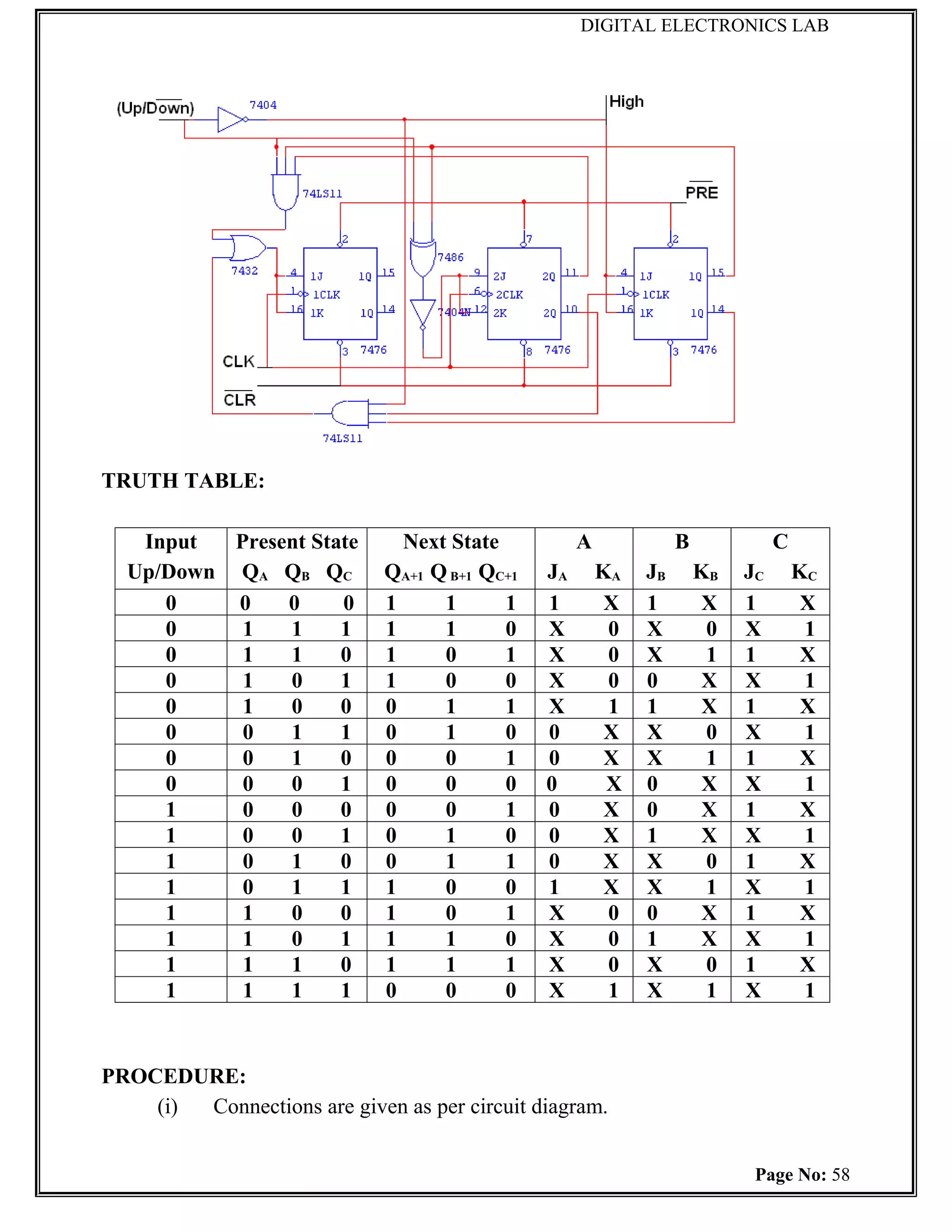
LOGIC DIAGRAM:
Page No: 57
55.
DIGITAL ELECTRONICS LAB
TRUTHTABLE:
Input Present State Next State A B C
Up/Down QA QB QC QA+1 Q B+1 QC+1 JA KA JB KB JC KC
0 0 0 0 1 1 1 1 X 1 X 1 X
0 1 1 1 1 1 0 X 0 X 0 X 1
0 1 1 0 1 0 1 X 0 X 1 1 X
0 1 0 1 1 0 0 X 0 0 X X 1
0 1 0 0 0 1 1 X 1 1 X 1 X
0 0 1 1 0 1 0 0 X X 0 X 1
0 0 1 0 0 0 1 0 X X 1 1 X
0 0 0 1 0 0 0 0 X 0 X X 1
1 0 0 0 0 0 1 0 X 0 X 1 X
1 0 0 1 0 1 0 0 X 1 X X 1
1 0 1 0 0 1 1 0 X X 0 1 X
1 0 1 1 1 0 0 1 X X 1 X 1
1 1 0 0 1 0 1 X 0 0 X 1 X
1 1 0 1 1 1 0 X 0 1 X X 1
1 1 1 0 1 1 1 X 0 X 0 1 X
1 1 1 1 0 0 0 X 1 X 1 X 1
PROCEDURE:
(i) Connections are given as per circuit diagram.
Page No: 58
56.
DIGITAL ELECTRONICS LAB
(ii) Logical inputs are given as per circuit diagram.
(iii) Observe the output and verify the truth table.
RESULT:
Thus the 3 bit synchronous up/down counter was designed and implemented
using the IC7476.
Ex. No: 11
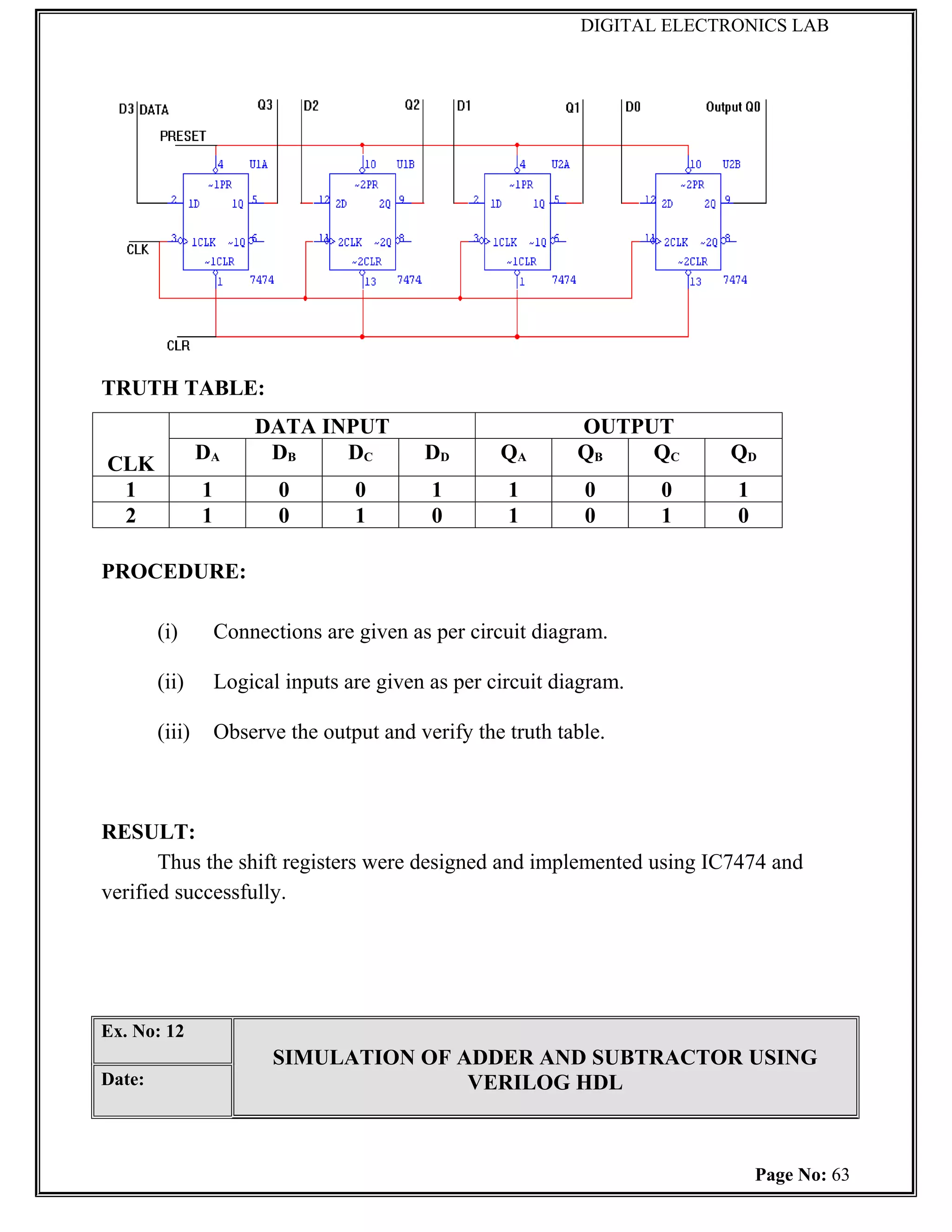
DESIGN AND IMPLEMENTATION OF SHIFT REGISTER
Date:
Page No: 59
57.
DIGITAL ELECTRONICS LAB
AIM:
To design and implement
(i) Serial in serial out
(ii) Serial in parallel out
(iii) Parallel in serial out
(iv) Parallel in parallel out
APPARATUS REQUIRED:
Sl.No. COMPONENT SPECIFICATION QTY.
1. D FLIP FLOP IC 7474 2
2. OR GATE IC 7432 1
3. IC TRAINER KIT - 1
4. PATCH CORDS - 35
THEORY:
A register is capable of shifting its binary information in one or both directions
is known as shift register. The logical configuration of shift register consist of a D-
Flip flop cascaded with output of one flip flop connected to input of next flip flop.
All flip flops receive common clock pulses which causes the shift in the output of the
flip flop. The simplest possible shift register is one that uses only flip flop.
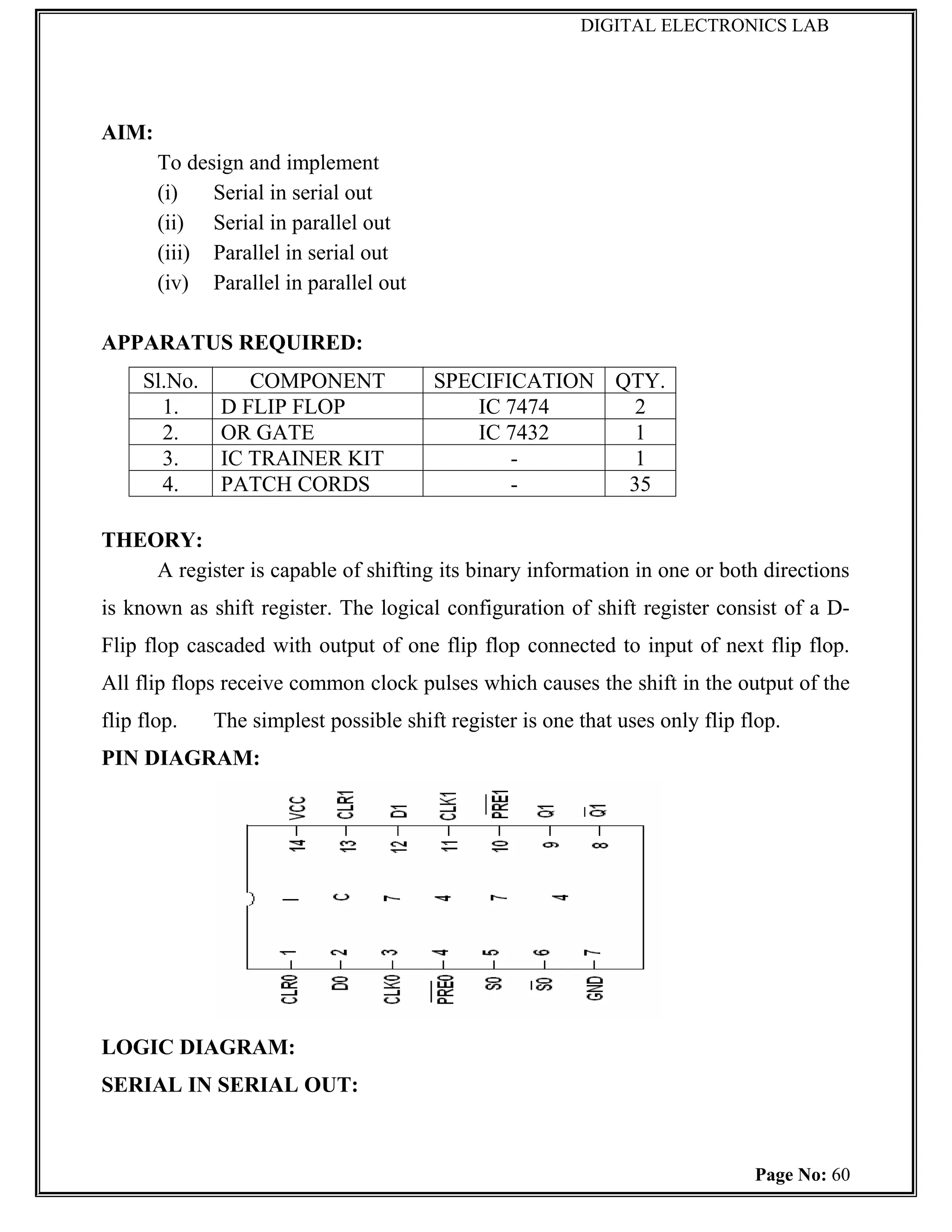
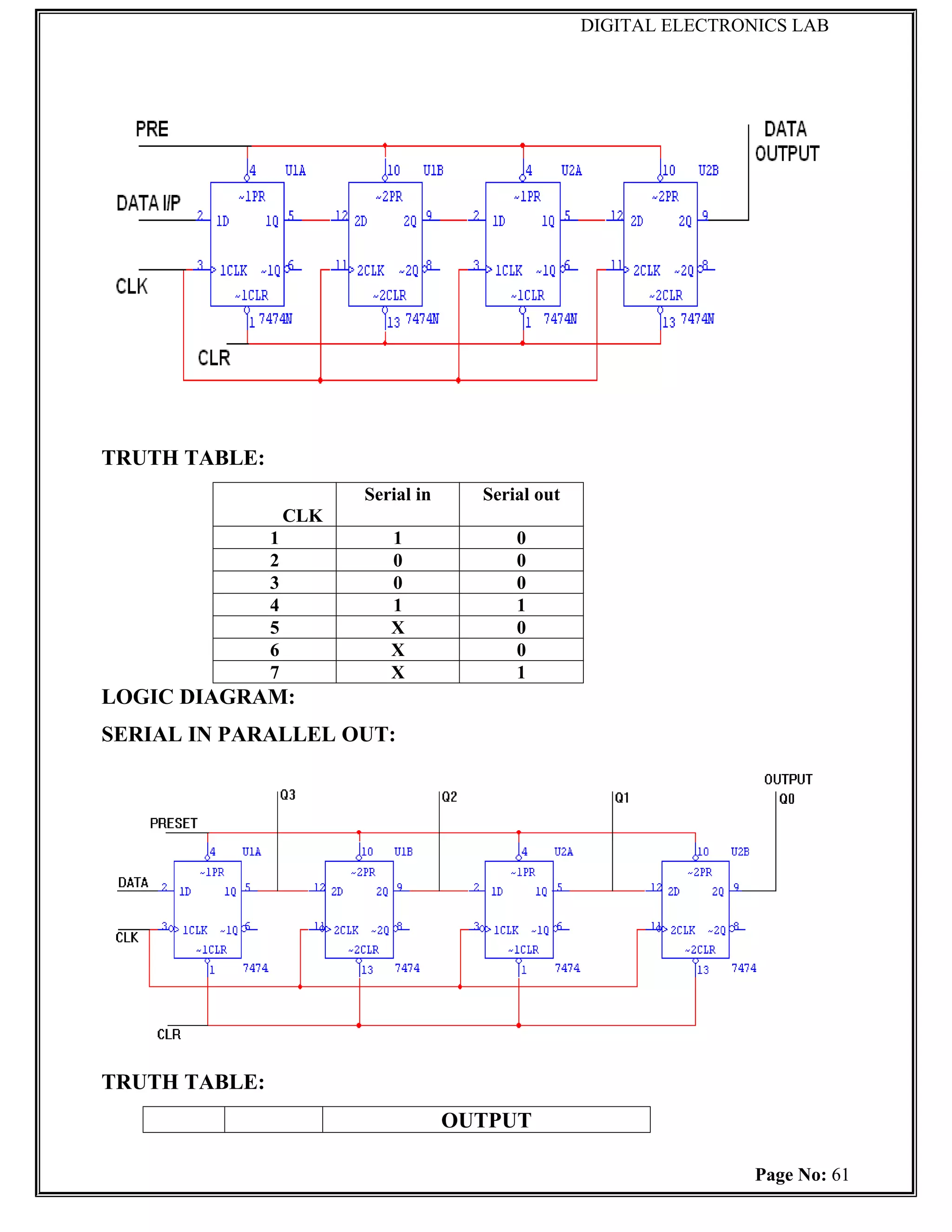
PIN DIAGRAM:
LOGIC DIAGRAM:
SERIAL IN SERIAL OUT:
Page No: 60
58.
DIGITAL ELECTRONICS LAB
TRUTHTABLE:
Serial in Serial out
CLK
1 1 0
2 0 0
3 0 0
4 1 1
5 X 0
6 X 0
7 X 1
LOGIC DIAGRAM:
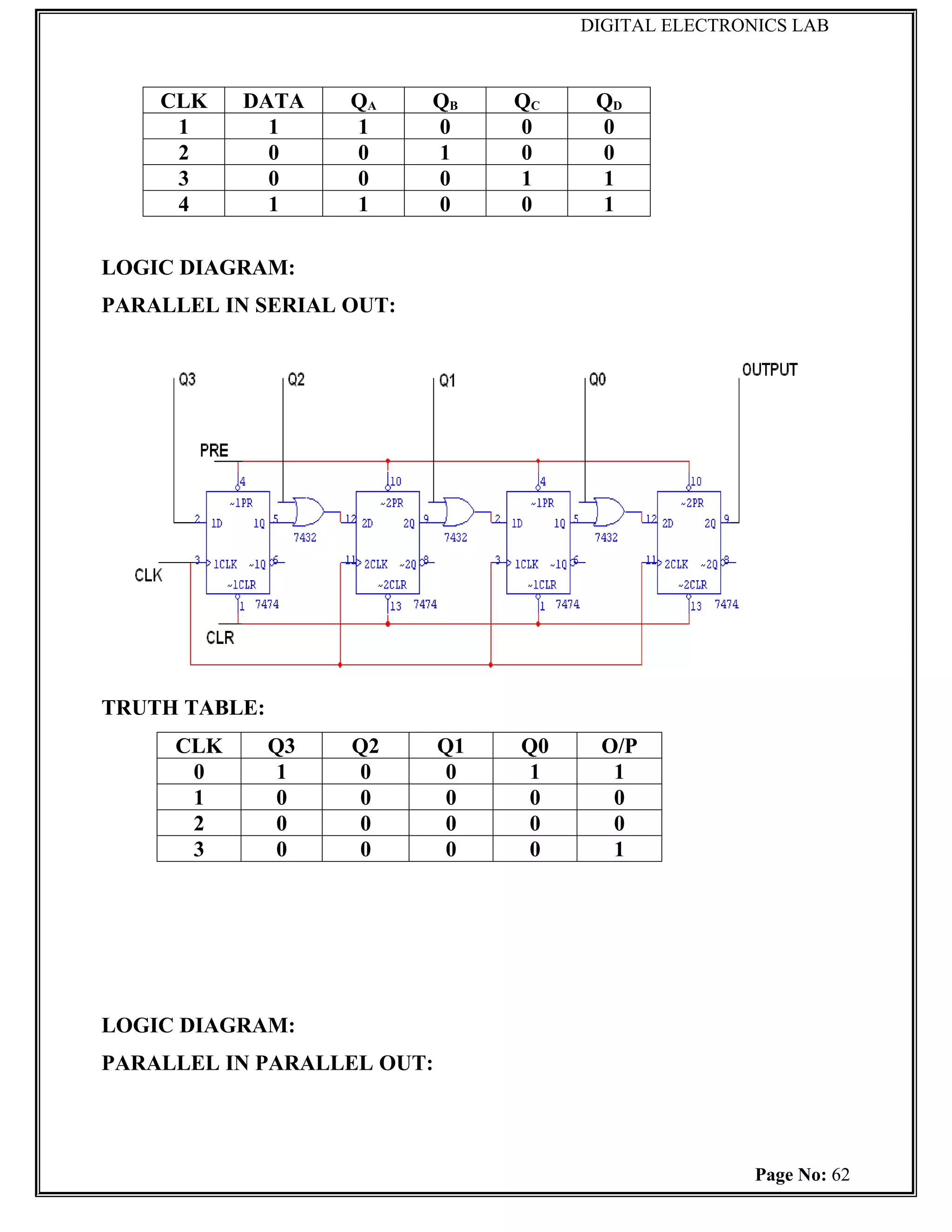
SERIAL IN PARALLEL OUT:
TRUTH TABLE:
OUTPUT
Page No: 61
DIGITAL ELECTRONICS LAB
TRUTHTABLE:
DATA INPUT OUTPUT
DA DB DC DD QA QB QC QD
CLK
1 1 0 0 1 1 0 0 1
2 1 0 1 0 1 0 1 0
PROCEDURE:
(i) Connections are given as per circuit diagram.
(ii) Logical inputs are given as per circuit diagram.
(iii) Observe the output and verify the truth table.
RESULT:
Thus the shift registers were designed and implemented using IC7474 and
verified successfully.
Ex. No: 12
SIMULATION OF ADDER AND SUBTRACTOR USING
Date: VERILOG HDL
Page No: 63
61.
DIGITAL ELECTRONICS LAB
AIM:
To write the Verilog HDL program for adder and subtractor circuit and
simulate it using ISE simulator.
HARDWARE& SOFTWARE REQUIRED:
XILINK 9.1i Simulator
PC WITH WINDOWS-XP
THEORY:
HALF ADDER:
From the verbal explanation of a half adder, we find that this circuit needs two
binary inputs and two binary outputs. The input variables designate the augends and
addend bits; the output variables produce the sum and carry. We assign symbol ‘a’
and ‘b’ to the inputs and S (for sum) and C (for carry) to the outputs. The truth table
for the half adder is listed in table. The C output is 1 only when both inputs are 1.
The S output represents the least significant bit of the sum.
The simplified Boolean functions for the two outputs can be obtained directly from
the truth table. The simplified sums of products expressions are
S= a’b + ab’
C= ab
The logic diagram of the half adder implemented in sum of products is shown in
figure. It can be also implemented with an exclusive-OR and an AND gate as shown
in figure. This from is used to show that two half adders can be used to construct a
full adder.
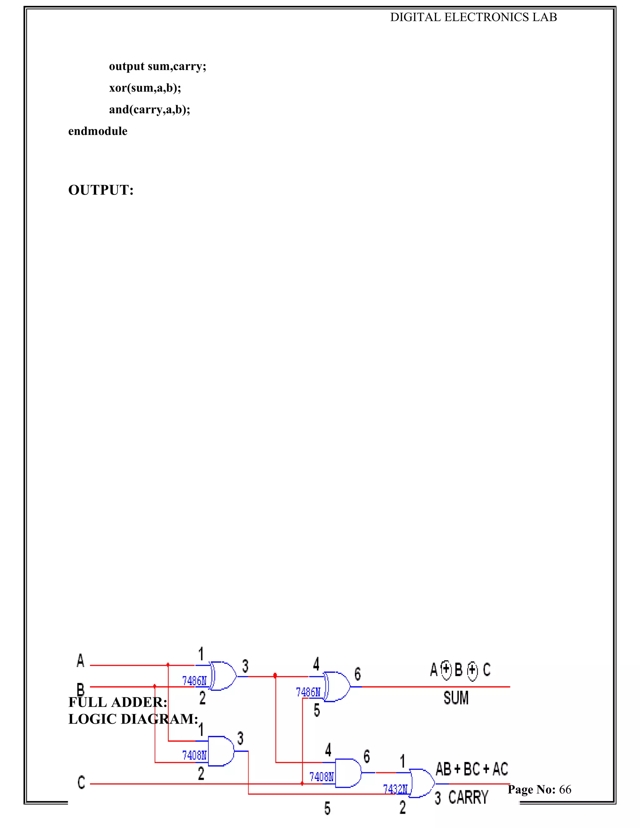
FULL ADDER:
A full adder is a combinational circuit that forms the arithmetic sum of three bits. It
consists of three inputs and two outputs. Two of the input variables, denoted by ‘a’
and ‘b’, represent the two significant bits to be added. The third input ‘c’ represents
the carry from the previous lower significant position. Two outputs are necessary
because the arithmetic sum of three binary digits ranges in value from 0 to 3, and
binary 2 or 3 needs two digits. The two outputs are designated by the symbols S for
sum and D for carry. The binary variable S gives the value of the least significant bit
of the sum. The binary variable D gives the output carry. The truth table of the full
adder is listed in table. The eight rows under the input variables designate all
possible combinations of the variables. The output variables are determined from the
arithmetic sum of the input bits. When all input bits are 0, the output is 0. The S
Page No: 64
62.
DIGITAL ELECTRONICS LAB
outputis equal to 1 when only one input is equal to 1 or when all three inputs are
equal to 1. The D output has a carry of 1 if two or three inputs are equal to 1.
The input and output bits of the combinational circuit different interpretations at
various stages of the problem. Physically, the binary signals of the inputs are
considered binary digits to be added arithmetically to form a two-digit sum at the
output. On the other hand, the same binary values are considered as variables of
Boolean functions when expressed in the truth table or when the circuit is
implemented with logic gates. The maps for the output of the full adder are shown in
below.
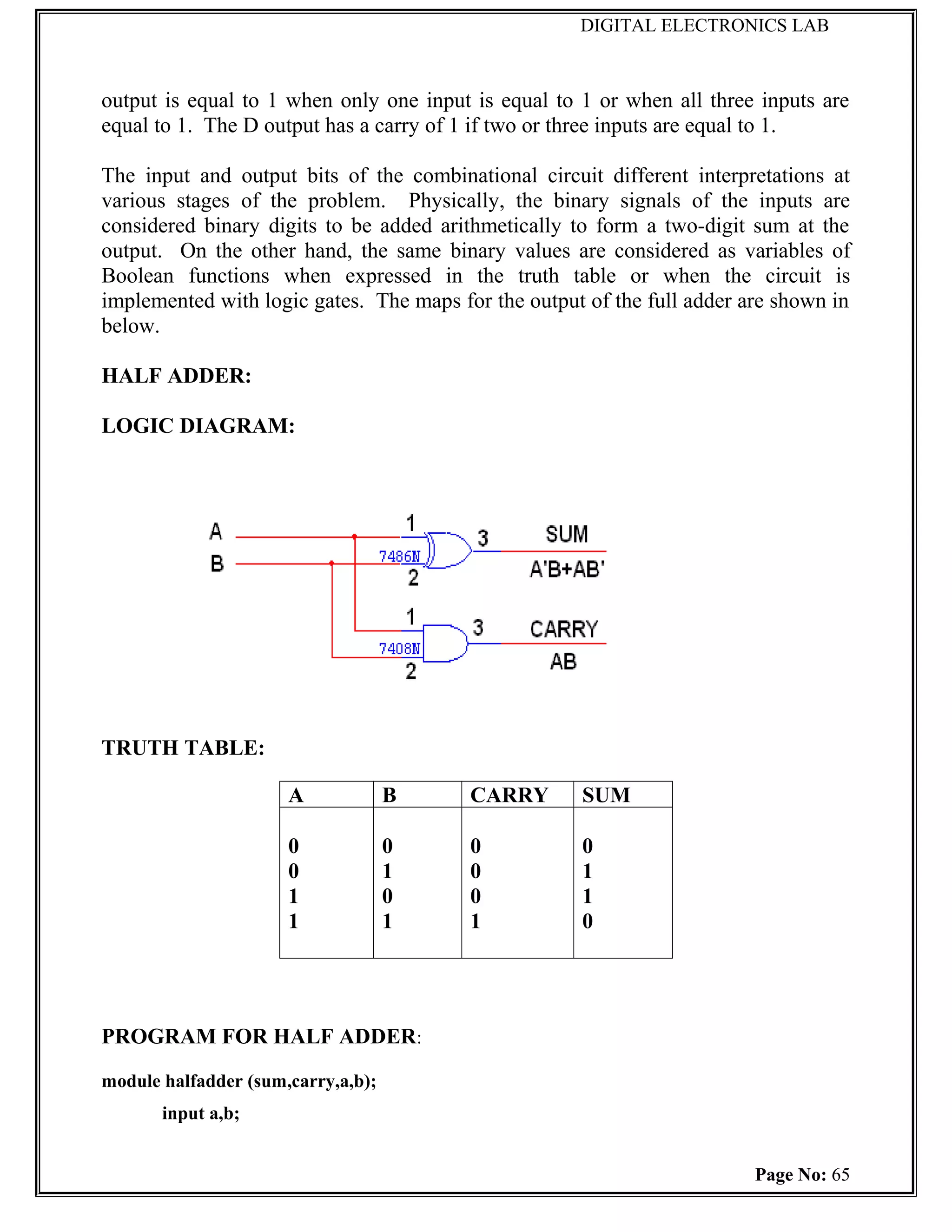
HALF ADDER:
LOGIC DIAGRAM:
TRUTH TABLE:
A B CARRY SUM
0 0 0 0
0 1 0 1
1 0 0 1
1 1 1 0
PROGRAM FOR HALF ADDER:
module halfadder (sum,carry,a,b);
input a,b;
Page No: 65
63.
DIGITAL ELECTRONICS LAB
output sum,carry;
xor(sum,a,b);
and(carry,a,b);
endmodule
OUTPUT:
FULL ADDER:
LOGIC DIAGRAM:
Page No: 66
64.
DIGITAL ELECTRONICS LAB
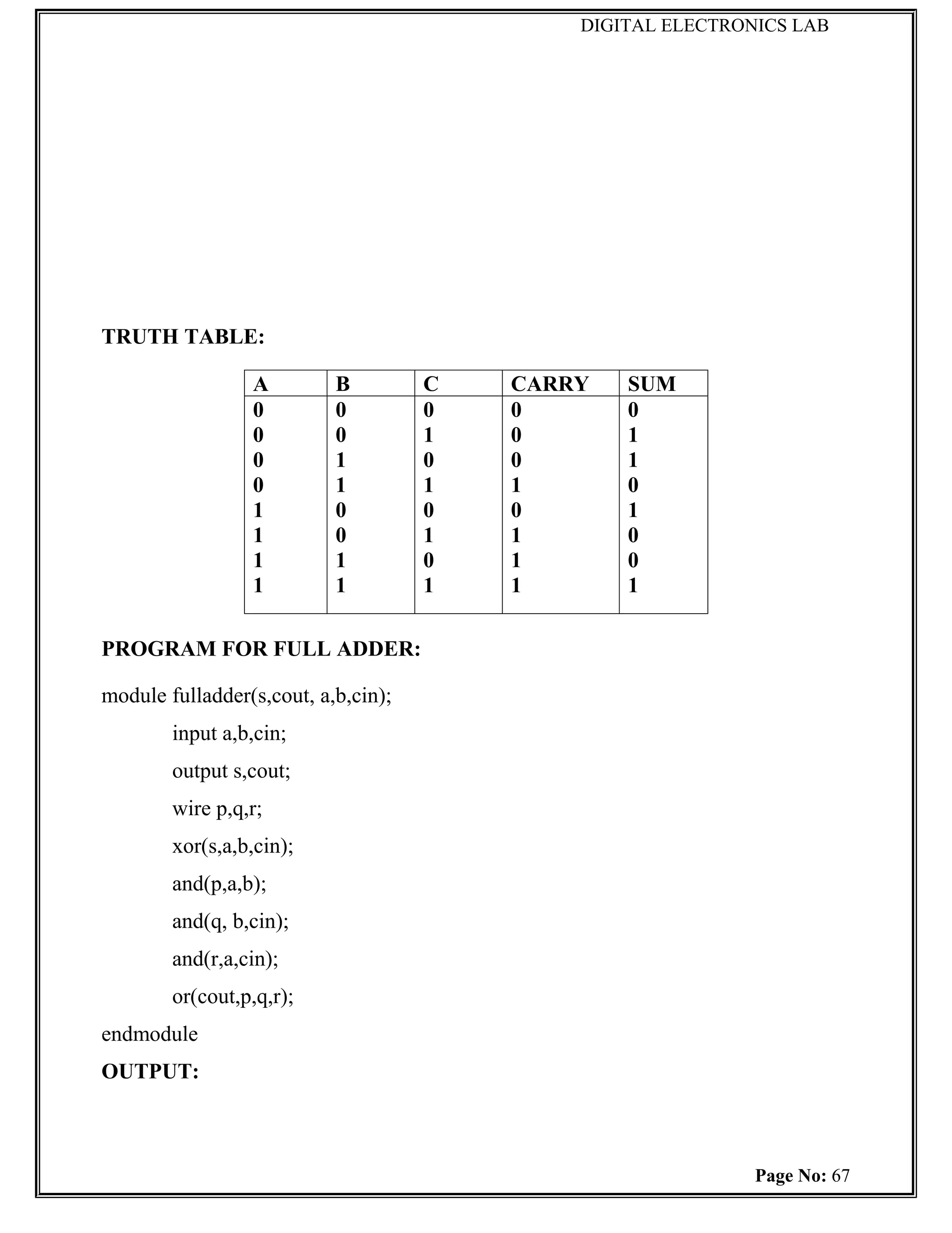
TRUTHTABLE:
A B C CARRY SUM
0 0 0 0 0
0 0 1 0 1
0 1 0 0 1
0 1 1 1 0
1 0 0 0 1
1 0 1 1 0
1 1 0 1 0
1 1 1 1 1
PROGRAM FOR FULL ADDER:
module fulladder(s,cout, a,b,cin);
input a,b,cin;
output s,cout;
wire p,q,r;
xor(s,a,b,cin);
and(p,a,b);
and(q, b,cin);
and(r,a,cin);
or(cout,p,q,r);
endmodule
OUTPUT:
Page No: 67
65.
DIGITAL ELECTRONICS LAB
HALFSUBTRACTOR:
LOGIC DIAGRAM:
TRUTH TABLE:
A B BORROW DIFFERENCE
0 0 0 0
0 1 1 1
1 0 0 1
1 1 0 0
PROGRAM FOR HALF SUBTRACTOR:
module halfsubtractor(diff,borrow, a,b);
Page No: 68
66.
DIGITAL ELECTRONICS LAB
input a,b;
output diff,borrow;
xor(diff,a,b);
not(a1,a)
and(borrow,a1,b);
endmodule
OUTPUT:
FULL SUBTRACTOR:
LOGIC DIAGRAM:
TRUTH TABLE:
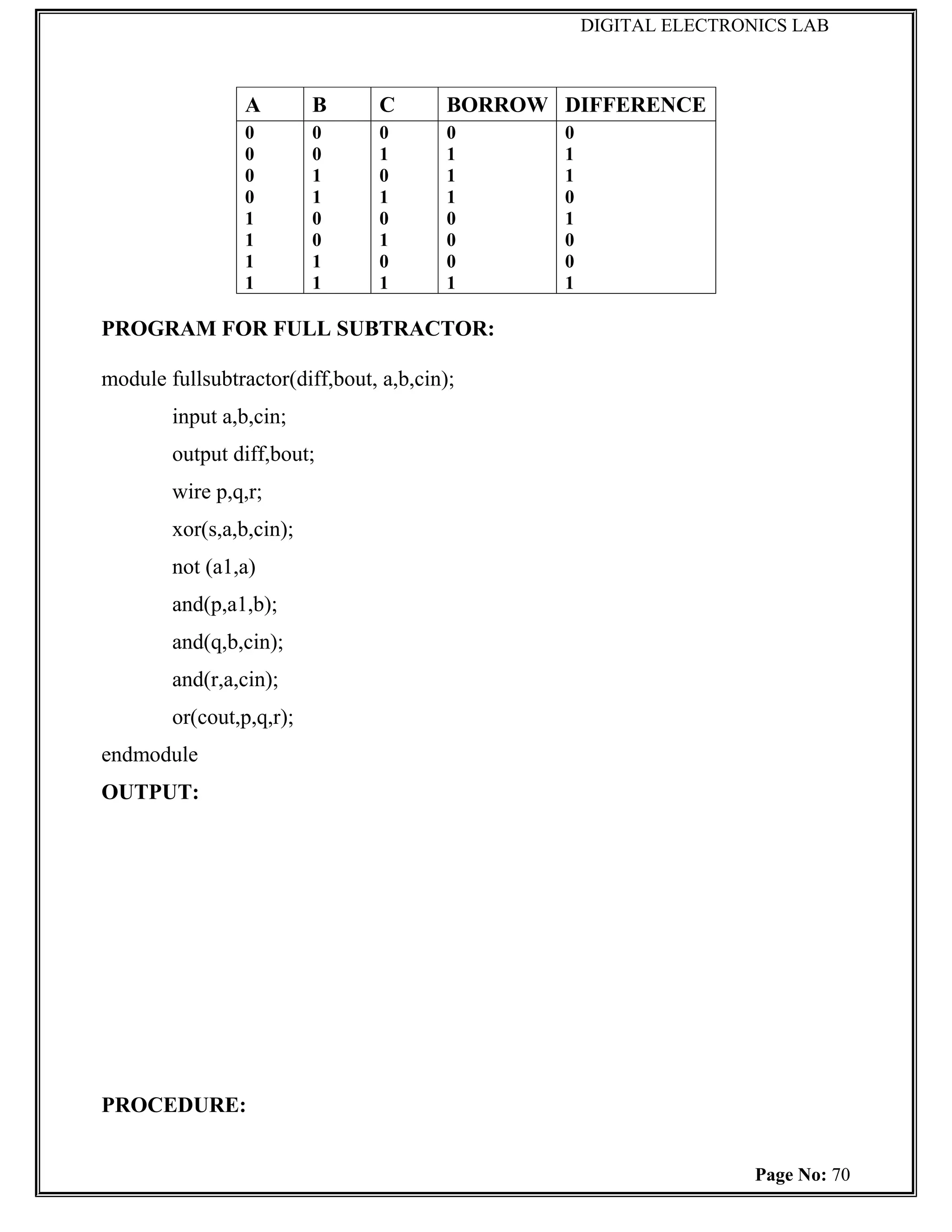
Page No: 69
67.
DIGITAL ELECTRONICS LAB
A B C BORROW DIFFERENCE
0 0 0 0 0
0 0 1 1 1
0 1 0 1 1
0 1 1 1 0
1 0 0 0 1
1 0 1 0 0
1 1 0 0 0
1 1 1 1 1
PROGRAM FOR FULL SUBTRACTOR:
module fullsubtractor(diff,bout, a,b,cin);
input a,b,cin;
output diff,bout;
wire p,q,r;
xor(s,a,b,cin);
not (a1,a)
and(p,a1,b);
and(q,b,cin);
and(r,a,cin);
or(cout,p,q,r);
endmodule
OUTPUT:
PROCEDURE:
Page No: 70
68.
DIGITAL ELECTRONICS LAB
Open project navigator.
Go to the file and click the new project
Type the project name
The “property wizard” is open to check all properties such as product,
categories, family, device etc. then click next
Create new source wizard appears then click next
Project summary is displayed then click next
Go to the project and click “new source”
Then type the module name as well as select verilog module then click next
“Define module window” here we assign the input and output of half adder,
clicks next and click finish
Type the program and save it
Make sure that the source is in “BEHAVIOURAL SIMULATION”
Then click the ISE simulator and view the signal window
Force the input data corresponding circuit
Simulate the program using ISE simulator
RESULT:
Thus the Verilog HDL program for adder and subtractor are written and
simulated using ISE simulator.
Page No: 71
69.
DIGITAL ELECTRONICS LAB
Ex.No: 13
SIMULATION OF MULTIPLEXER AND DE-MULTIPLEXER
Date: USING VERILOG HDL
AIM:
To write the Verilog HDL program for multiplexer and de-multiplexer circuit
and simulate it using ISE simulator.
HARDWARE& SOFTWARE REQUIRED:
XILINK 9.1i Simulator
PC WITH WINDOWS-XP
THEORY:
MULTIPLEXER:
A digital multiplexer is a combinational circuit that selects binary information
from one of many input lines and directs it to a single output line. The selection of a
particular input line is controlled by a set of selection lines. Normally, there are 2^n
inputs lines and n selection lines whose bit combinations determine which input is
selected.
In a 4 to 1 line multiplexer, the four input lines, I0 to I3 is applied to one input
of an AND gate. Selection lines S1 and S0 are decoded to select a particular AND
gate. A multiplexer is also called a data selector, since it selects one of many inputs
and steers the binary information to the output line.
DEMULTIPLEXER:
The demultiplexer does the reverse operation of a multiplexer. It can be used
to separate the multiplexed signal into individual signals, The select input code
determines to which output the data input will be transmitted. The number of output
lines is n and the number of select lines is m, where n=2^m. The input data is
transmitted to one of the output di by means of select signals a,b. The 4-bit adder
adds the input a & b and produces the 4-bit sum as the output.
Page No: 72
70.
DIGITAL ELECTRONICS LAB
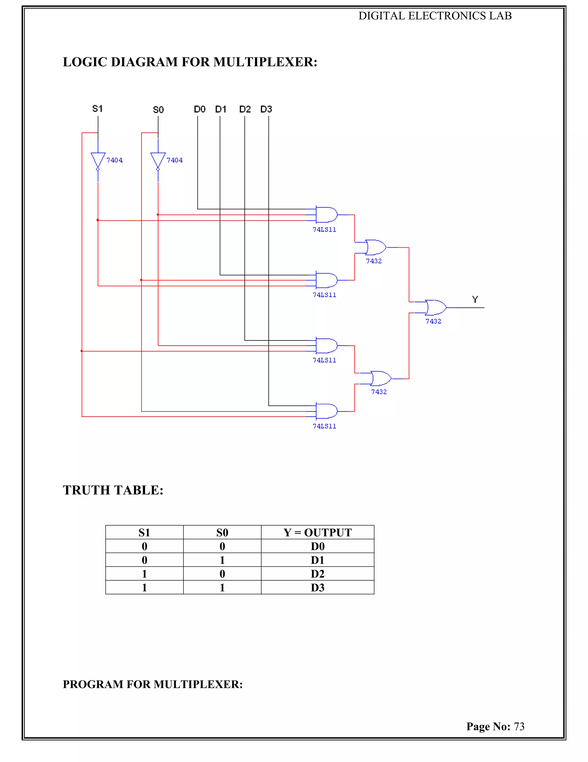
LOGICDIAGRAM FOR MULTIPLEXER:
TRUTH TABLE:
S1 S0 Y = OUTPUT
0 0 D0
0 1 D1
1 0 D2
1 1 D3
PROGRAM FOR MULTIPLEXER:
Page No: 73
71.
DIGITAL ELECTRONICS LAB
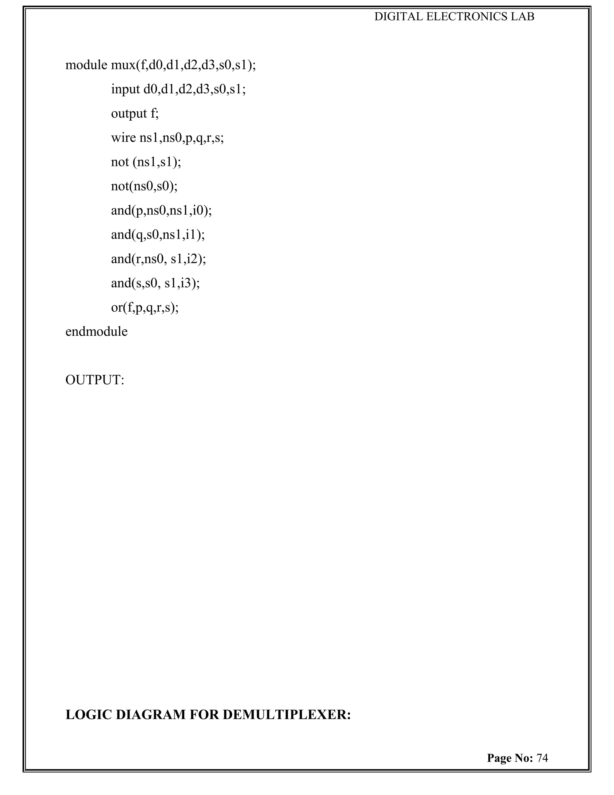
modulemux(f,d0,d1,d2,d3,s0,s1);
input d0,d1,d2,d3,s0,s1;
output f;
wire ns1,ns0,p,q,r,s;
not (ns1,s1);
not(ns0,s0);
and(p,ns0,ns1,i0);
and(q,s0,ns1,i1);
and(r,ns0, s1,i2);
and(s,s0, s1,i3);
or(f,p,q,r,s);
endmodule
OUTPUT:
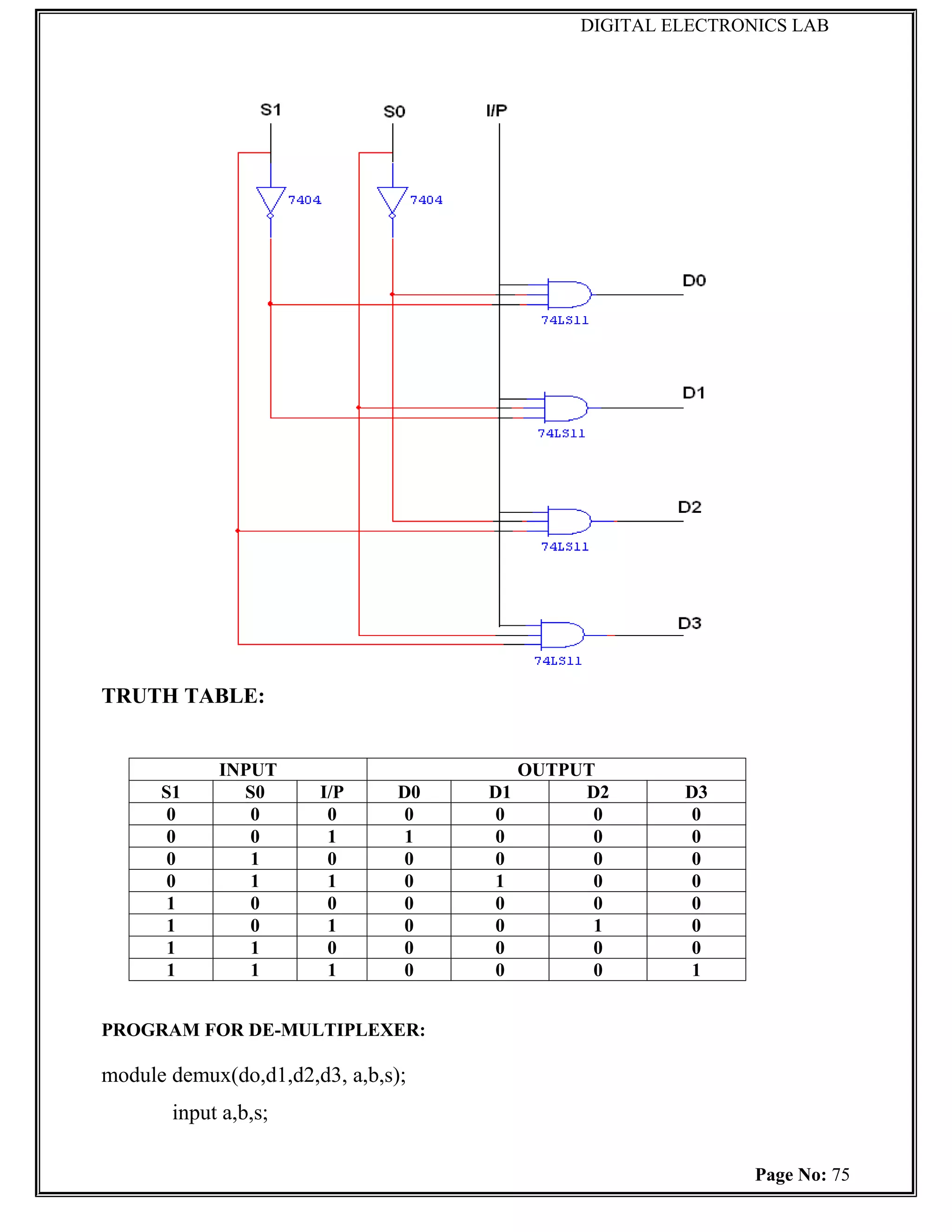
LOGIC DIAGRAM FOR DEMULTIPLEXER:
Page No: 74
DIGITAL ELECTRONICS LAB
output d0,d1,d2,d3;
wire a1,b1;
not (a1,a);
not(b1,b);
and(d0,b1,a1,s);
and(d1,b,a1,s);
and(d2,b1,a,s);
and(d3,b,a,s);
endmodule
OUTPUT:
PROCEDURE:
Open project navigator.
Go to the file and click the new project
Page No: 76
74.
DIGITAL ELECTRONICS LAB
Type the project name
The “property wizard” is open to check all properties such as product,
categories, family, device etc. then click next
Create new source wizard appears then click next
Project summary is displayed then click next
Go to the project and click “new source”
Then type the module name as well as select verilog module then click next
“Define module window” here we assign the input and output of half adder,
clicks next and click finish
Type the program and save it
Make sure that the source is in “BEHAVIOURAL SIMULATION”
Then click the ISE simulator and view the signal window
Force the input data corresponding circuit
Simulate the program using ISE simulator
RESULT:
Thus the Verilog HDL program for multiplexer and de-multiplexer are written
and simulated using ISE simulator.
Page No: 77


![Vibe Coding vs. Spec-Driven Development [Free Meetup]](https://cdn.slidesharecdn.com/ss_thumbnails/vibecodingvsspecdrivendevelopment-251209105622-43f455e7-thumbnail.jpg?width=640&height=640&fit=bounds)


