The document discusses CMOS inverters, NAND gates, and NOR gates. It describes the components and operation of each circuit. For CMOS inverters, it explains that one p-channel and one n-channel MOSFET are connected in series, with their gates connected as the input and drains as the output. A NAND gate uses two p-channel MOSFETs in parallel and two n-channel in series, while a NOR gate uses two p-channel in series and two n-channel in parallel. Truth tables are provided for each gate. Advantages of CMOS circuits include low power consumption and high noise immunity, while disadvantages are low switching speed and greater propagation delay.
This presentation has given a brief introduction and working of CMOS Logic Structures which includes MOS logic, CMOS logic, CMOS logic structure, CMOS complementary logic, pass transistor logic, bi CMOS logic, pseudo –nMOS logic, CMOS domino logic, Cascode Voltage Switch Logic(CVSL), clocked CMOS logic(c²mos), dynamic CMOS logic
This presentation discusses the basics about how to realize logic functions using Static CMOS logic. This presentation discusses about how to realize a Boolean expression by drawing a Pull-up network and a pull-down network. It also briefs about the pass transistor logic and the concepts of weak and strong outputs.
This document discusses the basics of pass transistor logic. It also discusses how to realize ta a boolean equation using PTL , advantages and limitations of pass transistor circuits
I have prepared it to create an understanding of delay modeling in VLSI.
Regards,
Vishal Sharma
Doctoral Research Scholar,
IIT Indore
vishalfzd@gmail.com
This presentation discusses the basics of Pass Transistor Logic, its advantages, limitation and finally implementation of Boolean functions/Combinational Logic circuits using Pass Transistor Logic.
The metal–oxide–semiconductor field-effect transistor (MOSFET, MOS-FET, or MOS FET) is a type of field-effect transistor (FET). It has an insulated gate, whose voltage determines the conductivity of the device. This ability to change conductivity with the amount of applied voltage can be used for amplifying or switching electronic signals. Although FET is sometimes used when referring to MOSFET devices, other types of field-effect transistors also exist.
A simple N-channel MOSFET can be used as a diode, Switch and Active resistor. This presentation is a part of course of Analog CMOS Design, based on textbook of same title by Allen Holberg.
DIFFERENTIAL AMPLIFIER using MOSFET, Modes of operation,
The MOS differential pair with a common-mode input voltage ,Common mode rejection,gain, advantages and disadvantages.
CMOS differential pairs are used for finding the difference between two voltage signal.But if not properly implemented then it will also cause amplification of common voltage.As well as to work as differential pair voltage should also be in proper range so that it should operate in steady state i.e. as amplifier.
CFD Simulation of By-pass Flow in a HRSG module by R&R Consult.pptxR&R Consult
CFD analysis is incredibly effective at solving mysteries and improving the performance of complex systems!
Here's a great example: At a large natural gas-fired power plant, where they use waste heat to generate steam and energy, they were puzzled that their boiler wasn't producing as much steam as expected.
R&R and Tetra Engineering Group Inc. were asked to solve the issue with reduced steam production.
An inspection had shown that a significant amount of hot flue gas was bypassing the boiler tubes, where the heat was supposed to be transferred.
R&R Consult conducted a CFD analysis, which revealed that 6.3% of the flue gas was bypassing the boiler tubes without transferring heat. The analysis also showed that the flue gas was instead being directed along the sides of the boiler and between the modules that were supposed to capture the heat. This was the cause of the reduced performance.
Based on our results, Tetra Engineering installed covering plates to reduce the bypass flow. This improved the boiler's performance and increased electricity production.
It is always satisfying when we can help solve complex challenges like this. Do your systems also need a check-up or optimization? Give us a call!
Work done in cooperation with James Malloy and David Moelling from Tetra Engineering.
More examples of our work https://www.r-r-consult.dk/en/cases-en/
Democratizing Fuzzing at Scale by Abhishek Aryaabh.arya
Presented at NUS: Fuzzing and Software Security Summer School 2024
This keynote talks about the democratization of fuzzing at scale, highlighting the collaboration between open source communities, academia, and industry to advance the field of fuzzing. It delves into the history of fuzzing, the development of scalable fuzzing platforms, and the empowerment of community-driven research. The talk will further discuss recent advancements leveraging AI/ML and offer insights into the future evolution of the fuzzing landscape.
Welcome to WIPAC Monthly the magazine brought to you by the LinkedIn Group Water Industry Process Automation & Control.
In this month's edition, along with this month's industry news to celebrate the 13 years since the group was created we have articles including
A case study of the used of Advanced Process Control at the Wastewater Treatment works at Lleida in Spain
A look back on an article on smart wastewater networks in order to see how the industry has measured up in the interim around the adoption of Digital Transformation in the Water Industry.
TECHNICAL TRAINING MANUAL GENERAL FAMILIARIZATION COURSEDuvanRamosGarzon1
AIRCRAFT GENERAL
The Single Aisle is the most advanced family aircraft in service today, with fly-by-wire flight controls.
The A318, A319, A320 and A321 are twin-engine subsonic medium range aircraft.
The family offers a choice of engines
Automobile Management System Project Report.pdfKamal Acharya
The proposed project is developed to manage the automobile in the automobile dealer company. The main module in this project is login, automobile management, customer management, sales, complaints and reports. The first module is the login. The automobile showroom owner should login to the project for usage. The username and password are verified and if it is correct, next form opens. If the username and password are not correct, it shows the error message.
When a customer search for a automobile, if the automobile is available, they will be taken to a page that shows the details of the automobile including automobile name, automobile ID, quantity, price etc. “Automobile Management System” is useful for maintaining automobiles, customers effectively and hence helps for establishing good relation between customer and automobile organization. It contains various customized modules for effectively maintaining automobiles and stock information accurately and safely.
When the automobile is sold to the customer, stock will be reduced automatically. When a new purchase is made, stock will be increased automatically. While selecting automobiles for sale, the proposed software will automatically check for total number of available stock of that particular item, if the total stock of that particular item is less than 5, software will notify the user to purchase the particular item.
Also when the user tries to sale items which are not in stock, the system will prompt the user that the stock is not enough. Customers of this system can search for a automobile; can purchase a automobile easily by selecting fast. On the other hand the stock of automobiles can be maintained perfectly by the automobile shop manager overcoming the drawbacks of existing system.
Cosmetic shop management system project report.pdfKamal Acharya
Buying new cosmetic products is difficult. It can even be scary for those who have sensitive skin and are prone to skin trouble. The information needed to alleviate this problem is on the back of each product, but it's thought to interpret those ingredient lists unless you have a background in chemistry.
Instead of buying and hoping for the best, we can use data science to help us predict which products may be good fits for us. It includes various function programs to do the above mentioned tasks.
Data file handling has been effectively used in the program.
The automated cosmetic shop management system should deal with the automation of general workflow and administration process of the shop. The main processes of the system focus on customer's request where the system is able to search the most appropriate products and deliver it to the customers. It should help the employees to quickly identify the list of cosmetic product that have reached the minimum quantity and also keep a track of expired date for each cosmetic product. It should help the employees to find the rack number in which the product is placed.It is also Faster and more efficient way.
Overview of the fundamental roles in Hydropower generation and the components involved in wider Electrical Engineering.
This paper presents the design and construction of hydroelectric dams from the hydrologist’s survey of the valley before construction, all aspects and involved disciplines, fluid dynamics, structural engineering, generation and mains frequency regulation to the very transmission of power through the network in the United Kingdom.
Author: Robbie Edward Sayers
Collaborators and co editors: Charlie Sims and Connor Healey.
(C) 2024 Robbie E. Sayers
Courier management system project report.pdfKamal Acharya
It is now-a-days very important for the people to send or receive articles like imported furniture, electronic items, gifts, business goods and the like. People depend vastly on different transport systems which mostly use the manual way of receiving and delivering the articles. There is no way to track the articles till they are received and there is no way to let the customer know what happened in transit, once he booked some articles. In such a situation, we need a system which completely computerizes the cargo activities including time to time tracking of the articles sent. This need is fulfilled by Courier Management System software which is online software for the cargo management people that enables them to receive the goods from a source and send them to a required destination and track their status from time to time.
Water scarcity is the lack of fresh water resources to meet the standard water demand. There are two type of water scarcity. One is physical. The other is economic water scarcity.
Forklift Classes Overview by Intella PartsIntella Parts
Discover the different forklift classes and their specific applications. Learn how to choose the right forklift for your needs to ensure safety, efficiency, and compliance in your operations.
For more technical information, visit our website https://intellaparts.com
Halogenation process of chemical process industries
Cmos logic
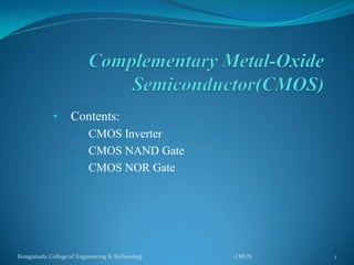
1. • Contents:
CMOS Inverter
CMOS NAND Gate
CMOS NOR Gate
Kongunadu College of Engineering & Technology CMOS 1
2. CMOS Inverter
It consists of two MOSFETs in series in such a way that a p-
channel device has its source connected to +VDD(a positive
voltage) and the n-channel has its source connected to ground.
The gates of the two devices connected together as the
common input and the drains are connected together as the
common output.
When input is HIGH, the gate of Q1(p-channel) is at 0 V
relative to the source of Q1 i.e. Vgs1=0 V. Thus Q1 is OFF. On
the other hand, the gate of Q2(n-channel) is at +VDD relative to
its source i.e. Vgs2=+VDD. Thus Q2 is ON. This will produce
VOUT=0 V.
When input is LOW, the gate of Q1(p-channel) is at negative
potential relative to its source while Q2 has Vgs=0 V.Thus,Q1 is
ON and Q2 is OFF. This produces output voltage approximately
+VDD.
Kongunadu College of Engineering & Technology CMOS 2
3. A Q1 Q2 Output
0 ON OFF 1
1 OFF ON 0
Truth Table
Kongunadu College of Engineering & Technology CMOS 3
4. Contd…
Different symbols used for the p-channel and n-
channel transistors to reflect their logical behaviour.
The n-channel transistor (Q2) is switched ‘ON’ when a
HIGH voltage is applied at the input.
The p-channel transistor (Q1) has the opposite
behaviour, it is switched ON when a LOW voltage is
applied at the input.
It is indicated by placing bubble in the symbol
Kongunadu College of Engineering & Technology CMOS 4
5. CMOS NAND Gate
It consists of two p-channel MOSFETs,Q1 and
Q2,connected in parallel and two n-channel MOSFETs,Q3
and Q4 are connected in series.
When Q1 and Q2 are both ON. Since the gate-to-source
voltages of Q3 and Q4(n-channel MOSFETs) are both 0 V,
those MOSFETs are OFF.
The output is therefore connected to +VDD(HIGH)
through Q1 and Q2 and is disconnected from ground and
the equivalent switching circuit when A=0 and B=+VDD.
In this case,Q1 is on because VGS1=-VDD and Q4 is ON
because VGS4=+VDD.
MOSFETs Q2 and Q3 are off because gate-to-source
voltages are 0 V.
Kongunadu College of Engineering & Technology CMOS 5
6. Contd…
Since Q1 is ON and Q3 is OFF, the output is connected to
+VDD and it is connected from ground.
When A=+VDD and B=0 V, the situation is similar(not
shown);the output is connected to +VDD through Q2 and
it is disconnected from ground because Q4 is OFF.
Finally, when both inputs are high(A=B=+VDD),
MOSFTETs Q1 and Q2 are both OFF and Q3 and Q4 are
both ON.
Thus, the output is connected to the ground through Q3
and Q4 and it is disconnected from +VDD.
Kongunadu College of Engineering & Technology CMOS 6
8. A B Q1 Q2 Q3 Q4 Output
0 0 ON ON OFF OFF 1
0 1 ON OFF OFF ON 1
1 0 OFF ON ON OFF 1
1 1 OFF OFF ON ON 0
Truth Table of NAND Gate
Kongunadu College of Engineering & Technology CMOS 8
9. CMOS NOR Gate
Here, p-channel MOSFETs Q1 and Q2 are connected in
series and n-channel MOSFETs Q3 and Q4 are connected
in parallel.
Like NAND circuit, this circuit can be analysed by
realizing that a LOW at any input turns ON its
corresponding p-channel MOSFET and turns OFF its
corresponding n-channel MOSFET and vice versa for a
HIGH input.
Kongunadu College of Engineering & Technology CMOS 9
11. Truth Table of NOR Gate
Kongunadu College of Engineering & Technology CMOS 11
12. Advantages
Consumes less power.
Can be operated at high voltages, resulting in improved
noise immunity.
Fan-out is more.
Better noise margin.
Disadvantages
Susceptible to static charge.
Switching speed low
Greater propagation delay
Kongunadu College of Engineering & Technology CMOS 12
13. Conclusion
The CMOS circuit is discussed for mode of operations such as
inverter, NAND and NOR gates.
References:
Mandal, “Digital Electronics Principles & Application,
McGraw Hill Edu, 2013.
William Keitz, Digital Electronics-A Practical Approach with
VHDL, Pearson, 2013.
Thomas L.Floyd, ‘Digital Fundamentals’, 11th edition, Pearson
Education, 2015.
Charles H.Roth, Jr, Lizy Lizy Kurian John, ‘Digital System
Design using VHDL, Cengage,2013.
D.P.Kothari,J.S.Dhillon, ‘Digital circuits and Design’,Pearson
Education, 2016.
A.P.Godse., Dr.D.A.Godse, ‘Digital Logic Circuits’ , Technical
Publications Third Edition 2016
Other Web Sources
Kongunadu College of Engineering & Technology CMOS 13