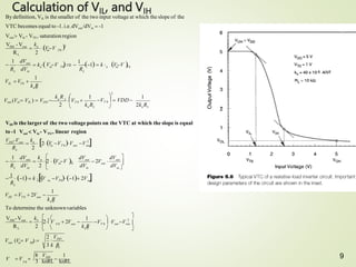
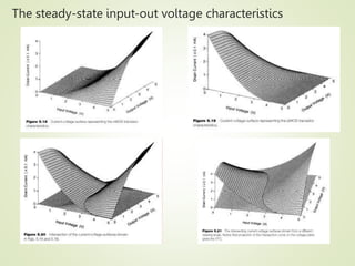
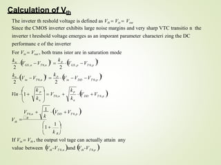
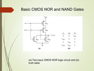
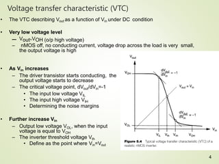
1. The document discusses the static characteristics of MOS inverters, including their voltage transfer characteristic (VTC). The VTC describes the output voltage (Vout) as a function of the input voltage (Vin) under DC conditions.
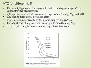
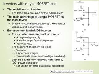
2. Key parameters that determine the VTC include the threshold voltage of the driver transistor (VT0), the product of kn and the load resistance (knRL), and the power supply voltage (VDD). Larger knRL results in a steeper transition slope and smaller output low voltage (VOL).
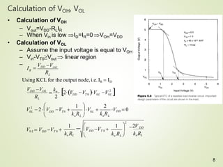
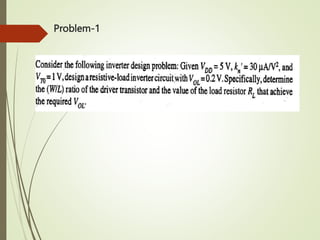
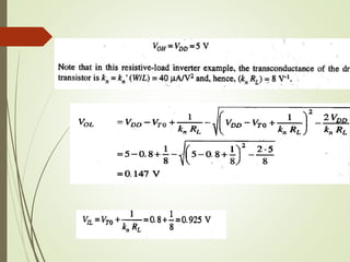
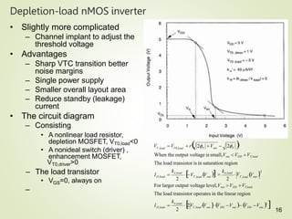
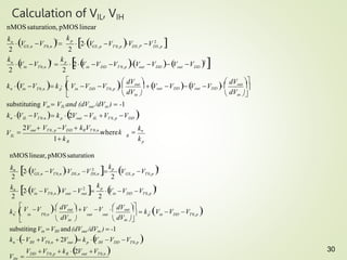
3. Calculations are shown for determining the output high (VOH) and low (VOL) voltages, as well as the input voltages (VIL,
![6
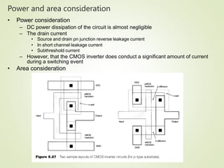
Power and area consideration
• The DC power dissipation
– The product of its power supply voltage and the amount of current
down from the power supply during steady state or in standby mode
– PDC=VDDIDC=(VDD/2)[IDC(Vin=low)+IDC(Vin=high)]
– In deep submicron technologies
• Subthreshold current more power consumption
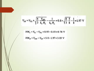
• The chip area
– To reduce the area of the MOS transistor
• The gate area of the MOS transistor
• The product of W and L](https://image.slidesharecdn.com/cmosinverterstaticcharacterstics-230422112002-0c5c9eda/85/CMOS-Inverter-static-characterstics-pptx-6-320.jpg)