The document is about CMOS logic design. It covers topics such as logic values and encoding bits in digital systems, logic gates and families, MOS transistors, CMOS inverters and their electrical characteristics. It discusses power consumption analysis of CMOS circuits including static and dynamic power. It also covers pull-up and pull-down networks, DC analysis of CMOS inverters, beta ratio, switching characteristics of inverters and examples of CMOS logic gates like inverters, NAND, NOR, buffers and AND/OR gates.
Mr. S. M.Karve
Department of Electronics & Telecommunication
Engineering
VLSI Design
Unit No. 5
CMOS Logic Design
Prepared By
2.
Logic Values
Encoder bits
Logic Gates
Logic Families
MOS Transistors
CMOS Inverter
CMOS Electrical Characteristics
Power Consumption Analysis of CMOS Circuits
Pull-up and Pull-Down Network
DC Analysis/Characteristics of CMOS Inverter
Beta Ratio
Switching Characteristics of CMOS Inverter
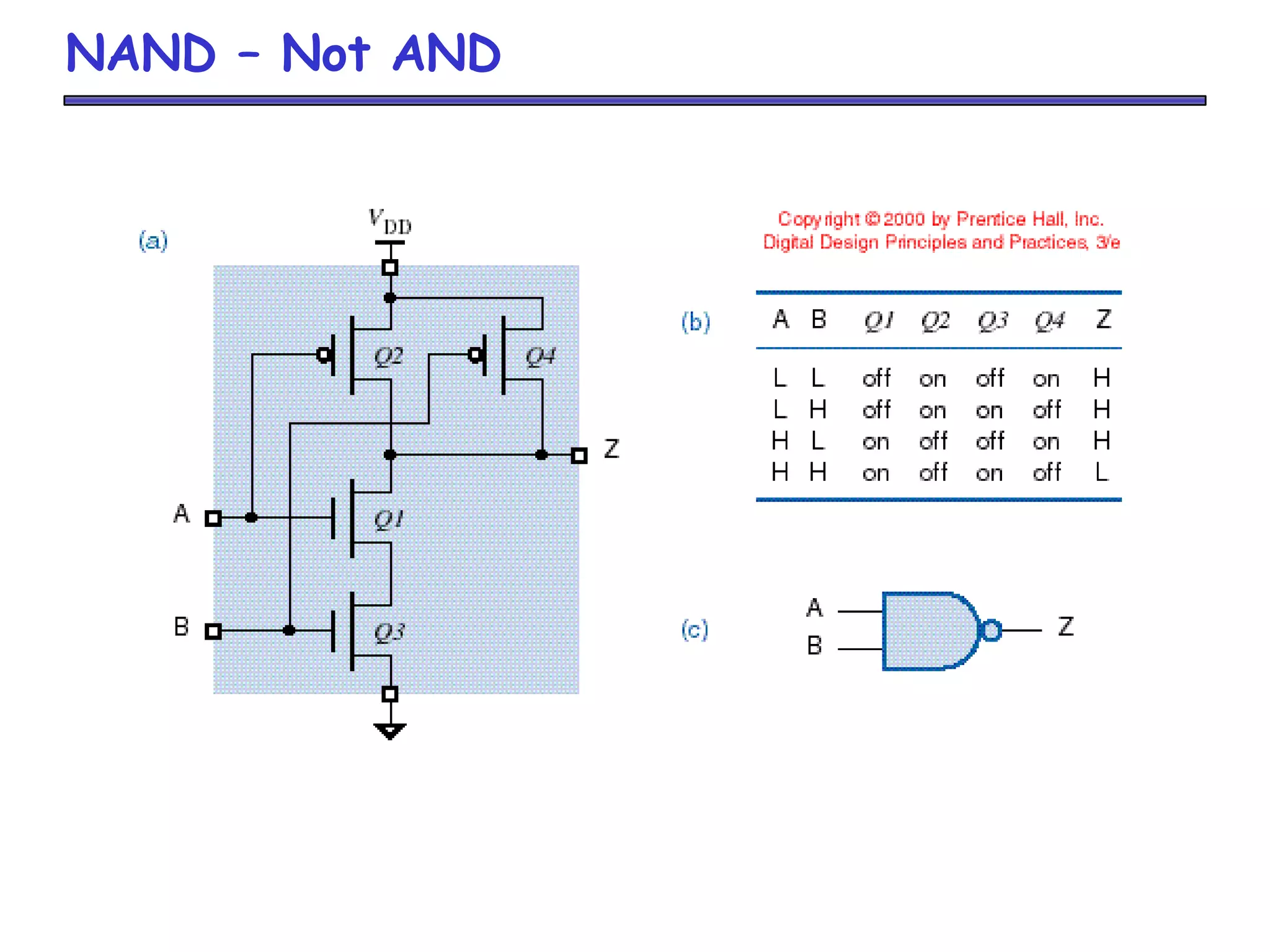
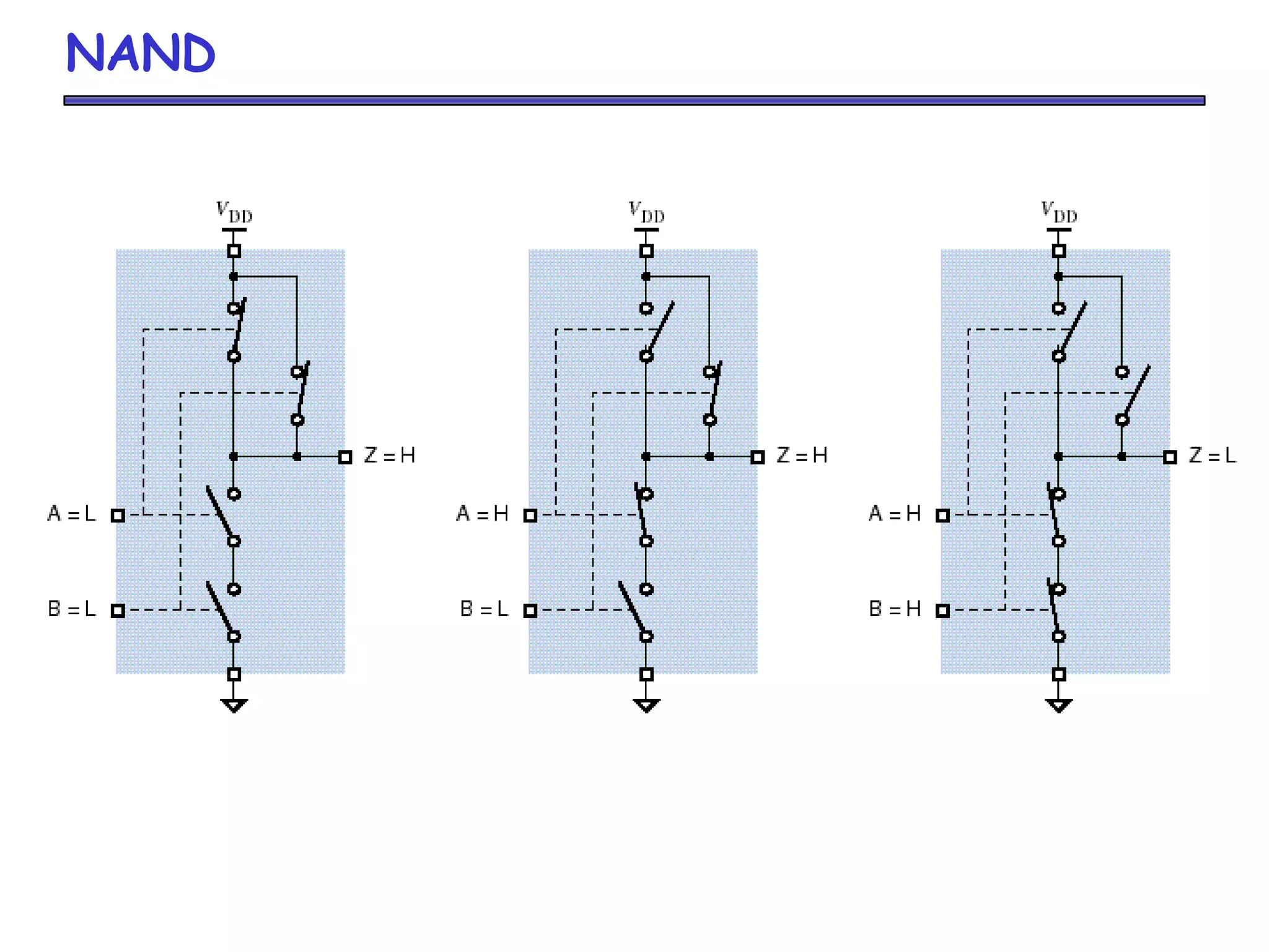
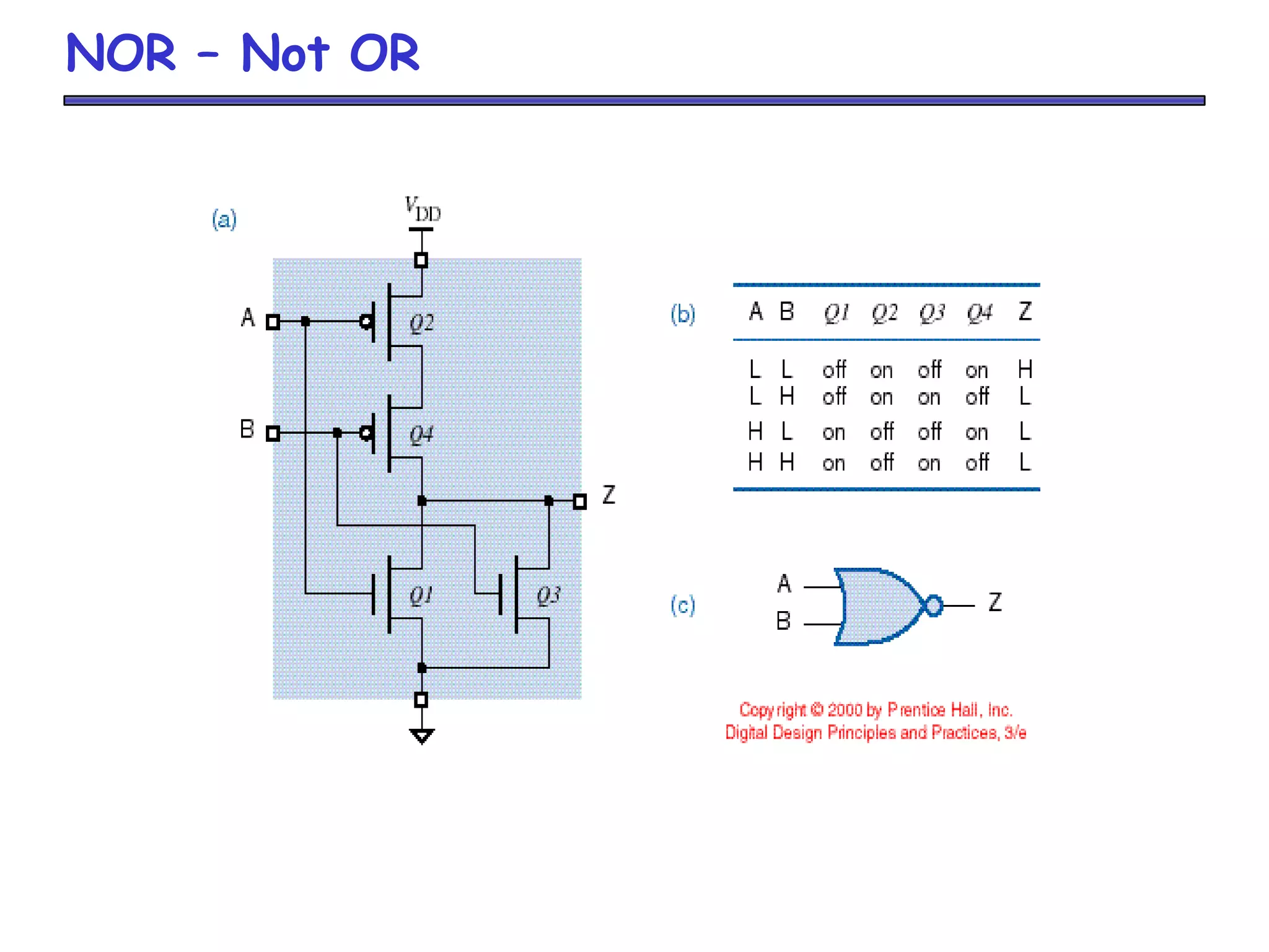
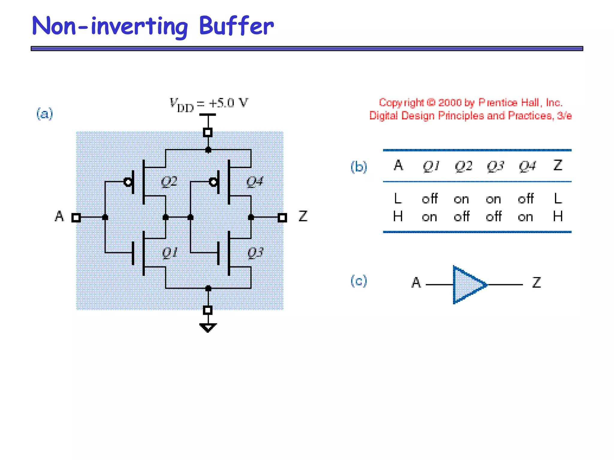
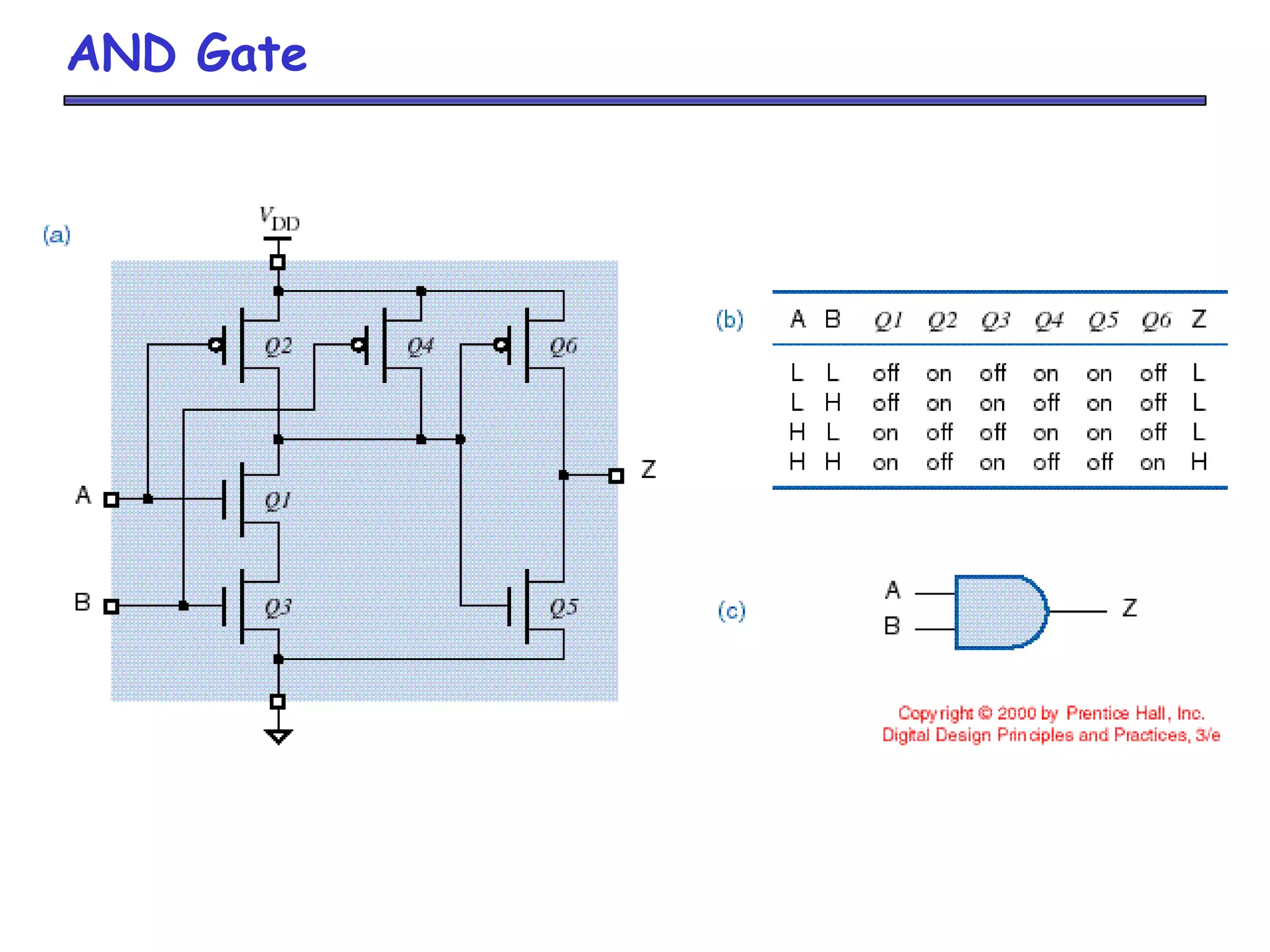
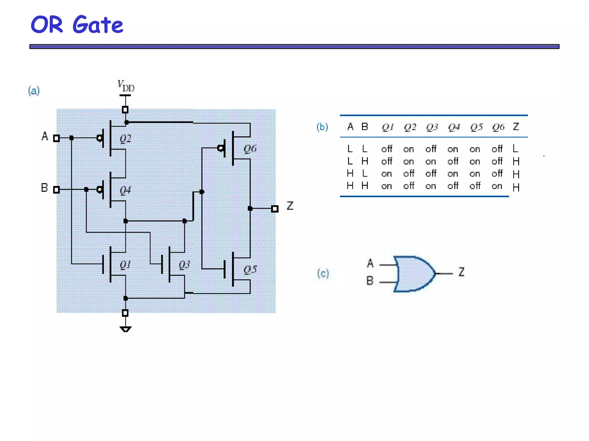
CMOS logic gates and its Examples
Implementation of Boolean equations using CMOS Logic
Contents
3.
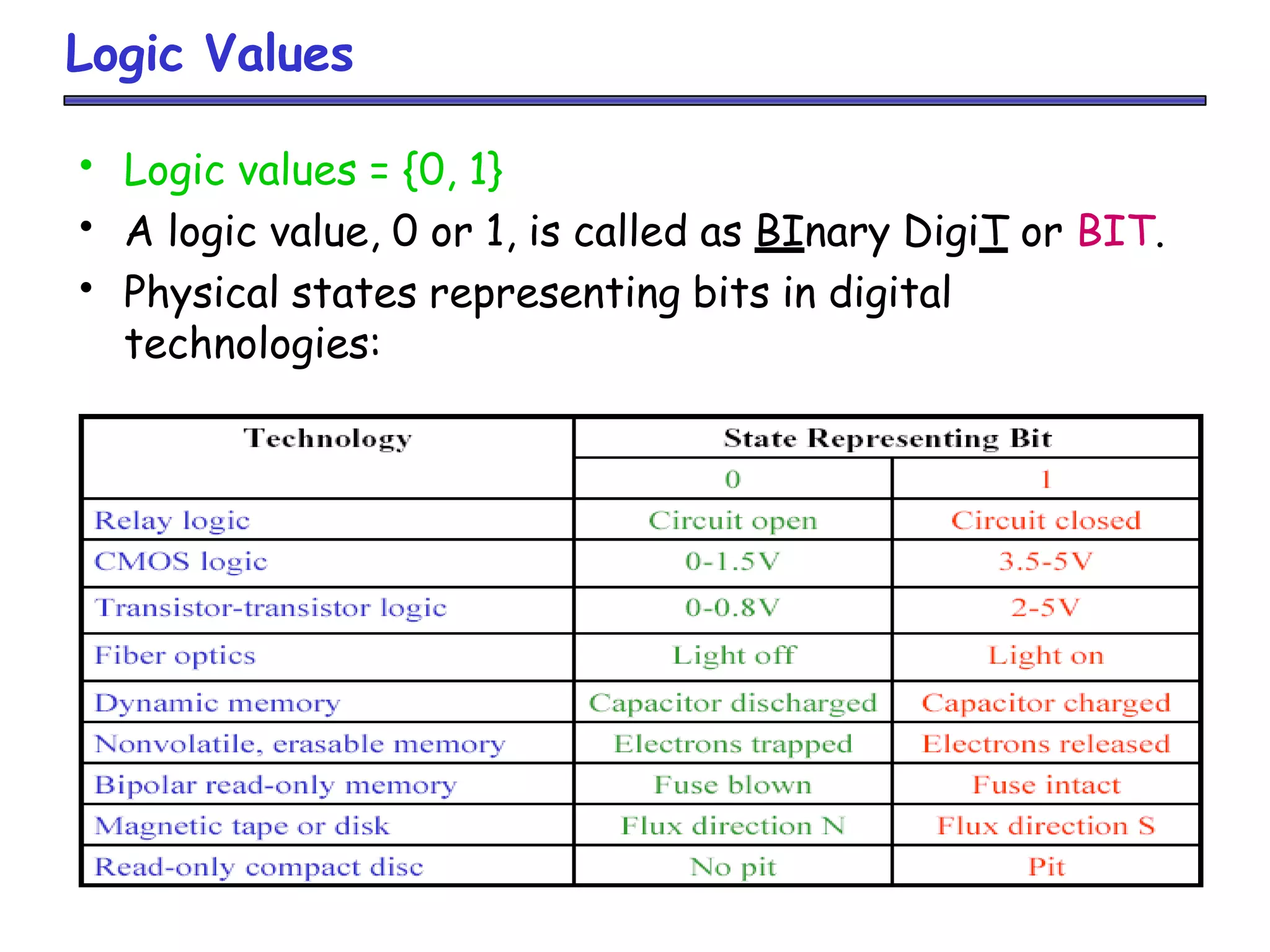
Logic Values
• Logicvalues = {0, 1}
• A logic value, 0 or 1, is called as BInary DigiT or BIT.
• Physical states representing bits in digital
technologies:
4.
Encoding Bits
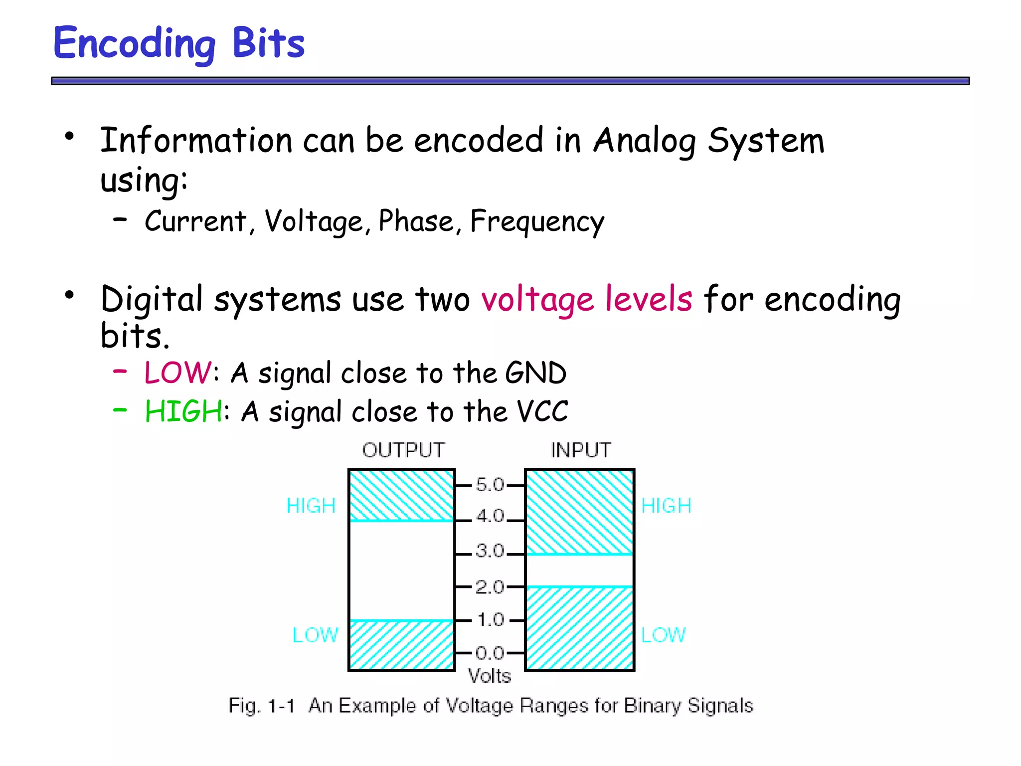
• Informationcan be encoded in Analog System
using:
– Current, Voltage, Phase, Frequency
• Digital systems use two voltage levels for encoding
bits.
– LOW: A signal close to the GND
– HIGH: A signal close to the VCC
5.
Encoding Bits
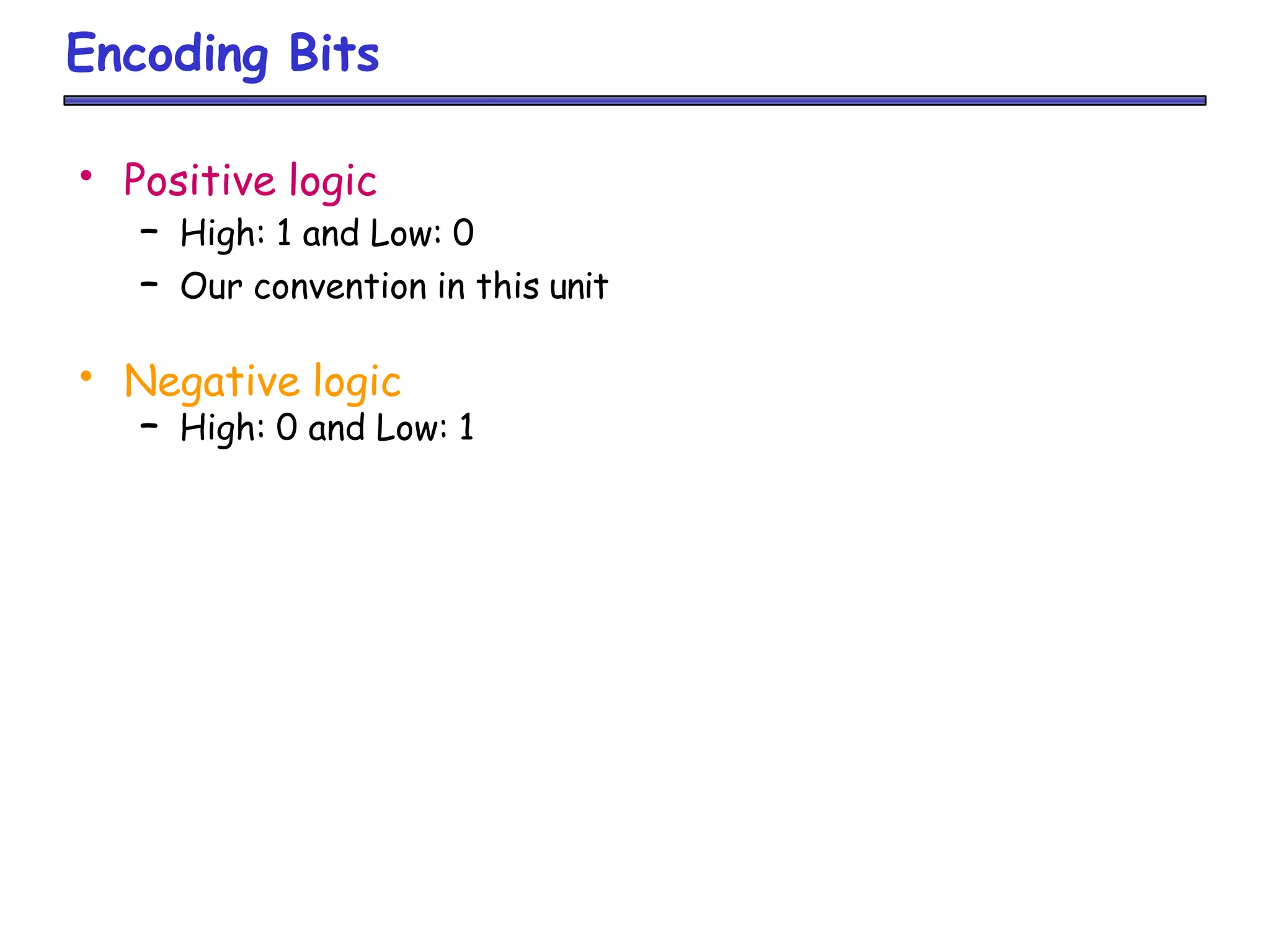
• Positivelogic
– High: 1 and Low: 0
– Our convention in this unit
• Negative logic
– High: 0 and Low: 1
6.
Logic Gates
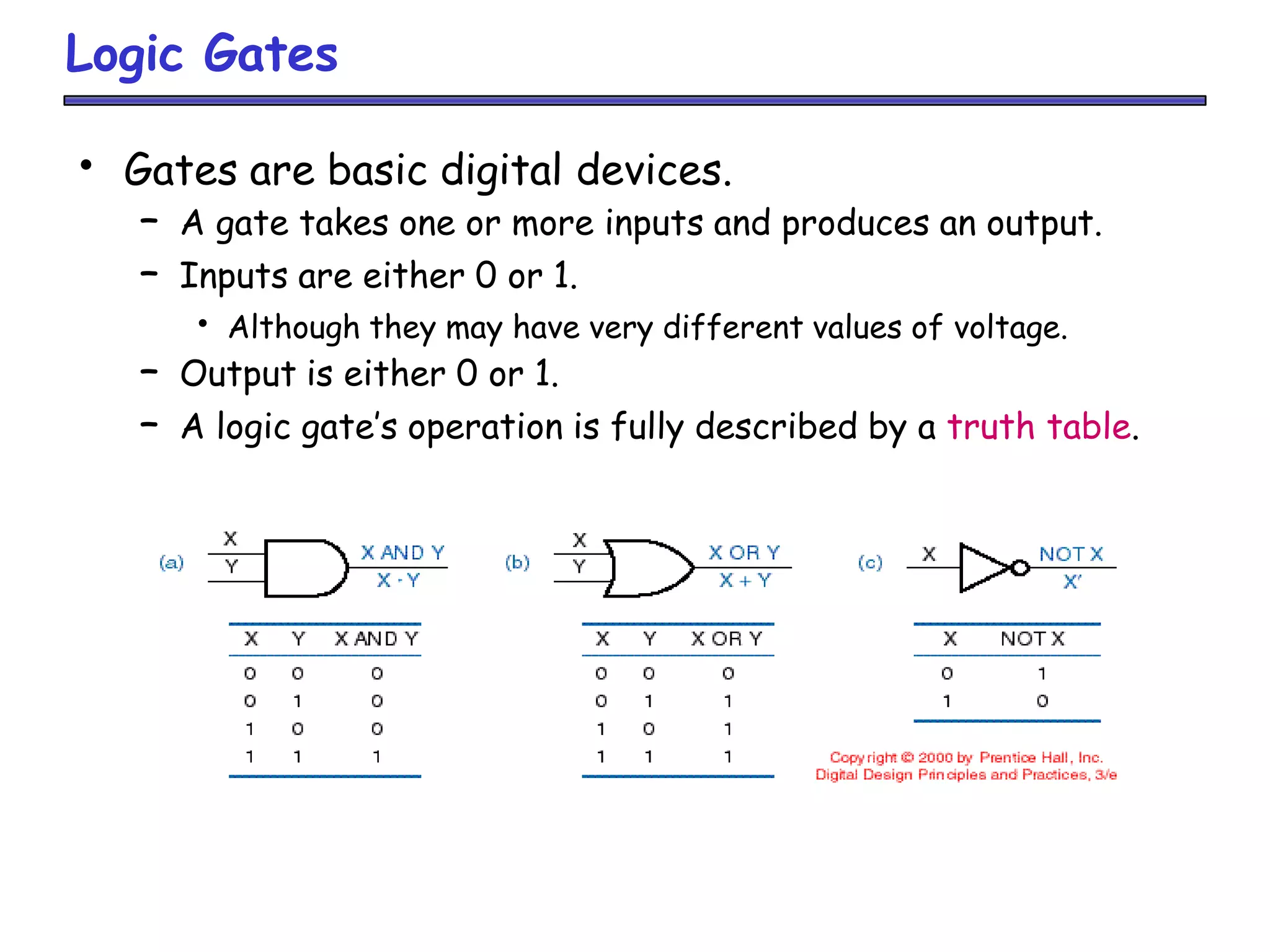
• Gatesare basic digital devices.
– A gate takes one or more inputs and produces an output.
– Inputs are either 0 or 1.
• Although they may have very different values of voltage.
– Output is either 0 or 1.
– A logic gate’s operation is fully described by a truth table.
7.
Logic Families –What is inside of a logic gate?
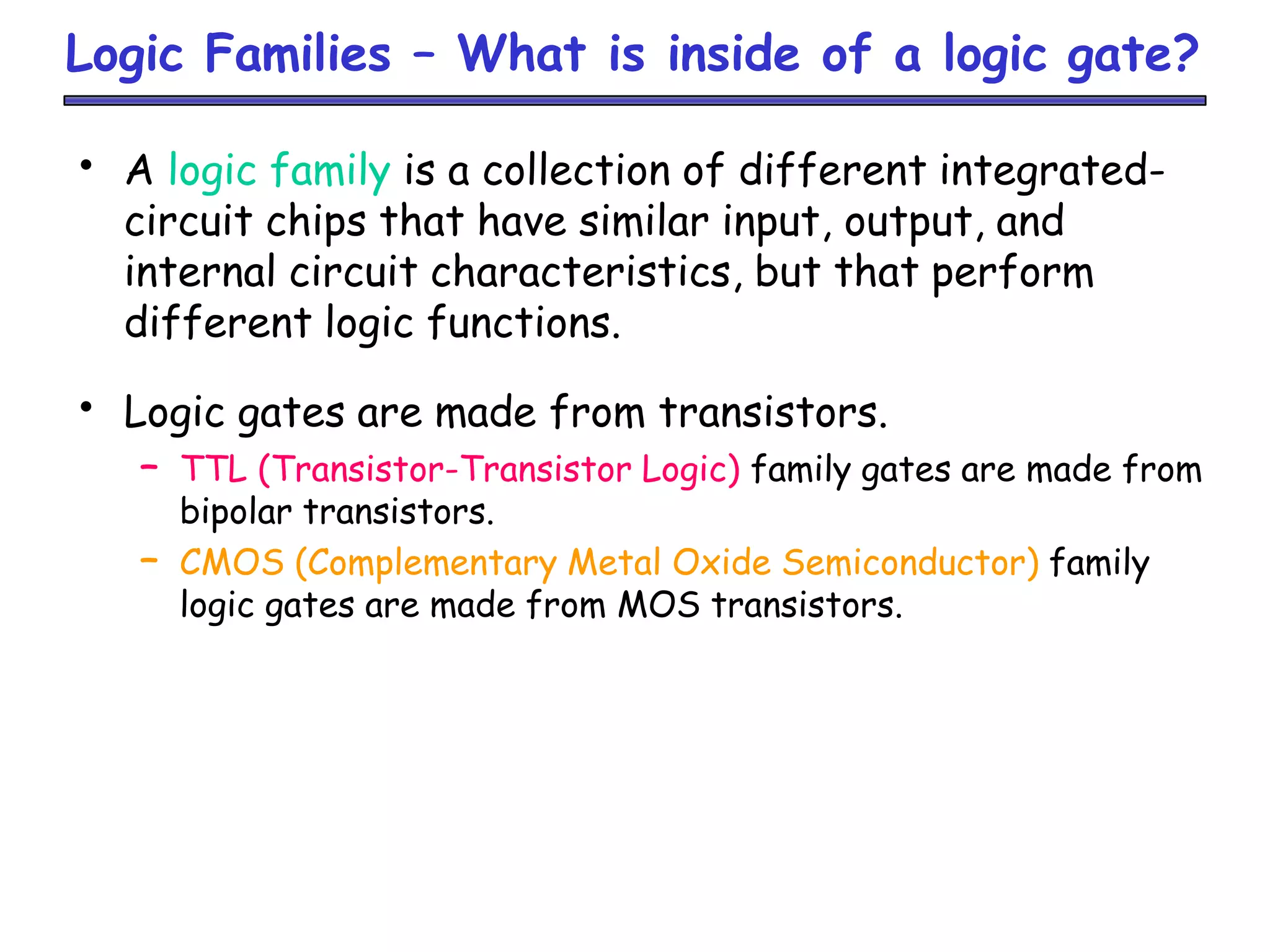
• A logic family is a collection of different integrated-
circuit chips that have similar input, output, and
internal circuit characteristics, but that perform
different logic functions.
• Logic gates are made from transistors.
– TTL (Transistor-Transistor Logic) family gates are made from
bipolar transistors.
– CMOS (Complementary Metal Oxide Semiconductor) family
logic gates are made from MOS transistors.
8.
MOS Transistors –N-type MOSFET
• OFF (open circuit) : when gate is logical zero
• ON (short circuit) : when gate is logical one
•
•
Passes a good logical zero
Degrades a logical one
9.
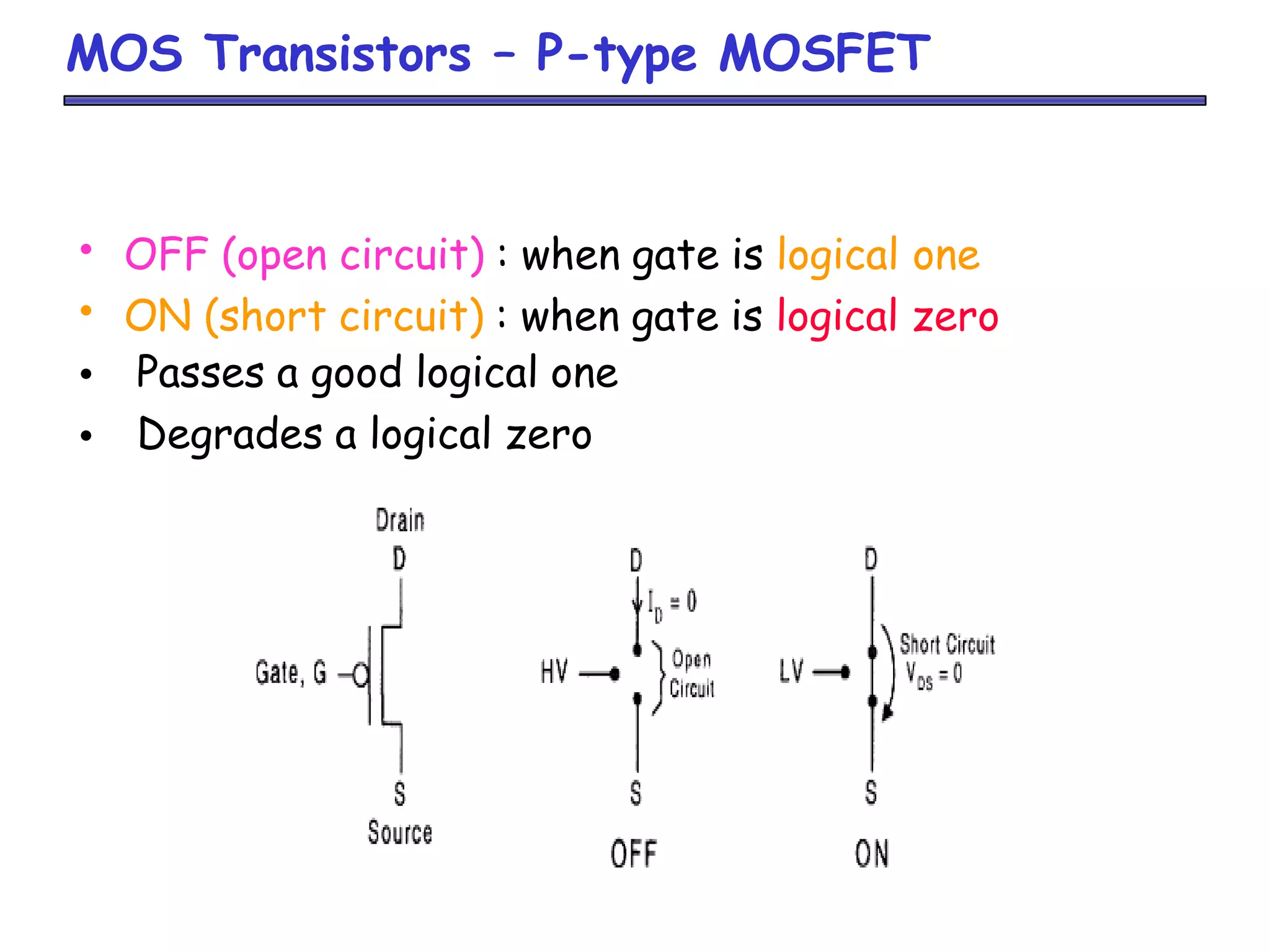
MOS Transistors –P-type MOSFET
• OFF (open circuit) : when gate is logical one
• ON (short circuit) : when gate is logical zero
•
•
Passes a good logical one
Degrades a logical zero
10.
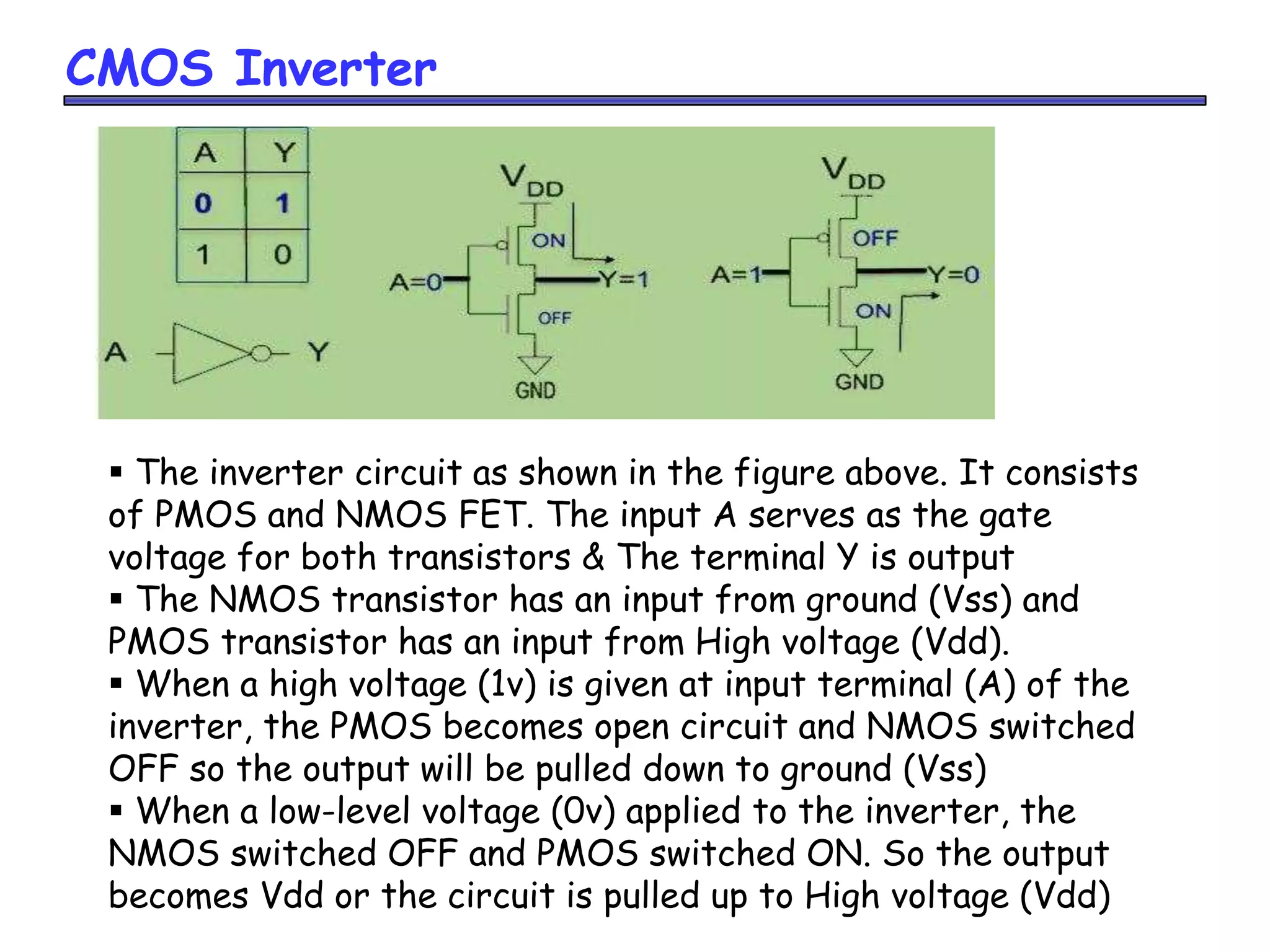
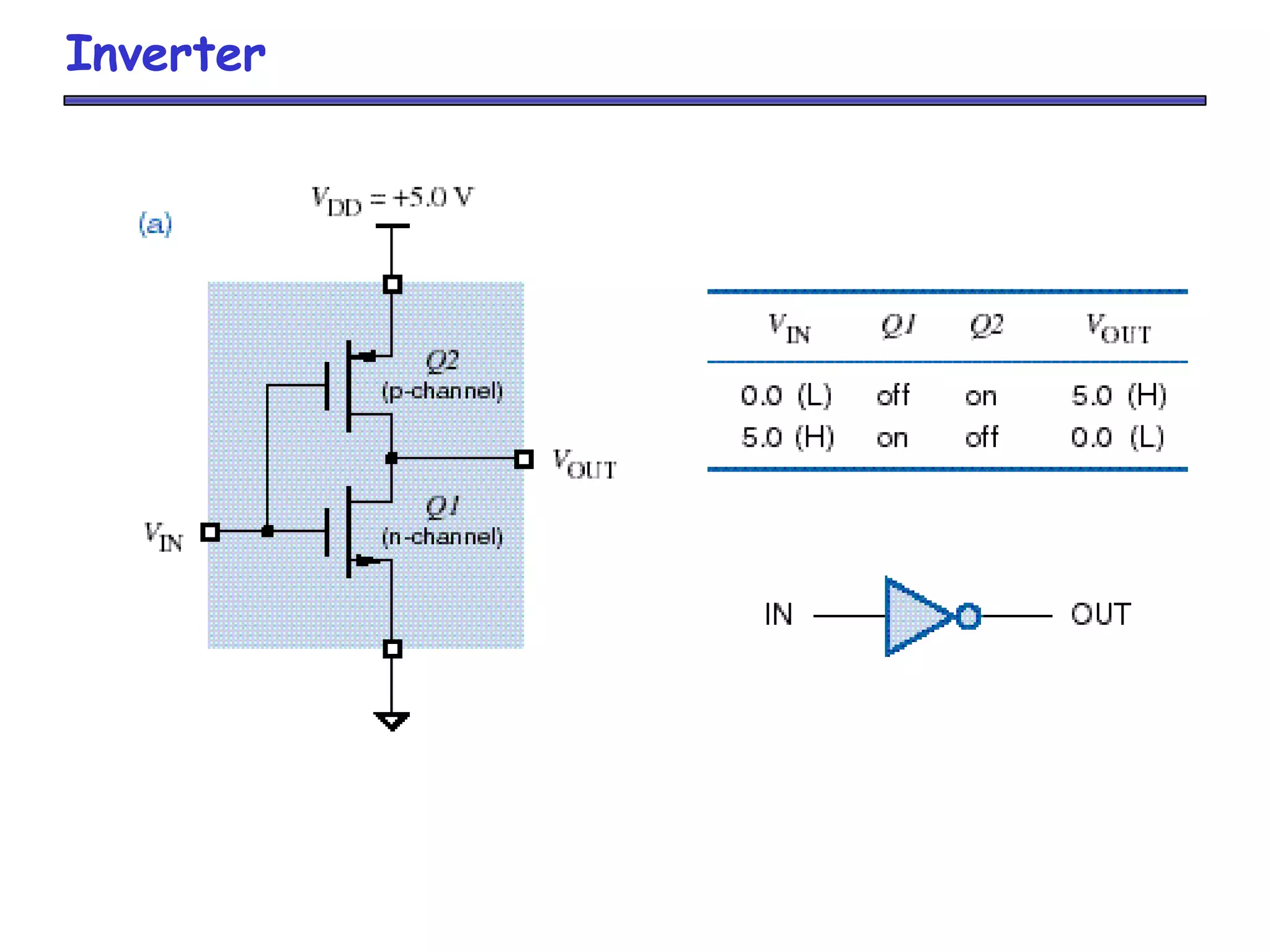
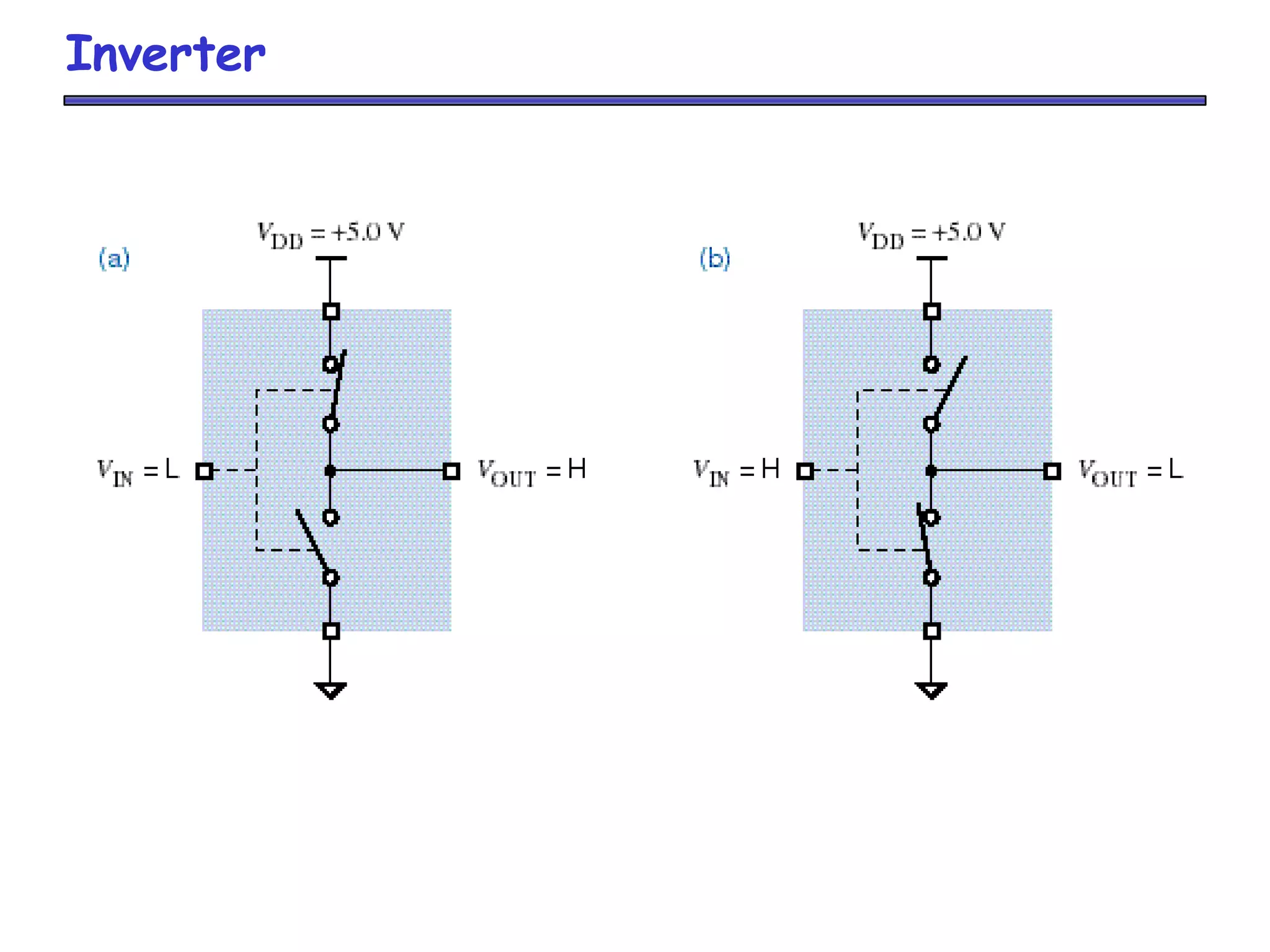
CMOS Inverter
Theinverter circuit as shown in the figure above. It consists
of PMOS and NMOS FET. The input A serves as the gate
voltage for both transistors & The terminal Y is output
The NMOS transistor has an input from ground (Vss) and
PMOS transistor has an input from High voltage (Vdd).
When a high voltage (1v) is given at input terminal (A) of the
inverter, the PMOS becomes open circuit and NMOS switched
OFF so the output will be pulled down to ground (Vss)
When a low-level voltage (0v) applied to the inverter, the
NMOS switched OFF and PMOS switched ON. So the output
becomes Vdd or the circuit is pulled up to High voltage (Vdd)
11.
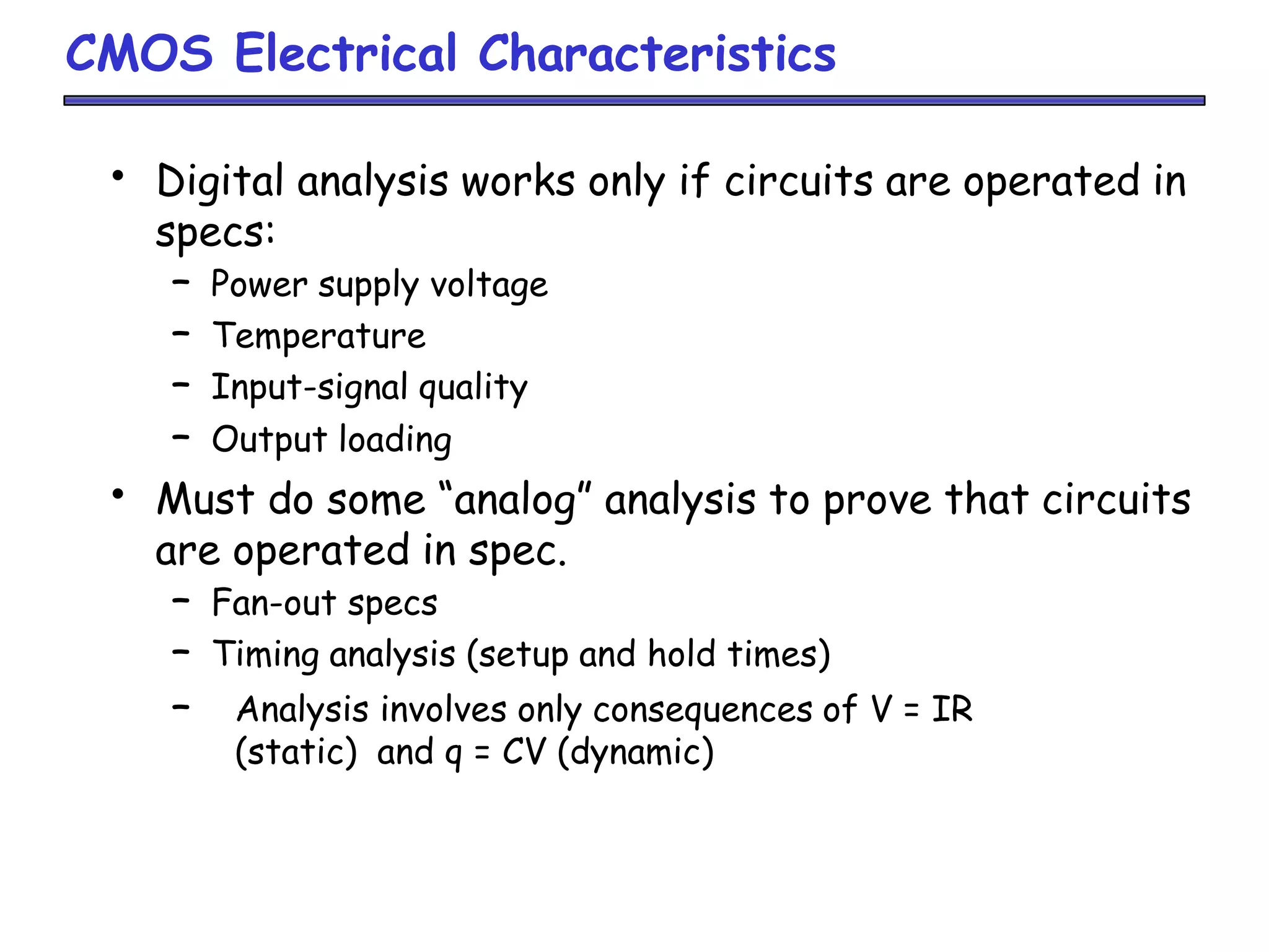
CMOS Electrical Characteristics
•Digital analysis works only if circuits are operated in
specs:
– Power supply voltage
– Temperature
– Input-signal quality
– Output loading
• Must do some “analog” analysis to prove that circuits
are operated in spec.
– Fan-out specs
– Timing analysis (setup and hold times)
– Analysis involves only consequences of V = IR
(static) and q = CV (dynamic)
12.
CMOS Electrical Characteristics
•Logic voltage levels
• DC noise margin
• DC Output Loading
• Fan-in
• Fan-out
• AC Loading (Speed)
• Transition Time
• Propagation Delay
• Power
13.
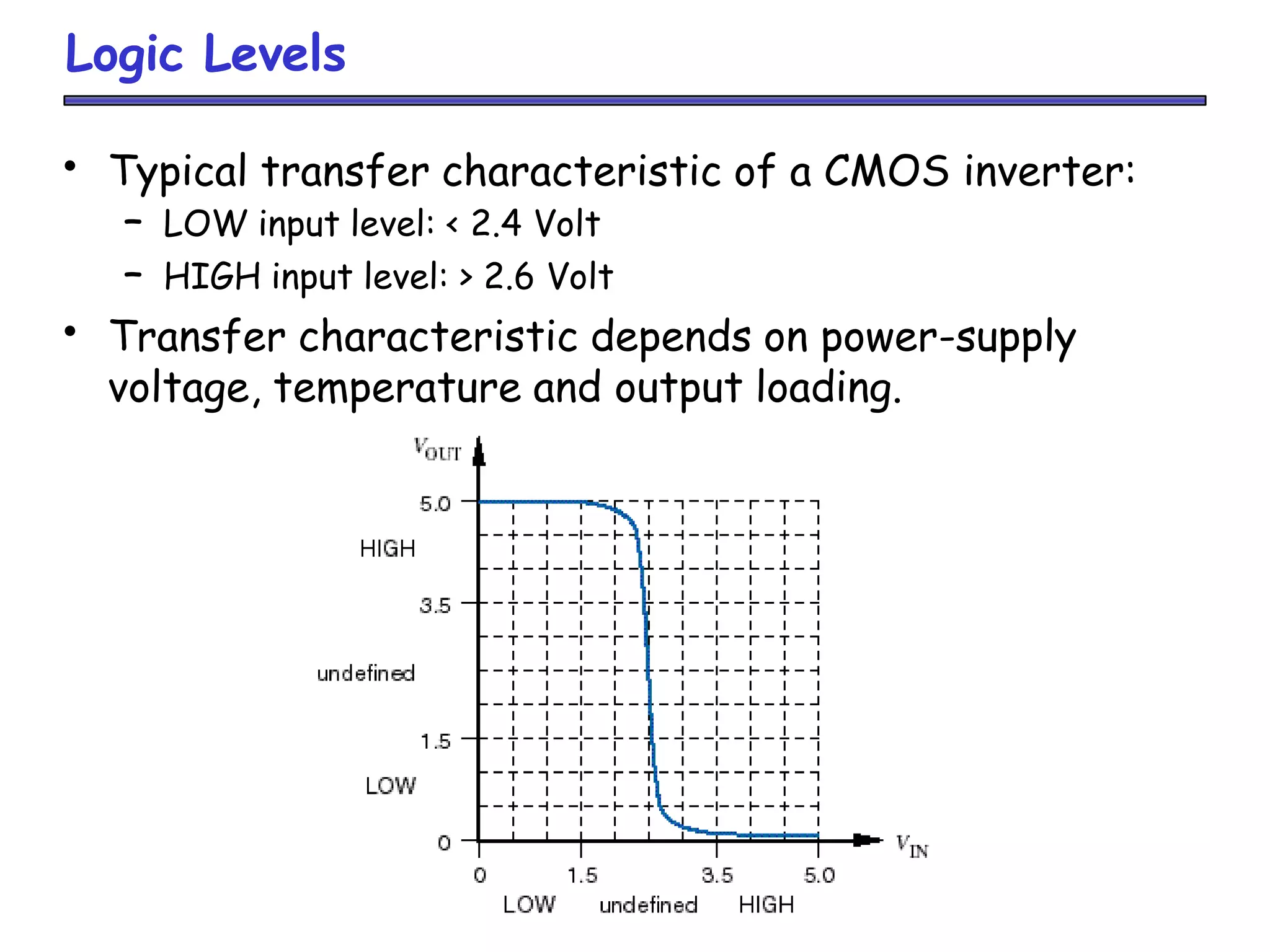
Logic Levels
• Typicaltransfer characteristic of a CMOS inverter:
– LOW input level: < 2.4 Volt
– HIGH input level: > 2.6 Volt
• Transfer characteristic depends on power-supply
voltage, temperature and output loading.
14.
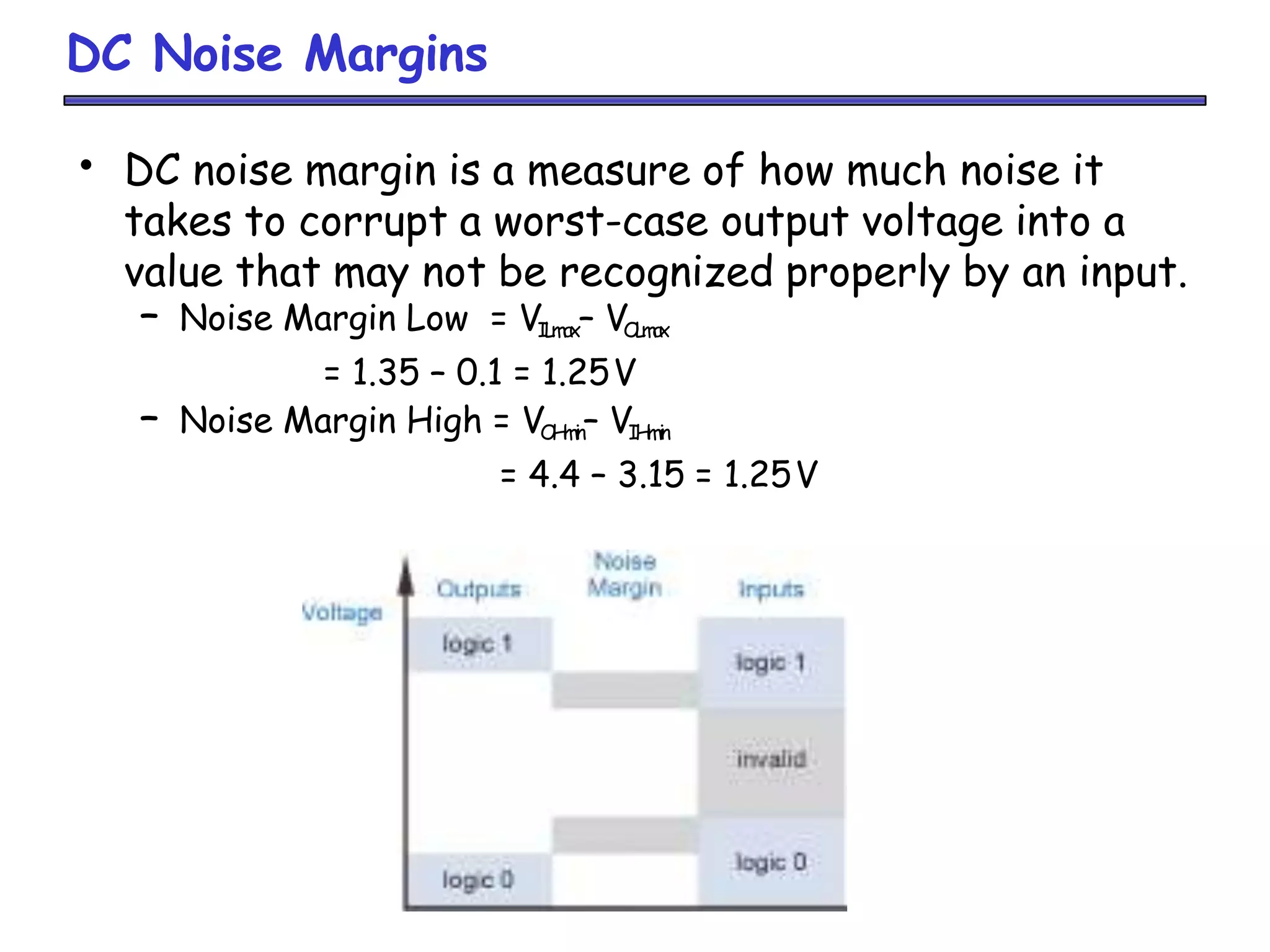
DC Noise Margins
•DC noise margin is a measure of how much noise it
takes to corrupt a worst-case output voltage into a
value that may not be recognized properly by an input.
– Noise Margin Low = VILmax– VOLmax
= 1.35 – 0.1 = 1.25V
– Noise Margin High = VOHmin– VIHmin
= 4.4 – 3.15 = 1.25V
15.
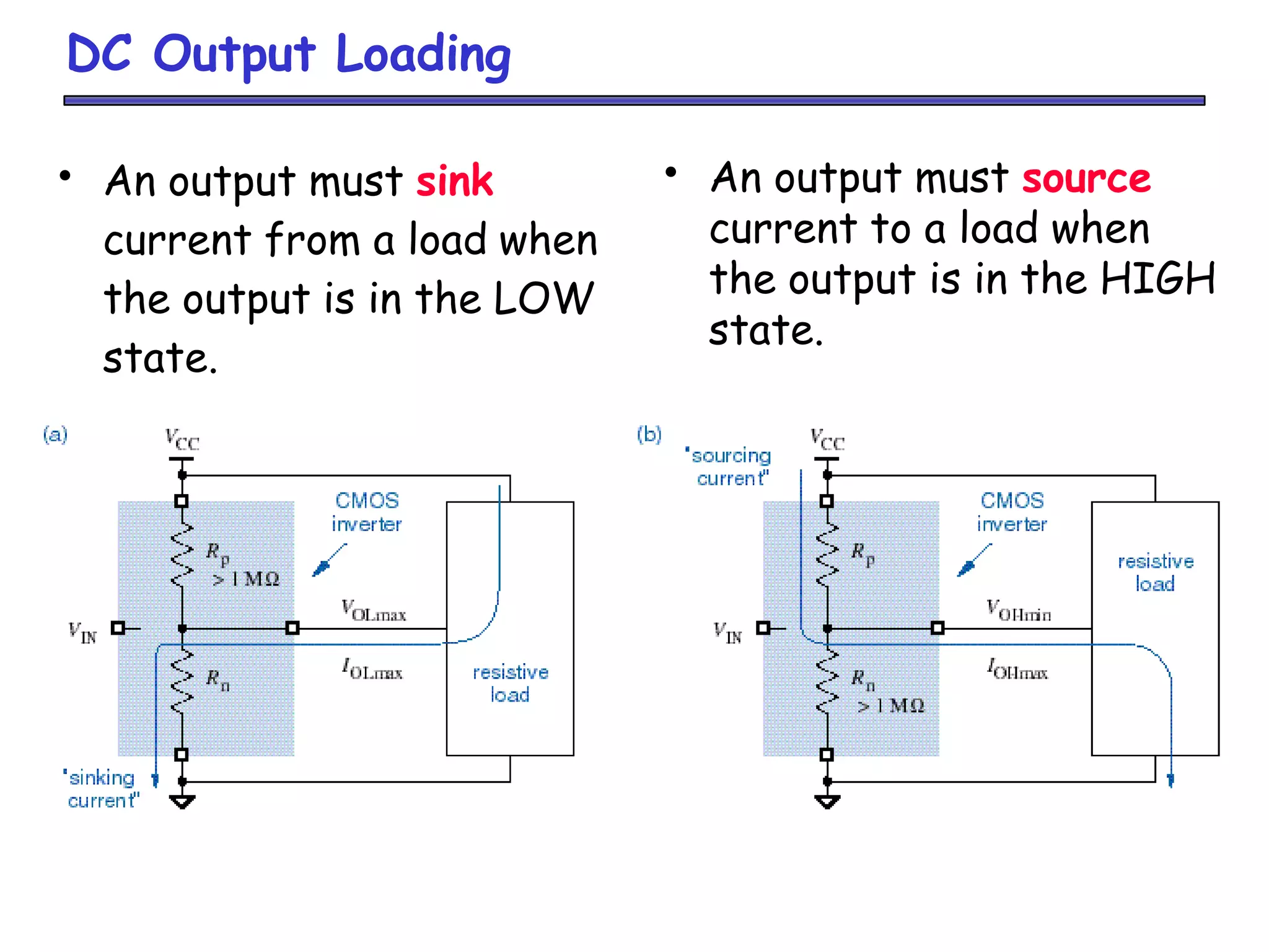
DC Output Loading
•An output must sink
current from a load when
the output is in the LOW
state.
• An output must source
current to a load when
the output is in the HIGH
state.
16.
DC Output Loading- Output-voltage Drops
• Resistance of “off” transistor is > 1 Megaohm, but
resistance of “on” transistor is nonzero,
– Voltage drops across “on” transistor, V = IR
• For “CMOS” loads, current and voltage drop are
negligible.
• For TTL inputs, LEDs, terminations, or other resistive
loads, current and voltage drop are significant and must
be calculated.
• If too much load, output voltage will go outside of valid
logic-voltage range.
– VOHmin,VIHmin
– VOLmax,VILmax
17.
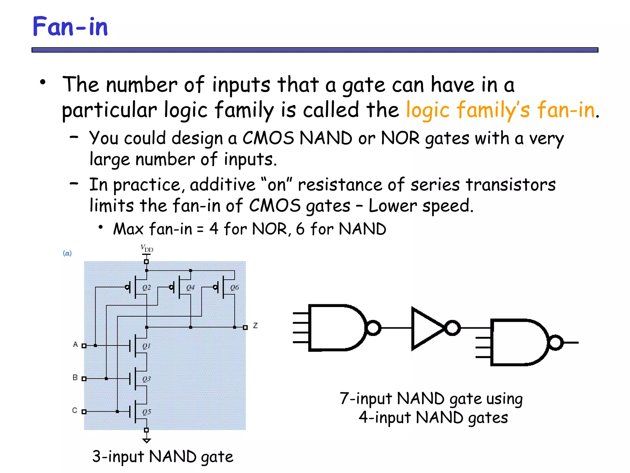
Fan-in
• The numberof inputs that a gate can have in a
particular logic family is called the logic family’s fan-in.
– You could design a CMOS NAND or NOR gates with a very
large number of inputs.
– In practice, additive “on” resistance of series transistors
limits the fan-in of CMOS gates – Lower speed.
• Max fan-in = 4 for NOR, 6 for NAND
3-input NAND gate
7-input NAND gate using
4-input NAND gates
18.
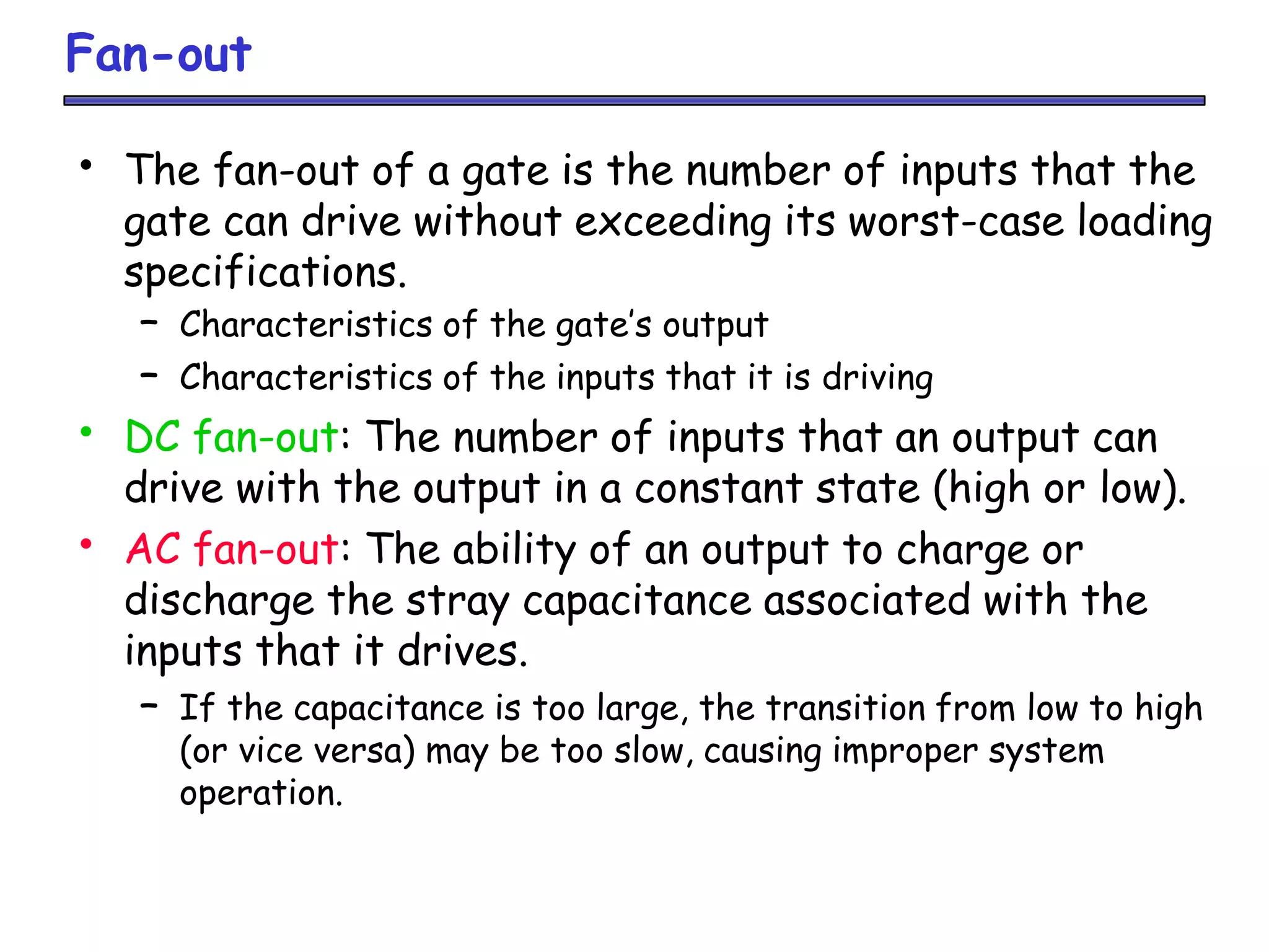
Fan-out
• The fan-outof a gate is the number of inputs that the
gate can drive without exceeding its worst-case loading
specifications.
– Characteristics of the gate’s output
– Characteristics of the inputs that it is driving
• DC fan-out: The number of inputs that an output can
drive with the output in a constant state (high or low).
• AC fan-out: The ability of an output to charge or
discharge the stray capacitance associated with the
inputs that it drives.
– If the capacitance is too large, the transition from low to high
(or vice versa) may be too slow, causing improper system
operation.
19.
AC Loading (Speed)
•AC loading has become a critical design factor as
industry has moved to pure CMOS systems.
– CMOS inputs have very high impedance, DC loading is
frequently negligible (low fan-outs).
– CMOS inputs and related packaging and wiring have significant
capacitance.
– Time to charge and discharge capacitance is a major
component of delay.
• Gate’s speed and power consumption depend on the AC
characteristics of the gate and its load.
20.
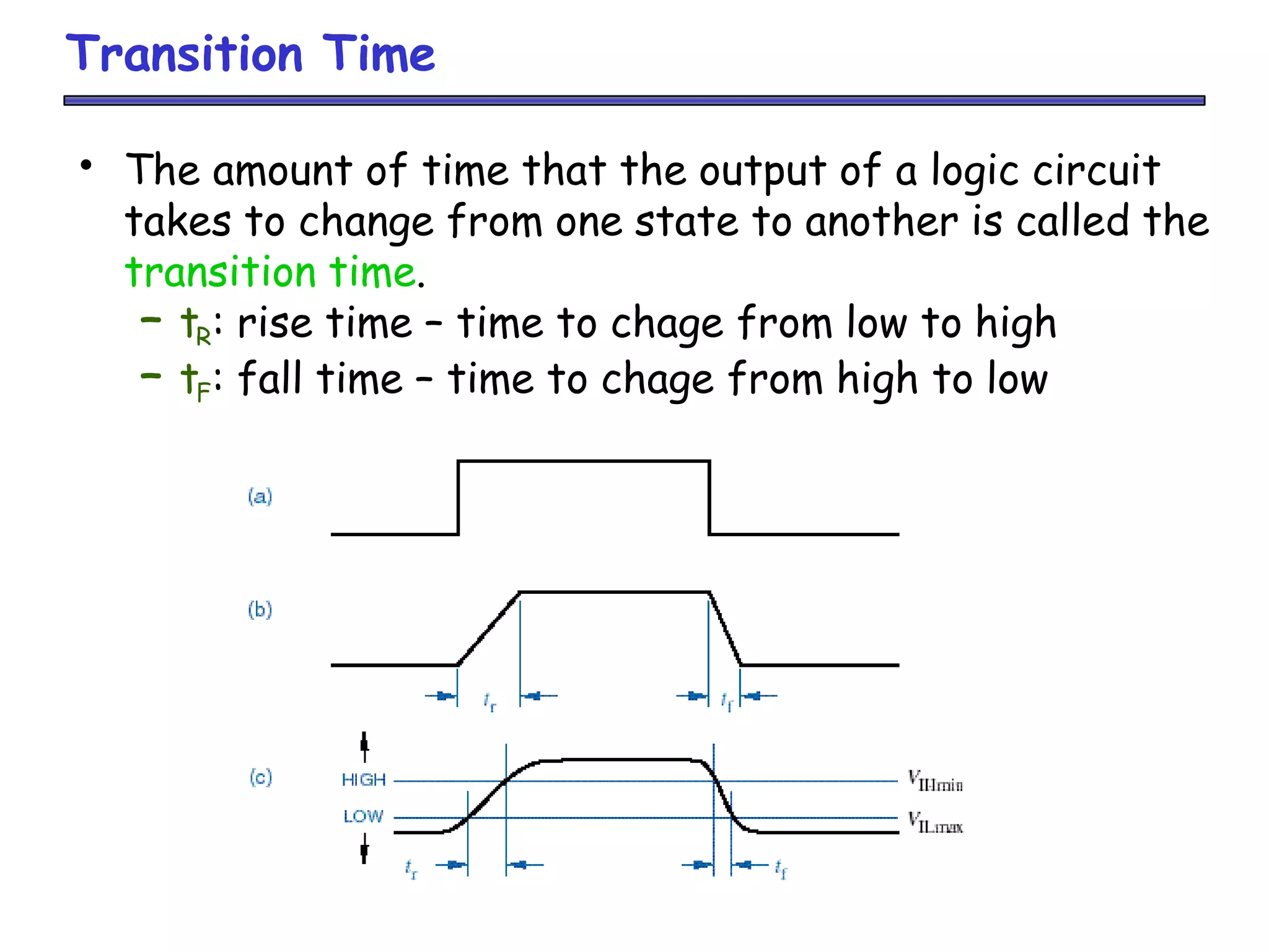
Transition Time
• Theamount of time that the output of a logic circuit
takes to change from one state to another is called the
transition time.
– tR: rise time – time to chage from low to high
– tF: fall time – time to chage from high to low
21.
Transition Time
• Therise and fall times of a CMOS output depend
mainly on
– “on” transistor resistance
– capacitive load
• Capacitive load = Stray capacitance = AC load
– Output circuits: A gate’s output transistors, internal wiring,
packaging
– The wiring that connects an output to other inputs
– Input circuits: A gate’s input transistors, internal wiring,
packaging
22.
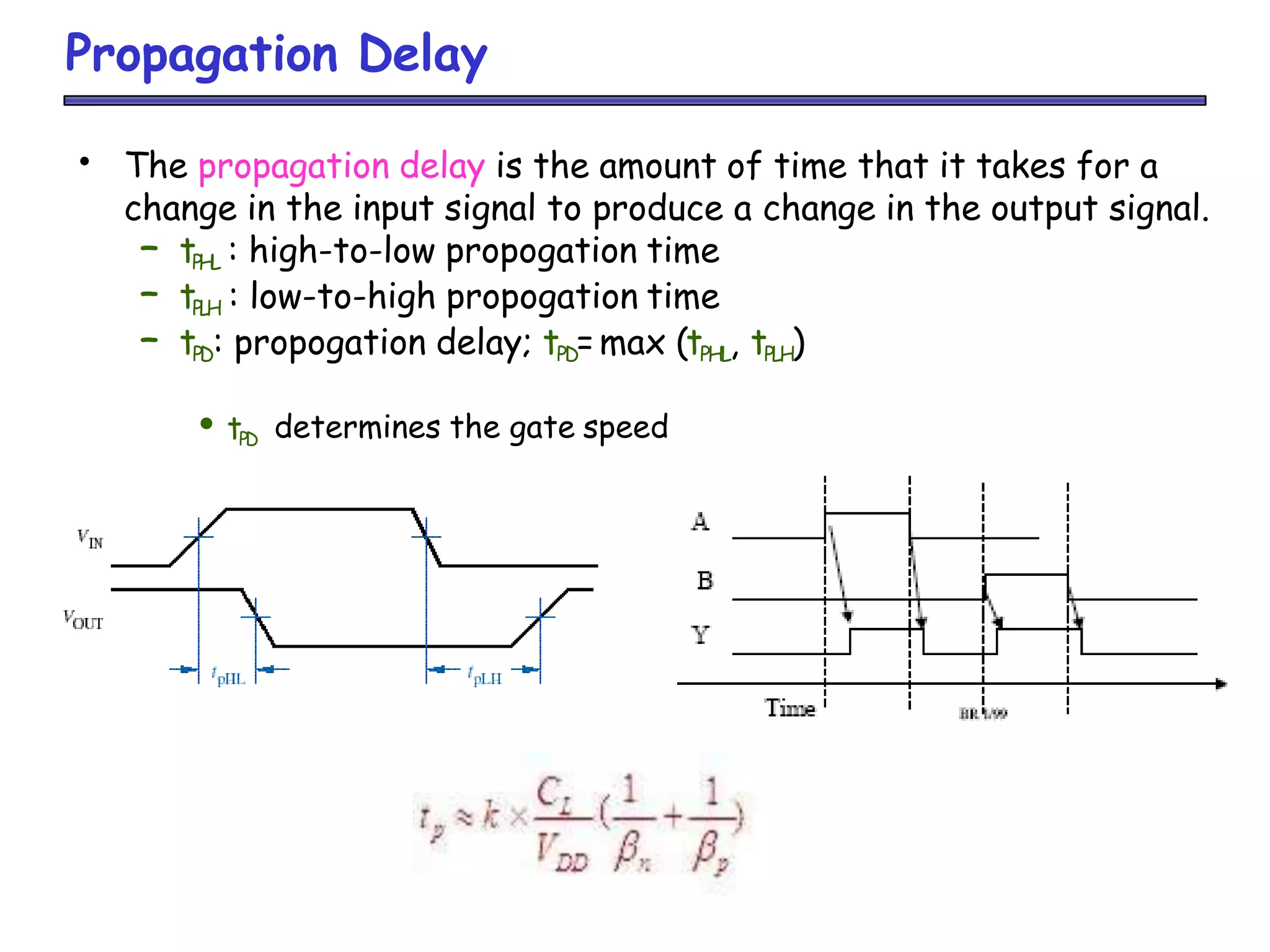
Propagation Delay
• Thepropagation delay is the amount of time that it takes for a
change in the input signal to produce a change in the output signal.
– tPHL : high-to-low propogation time
– tPLH : low-to-high propogation time
– tPD: propogation delay; tPD=max (tPHL, tPLH)
•tPD determines the gate speed
23.
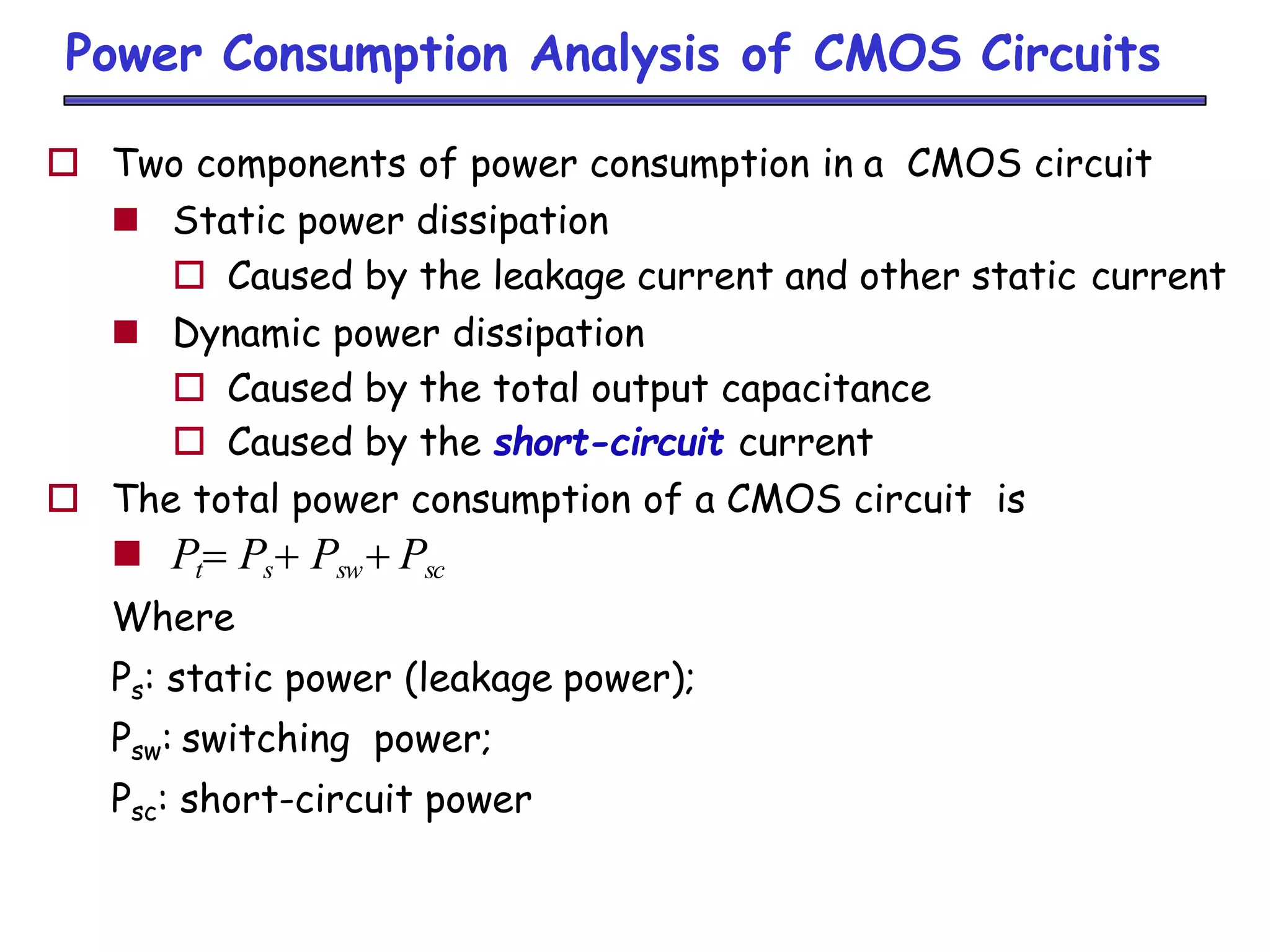
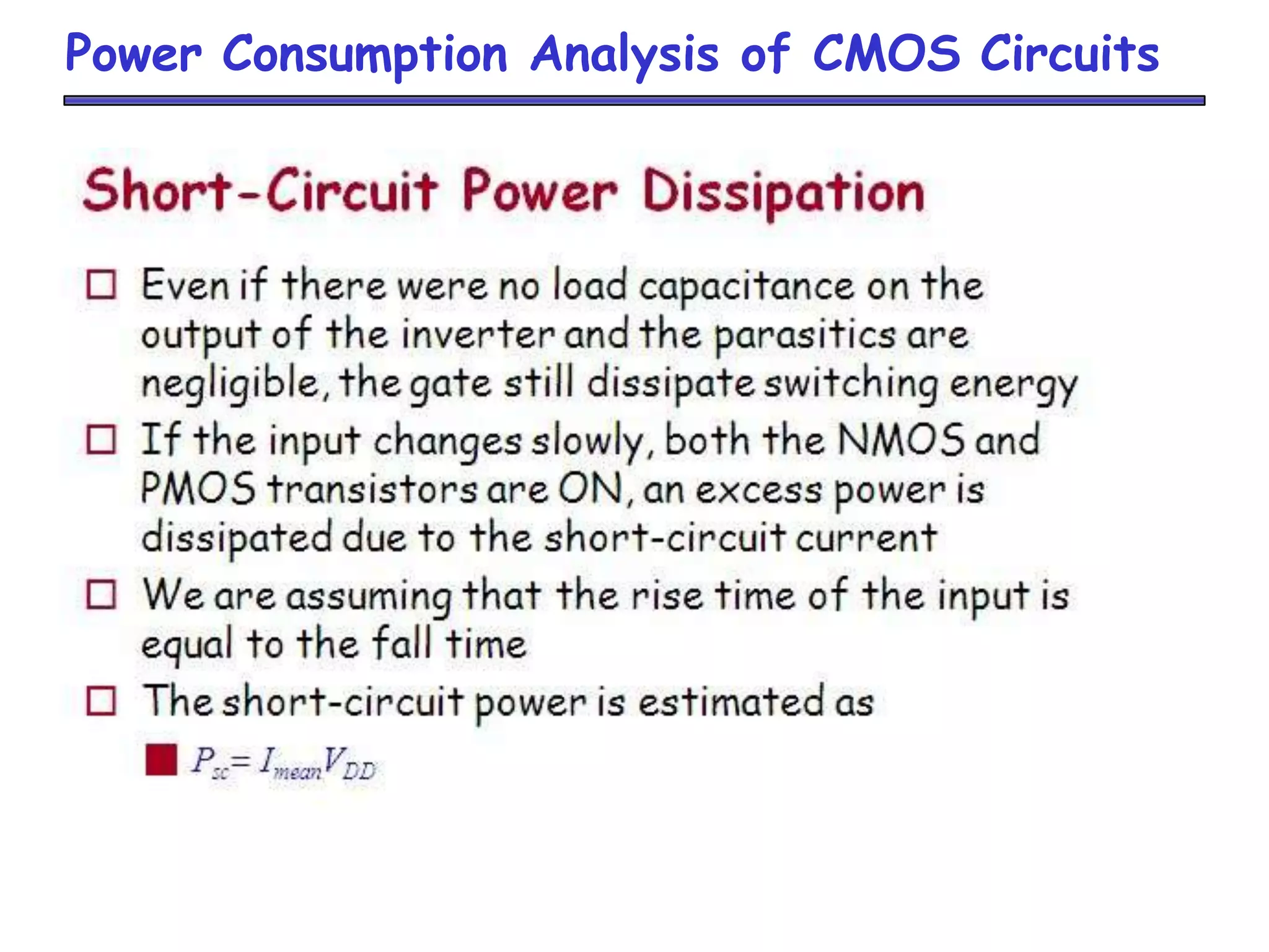
Power Consumption Analysisof CMOS Circuits
Two components of power consumption in a CMOS circuit
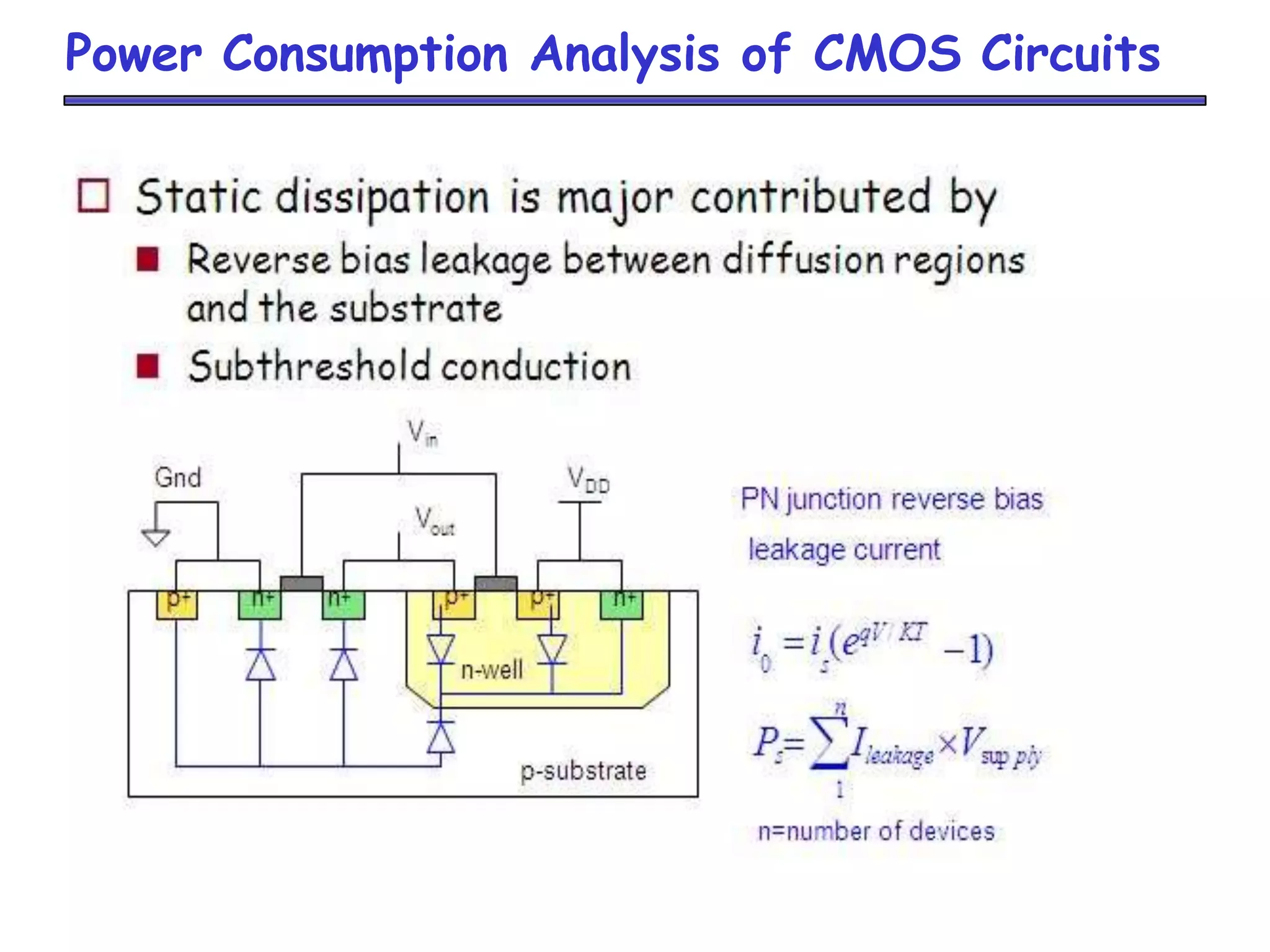
Static power dissipation
Caused by the leakage current and other static current
Dynamic power dissipation
Caused by the total output capacitance
Caused by the short-circuit current
The total power consumption of a CMOS circuit is
Pt Ps Psw Psc
Where
Ps: static power (leakage power);
Psw: switching power;
Psc: short-circuit power
Power Consumption Analysisof CMOS Circuits
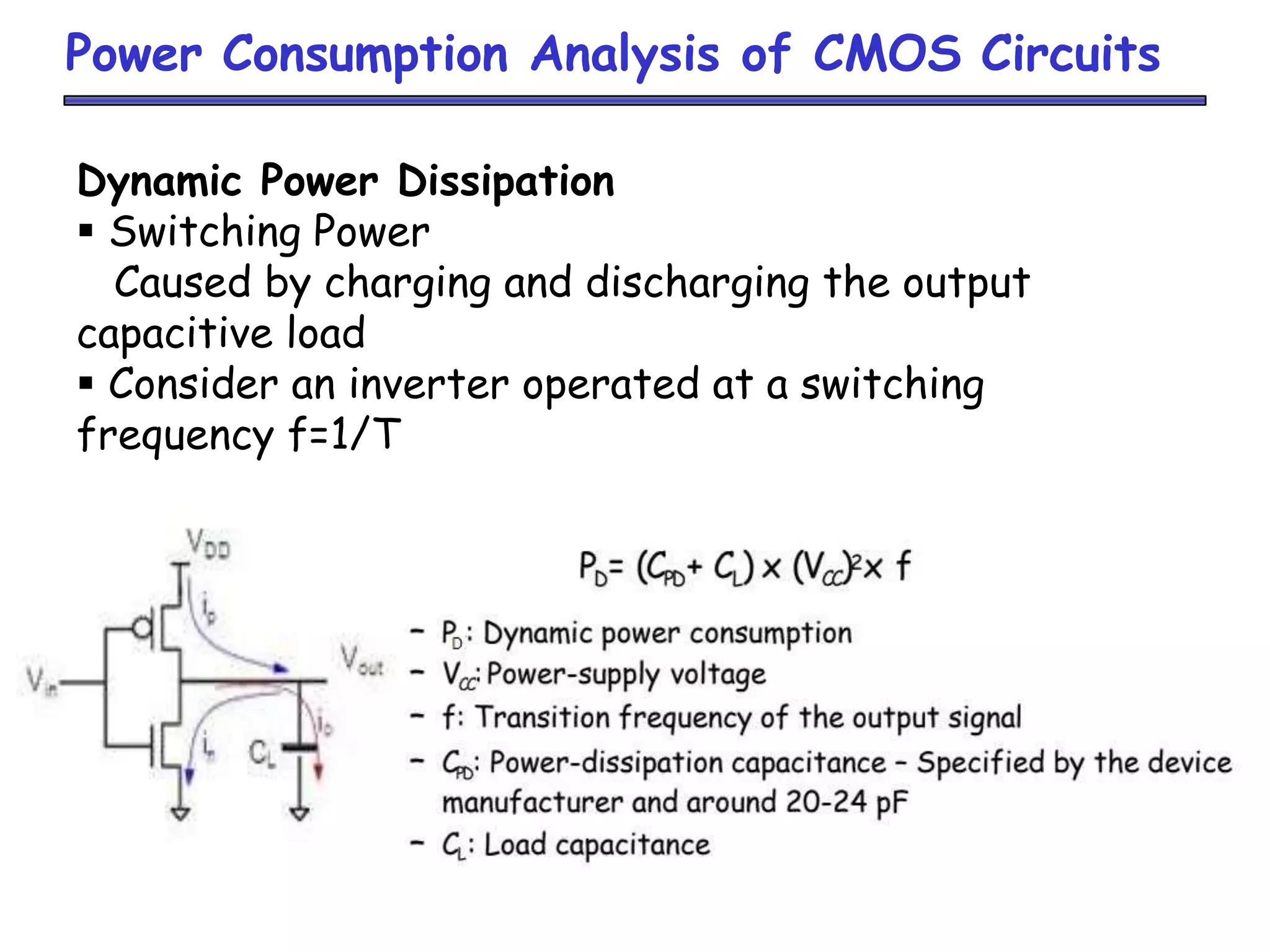
Dynamic Power Dissipation
Switching Power
Caused by charging and discharging the output
capacitive load
Consider an inverter operated at a switching
frequency f=1/T
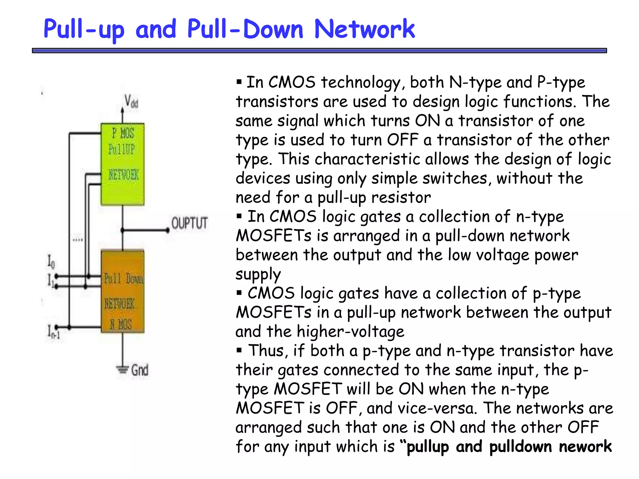
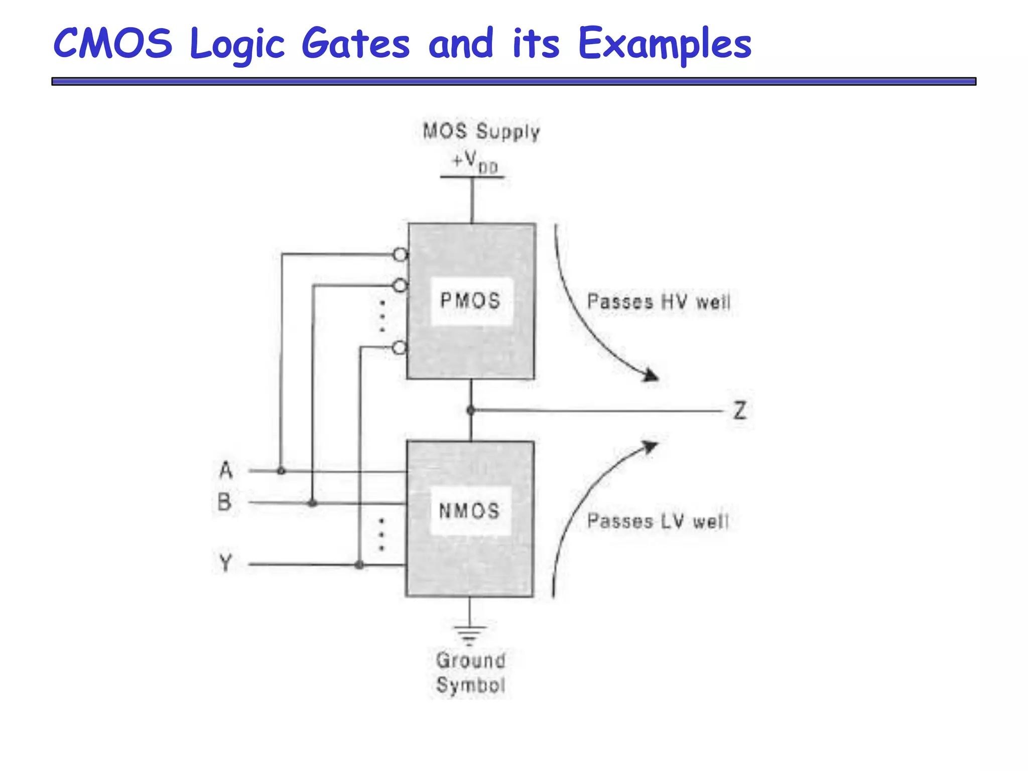
Pull-up and Pull-DownNetwork
In CMOS technology, both N-type and P-type
transistors are used to design logic functions. The
same signal which turns ON a transistor of one
type is used to turn OFF a transistor of the other
type. This characteristic allows the design of logic
devices using only simple switches, without the
need for a pull-up resistor
In CMOS logic gates a collection of n-type
MOSFETs is arranged in a pull-down network
between the output and the low voltage power
supply
CMOS logic gates have a collection of p-type
MOSFETs in a pull-up network between the output
and the higher-voltage
Thus, if both a p-type and n-type transistor have
their gates connected to the same input, the p-
type MOSFET will be ON when the n-type
MOSFET is OFF, and vice-versa. The networks are
arranged such that one is ON and the other OFF
for any input which is “pullup and pulldown nework
28.
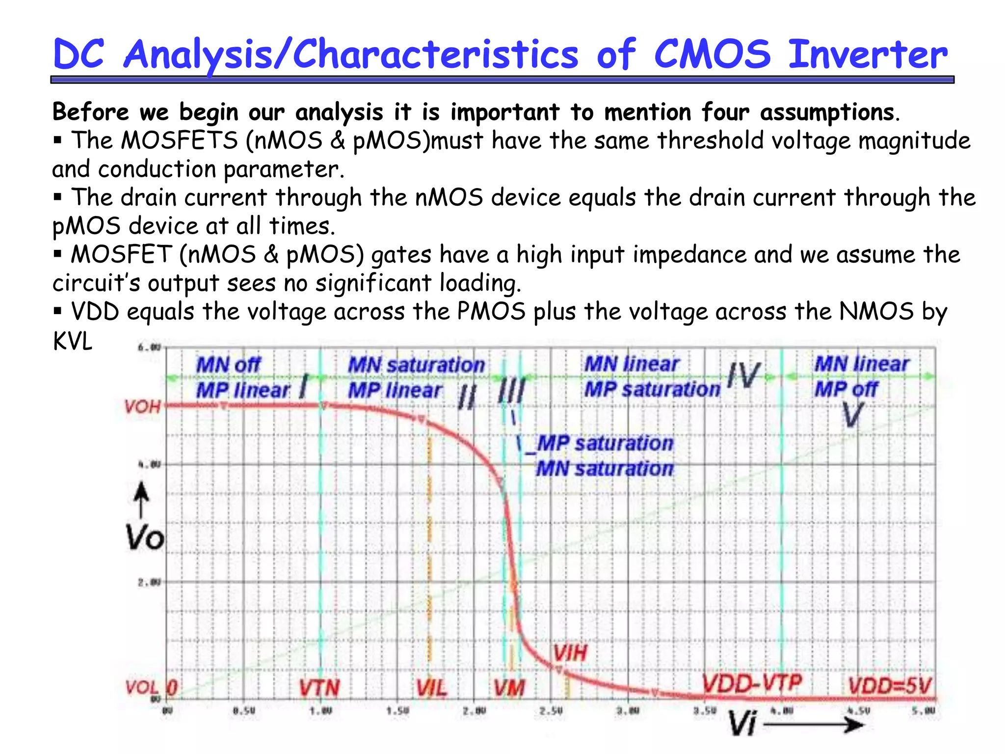
DC Analysis/Characteristics ofCMOS Inverter
Before we begin our analysis it is important to mention four assumptions.
The MOSFETS (nMOS & pMOS)must have the same threshold voltage magnitude
and conduction parameter.
The drain current through the nMOS device equals the drain current through the
pMOS device at all times.
MOSFET (nMOS & pMOS) gates have a high input impedance and we assume the
circuit’s output sees no significant loading.
VDD equals the voltage across the PMOS plus the voltage across the NMOS by
KVL.
29.
DC Analysis/Characteristics ofCMOS Inverter
Region I
In this case when we apply an input voltage between 0 and VTN.
The PMOS device on since a low voltage is being applied to it.
The NMOS device is off, there is no current flow through either device.
VDD is available at the Vo terminal
•The PMOS device is forward biased (VSG > -VTP) and therefore on.
•This MOSFET is in the linear region (VSD <= VSG + VTP=VDD - Vo + VTP).
•The NMOS device is cut off since the input voltage is below VTN
(Vi=VGS<VTN).
•The power dissipation is zero.
Region II
Here we raise the input voltage above VTN. We find that the PMOS device
remains in the linear. The NMOS turns on
•The PMOS device is in the linear region (VSD <= VSG + VTP).
•The NMOS device is in the saturation region (Vi = Vo - VTN).
•Current now flows through both devices. Power dissipation is no longer zero.
The maximum allowable input voltage at the low logic state (VIL)
occurs in this region
30.
DC Analysis/Characteristics ofCMOS Inverter
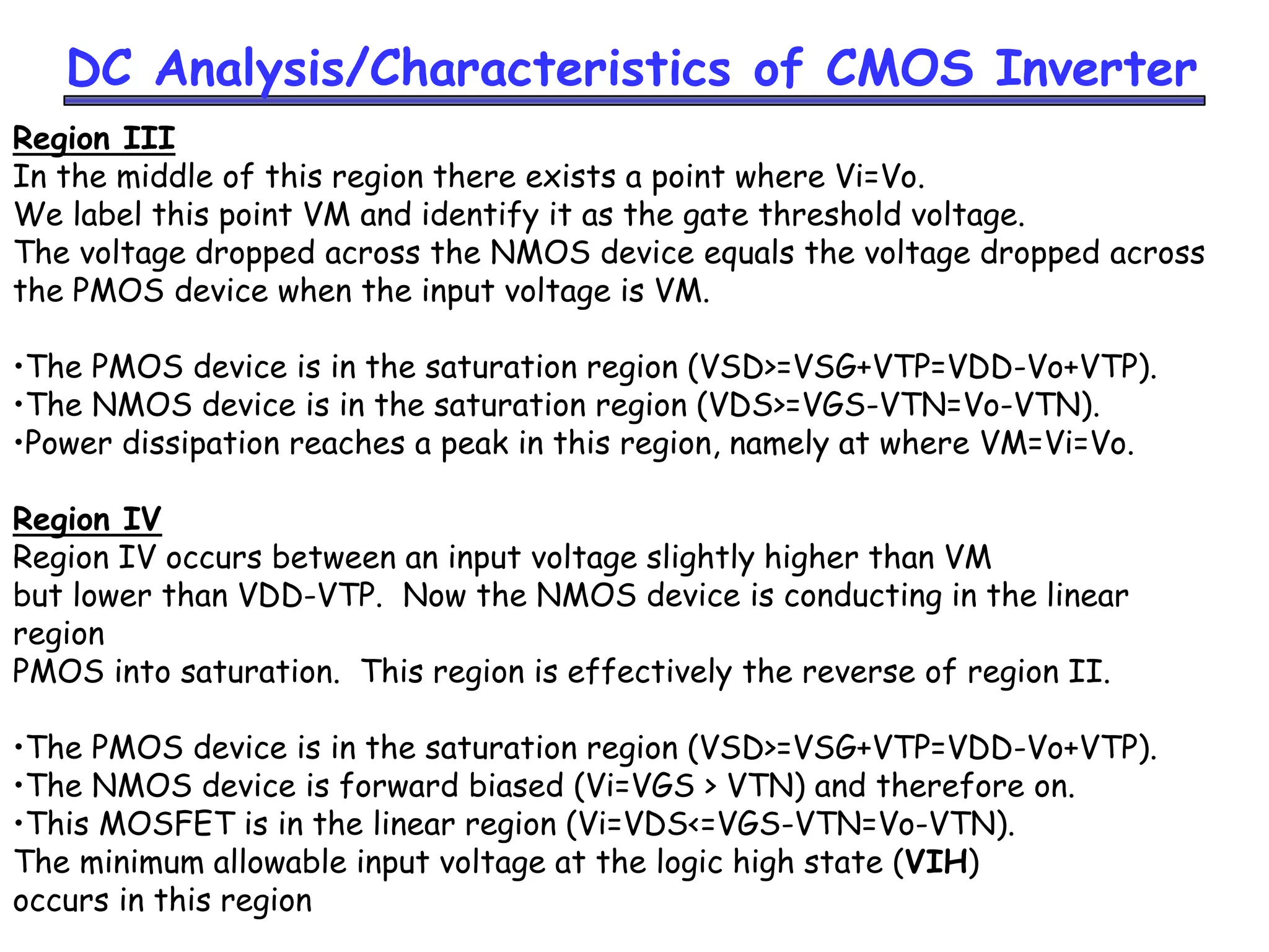
Region III
In the middle of this region there exists a point where Vi=Vo.
We label this point VM and identify it as the gate threshold voltage.
The voltage dropped across the NMOS device equals the voltage dropped across
the PMOS device when the input voltage is VM.
•The PMOS device is in the saturation region (VSD>=VSG+VTP=VDD-Vo+VTP).
•The NMOS device is in the saturation region (VDS>=VGS-VTN=Vo-VTN).
•Power dissipation reaches a peak in this region, namely at where VM=Vi=Vo.
Region IV
Region IV occurs between an input voltage slightly higher than VM
but lower than VDD-VTP. Now the NMOS device is conducting in the linear
region
PMOS into saturation. This region is effectively the reverse of region II.
•The PMOS device is in the saturation region (VSD>=VSG+VTP=VDD-Vo+VTP).
•The NMOS device is forward biased (Vi=VGS > VTN) and therefore on.
•This MOSFET is in the linear region (Vi=VDS<=VGS-VTN=Vo-VTN).
The minimum allowable input voltage at the logic high state (VIH)
occurs in this region
31.
DC Analysis/Characteristics ofCMOS Inverter
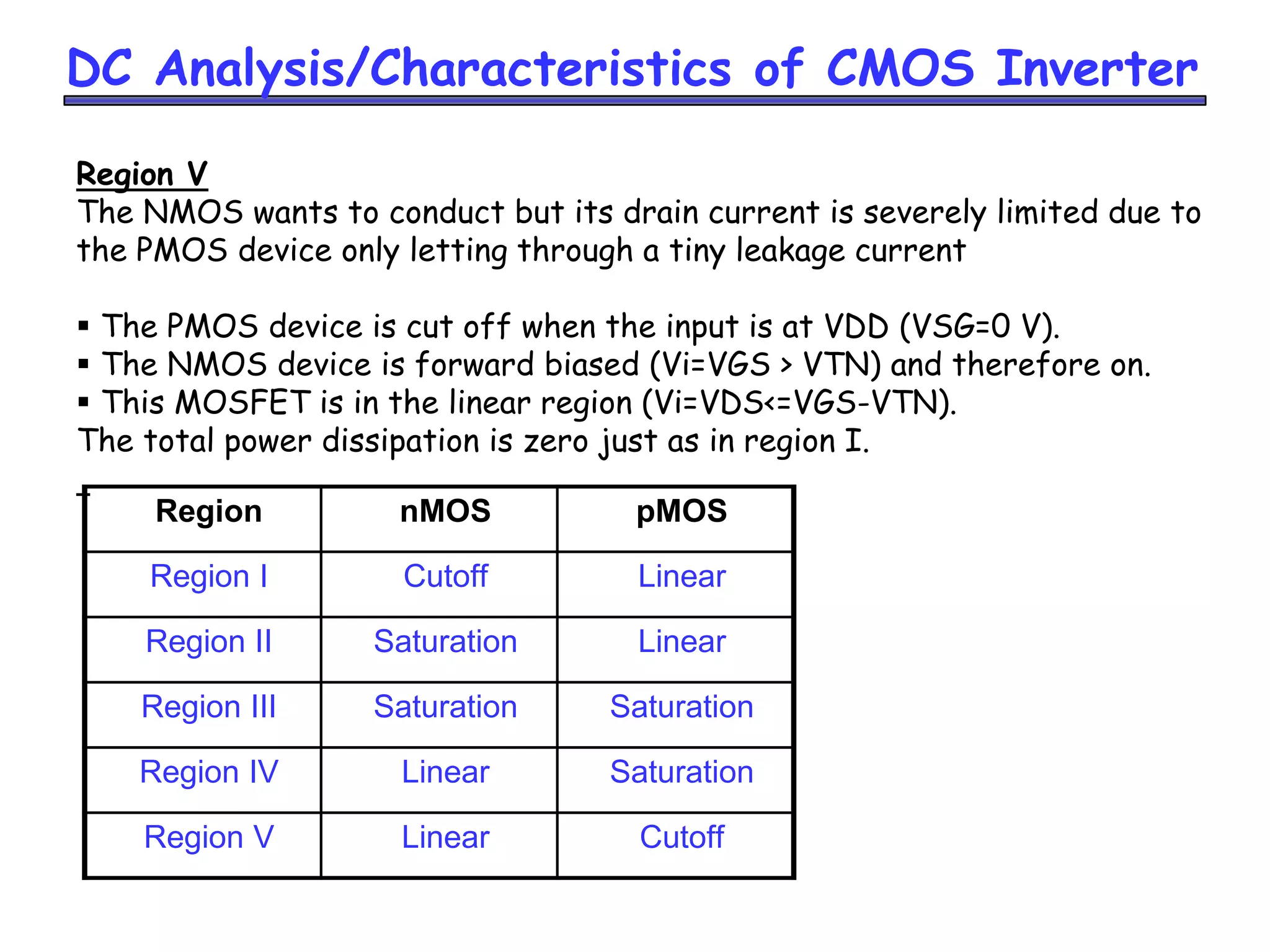
Region V
The NMOS wants to conduct but its drain current is severely limited due to
the PMOS device only letting through a tiny leakage current
The PMOS device is cut off when the input is at VDD (VSG=0 V).
The NMOS device is forward biased (Vi=VGS > VTN) and therefore on.
This MOSFET is in the linear region (Vi=VDS<=VGS-VTN).
The total power dissipation is zero just as in region I.
Region nMOS pMOS
Region I Cutoff Linear
Region II Saturation Linear
Region III Saturation Saturation
Region IV Linear Saturation
Region V Linear Cutoff
32.
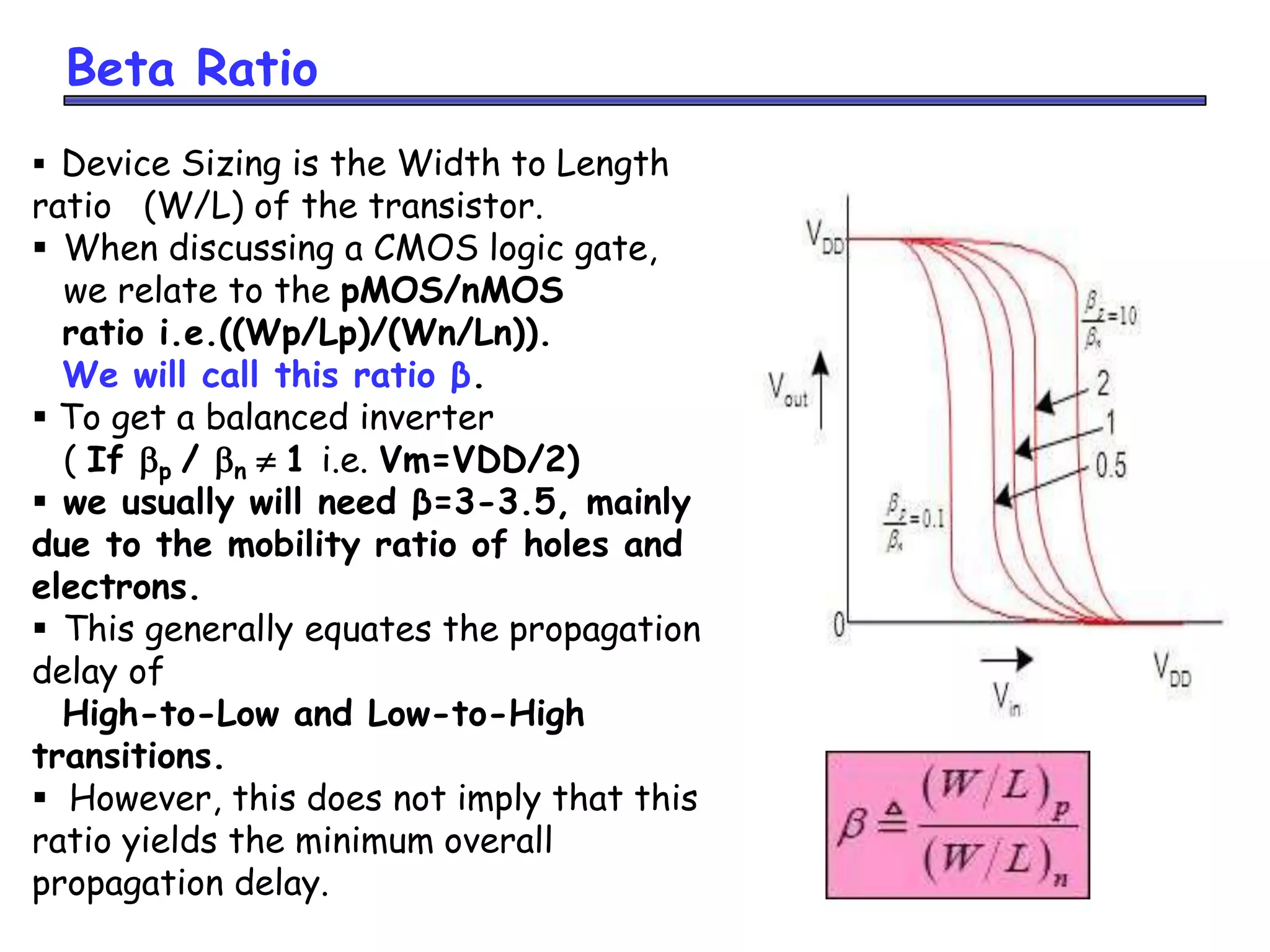
Beta Ratio
DeviceSizing is the Width to Length
ratio (W/L) of the transistor.
When discussing a CMOS logic gate,
we relate to the pMOS/nMOS
ratio i.e.((Wp/Lp)/(Wn/Ln)).
We will call this ratio β.
To get a balanced inverter
( If p / n 1 i.e. Vm=VDD/2)
we usually will need β=3-3.5, mainly
due to the mobility ratio of holes and
electrons.
This generally equates the propagation
delay of
High-to-Low and Low-to-High
transitions.
However, this does not imply that this
ratio yields the minimum overall
propagation delay.
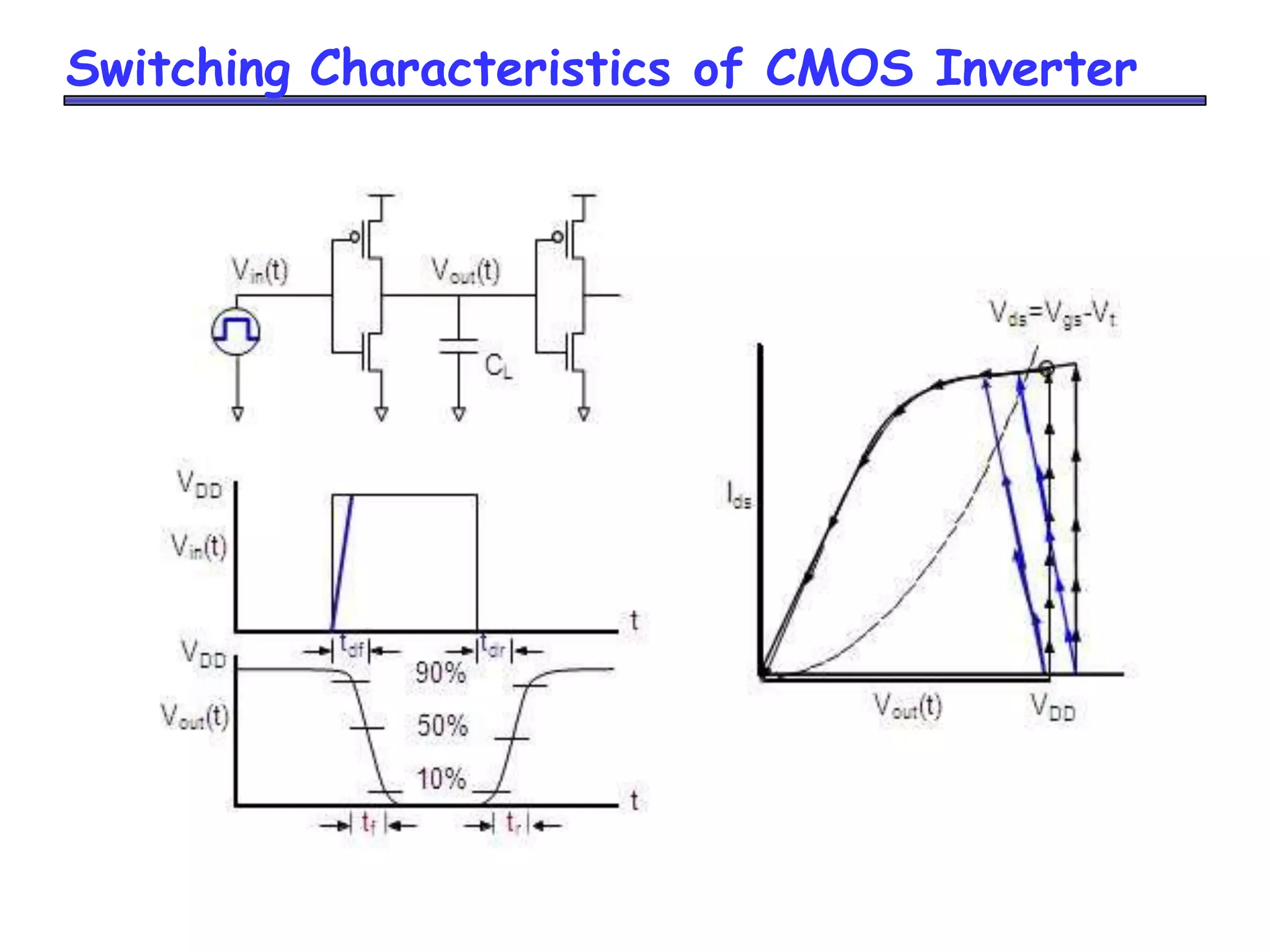
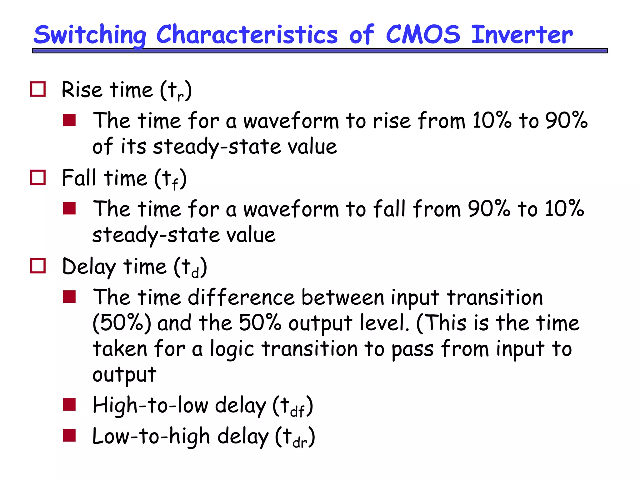
Switching Characteristics ofCMOS Inverter
Rise time (tr)
The time for a waveform to rise from 10% to 90%
of its steady-state value
Fall time (tf)
The time for a waveform to fall from 90% to 10%
steady-state value
Delay time (td)
The time difference between input transition
(50%) and the 50% output level. (This is the time
taken for a logic transition to pass from input to
output
High-to-low delay (tdf)
Low-to-high delay (tdr)