Tamil Call Girls Bhayandar WhatsApp +91-9930687706, Best Service
cmos 2.pdf
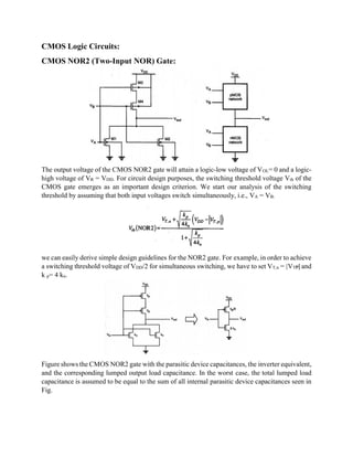
1. CMOS Logic Circuits:
CMOS NOR2 (Two-Input NOR) Gate:
The output voltage of the CMOS NOR2 gate will attain a logic-low voltage of VOL= 0 and a logic-
high voltage of VR = VDD. For circuit design purposes, the switching threshold voltage Vth of the
CMOS gate emerges as an important design criterion. We start our analysis of the switching
threshold by assuming that both input voltages switch simultaneously, i.e., VA = VB.
we can easily derive simple design guidelines for the NOR2 gate. For example, in order to achieve
a switching threshold voltage of VDD/2 for simultaneous switching, we have to set VT,n = |VTP| and
k p= 4 kn.
Figure shows the CMOS NOR2 gate with the parasitic device capacitances, the inverter equivalent,
and the corresponding lumped output load capacitance. In the worst case, the total lumped load
capacitance is assumed to be equal to the sum of all internal parasitic device capacitances seen in
Fig.
2. Fig. Parasitic device capacitances of the CMOS equivalent with the lumped output load capacitance.
NOR2 circuit and the simplified
CMOS NAND2 (2-Input NAND) Gate:
Figure shows a two-input CMOS NAND (NAND2) gate. The operating principle of this circuit is
the exact dual of the CMOS NOR2 operation examined earlier. The n-net consisting of two series-
connected NMOS transistors creates a conducting path between the output node and the ground
only if both input voltages are logic-high, i.e., are equal to VOH. In this case, both of the parallel-
connected PMOS transistors in the p-net will be off. For all other input combinations, either one
or both of the PMOS transistors will be turned on, while the n-net is cut-off, thus creating a current
path between the output node and the power supply voltage.
Using an analysis similar to the one developed for the NOR2 gate, we can easily calculate the
switching threshold for the CMOS NAND2 gate. Again, we will assume that the device sizes in
each block are identical, with (W/L)n,A= (W/L)n,B and (W/L)P,A=(W/L)p,B.The switching threshold
for this gate is then found as
3. Fig. A CMOS NAND2 gate and its inverter equivalent
A switching threshold voltage of VDD/2 (for simultaneous switching) is achieved by setting VT,n =
|VT,p| and kn=4kp in the NAND2.