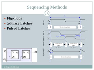
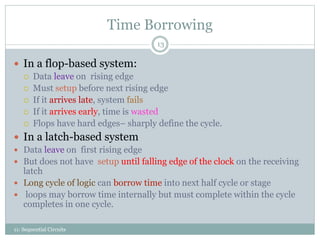
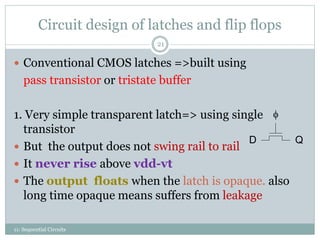
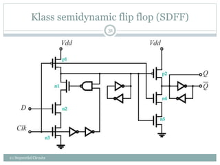
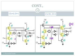
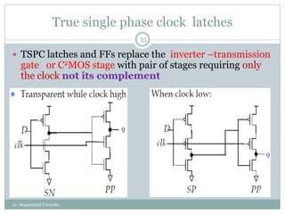
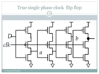
This document discusses sequential circuits and their design. It covers:
1. The difference between combinational and sequential logic and examples like finite state machines and pipelines that require sequential logic.
2. Methods for sequencing tokens through pipelines using flip-flops, latches, and pulsed latches and the associated timing diagrams.
3. Design considerations for sequential circuits like max/min delays, time borrowing, and clock skew.
4. Circuit designs for various latches and flip-flops including transparent latches, CMOS transmission gate latches, dynamic flip-flops, and true single phase clock elements.
FPGA are a special form of Programmable logic devices(PLDs) with higher densities as compared to custom ICs and capable of implementing functionality in a short period of time using computer aided design (CAD) software....by mathewsubin3388@gmail.com
The document explains about the concepts of sequential circuits in Digital electronics.
This will be helpful for the beginners in VLSI and electronics students.
This presentation discusses the basics about how to realize logic functions using Static CMOS logic. This presentation discusses about how to realize a Boolean expression by drawing a Pull-up network and a pull-down network. It also briefs about the pass transistor logic and the concepts of weak and strong outputs.
Routing in Integrated circuits is an important task which requires extreme care while placing the modules and circuits and connecting them with each other.
Unit II- TRANSMISSION CHARACTERISTIC OF OPTICAL FIBER tamil arasan
Attenuation - Absorption losses, Scattering losses, Bending Losses, Core and Cladding losses, Signal Distortion in Optical Wave guides-Information Capacity determination -Group Delay-Material Dispersion, Wave guide Dispersion, Signal distortion in SM fibers-Polarization Mode dispersion, Intermodal dispersion, -Design Optimization of SM fibers-RI profile and cut-off wavelength.
CFD Simulation of By-pass Flow in a HRSG module by R&R Consult.pptxR&R Consult
CFD analysis is incredibly effective at solving mysteries and improving the performance of complex systems!
Here's a great example: At a large natural gas-fired power plant, where they use waste heat to generate steam and energy, they were puzzled that their boiler wasn't producing as much steam as expected.
R&R and Tetra Engineering Group Inc. were asked to solve the issue with reduced steam production.
An inspection had shown that a significant amount of hot flue gas was bypassing the boiler tubes, where the heat was supposed to be transferred.
R&R Consult conducted a CFD analysis, which revealed that 6.3% of the flue gas was bypassing the boiler tubes without transferring heat. The analysis also showed that the flue gas was instead being directed along the sides of the boiler and between the modules that were supposed to capture the heat. This was the cause of the reduced performance.
Based on our results, Tetra Engineering installed covering plates to reduce the bypass flow. This improved the boiler's performance and increased electricity production.
It is always satisfying when we can help solve complex challenges like this. Do your systems also need a check-up or optimization? Give us a call!
Work done in cooperation with James Malloy and David Moelling from Tetra Engineering.
More examples of our work https://www.r-r-consult.dk/en/cases-en/
Saudi Arabia stands as a titan in the global energy landscape, renowned for its abundant oil and gas resources. It's the largest exporter of petroleum and holds some of the world's most significant reserves. Let's delve into the top 10 oil and gas projects shaping Saudi Arabia's energy future in 2024.
Water scarcity is the lack of fresh water resources to meet the standard water demand. There are two type of water scarcity. One is physical. The other is economic water scarcity.
Final project report on grocery store management system..pdfKamal Acharya
In today’s fast-changing business environment, it’s extremely important to be able to respond to client needs in the most effective and timely manner. If your customers wish to see your business online and have instant access to your products or services.
Online Grocery Store is an e-commerce website, which retails various grocery products. This project allows viewing various products available enables registered users to purchase desired products instantly using Paytm, UPI payment processor (Instant Pay) and also can place order by using Cash on Delivery (Pay Later) option. This project provides an easy access to Administrators and Managers to view orders placed using Pay Later and Instant Pay options.
In order to develop an e-commerce website, a number of Technologies must be studied and understood. These include multi-tiered architecture, server and client-side scripting techniques, implementation technologies, programming language (such as PHP, HTML, CSS, JavaScript) and MySQL relational databases. This is a project with the objective to develop a basic website where a consumer is provided with a shopping cart website and also to know about the technologies used to develop such a website.
This document will discuss each of the underlying technologies to create and implement an e- commerce website.
Hybrid optimization of pumped hydro system and solar- Engr. Abdul-Azeez.pdffxintegritypublishin
Advancements in technology unveil a myriad of electrical and electronic breakthroughs geared towards efficiently harnessing limited resources to meet human energy demands. The optimization of hybrid solar PV panels and pumped hydro energy supply systems plays a pivotal role in utilizing natural resources effectively. This initiative not only benefits humanity but also fosters environmental sustainability. The study investigated the design optimization of these hybrid systems, focusing on understanding solar radiation patterns, identifying geographical influences on solar radiation, formulating a mathematical model for system optimization, and determining the optimal configuration of PV panels and pumped hydro storage. Through a comparative analysis approach and eight weeks of data collection, the study addressed key research questions related to solar radiation patterns and optimal system design. The findings highlighted regions with heightened solar radiation levels, showcasing substantial potential for power generation and emphasizing the system's efficiency. Optimizing system design significantly boosted power generation, promoted renewable energy utilization, and enhanced energy storage capacity. The study underscored the benefits of optimizing hybrid solar PV panels and pumped hydro energy supply systems for sustainable energy usage. Optimizing the design of solar PV panels and pumped hydro energy supply systems as examined across diverse climatic conditions in a developing country, not only enhances power generation but also improves the integration of renewable energy sources and boosts energy storage capacities, particularly beneficial for less economically prosperous regions. Additionally, the study provides valuable insights for advancing energy research in economically viable areas. Recommendations included conducting site-specific assessments, utilizing advanced modeling tools, implementing regular maintenance protocols, and enhancing communication among system components.
Hybrid optimization of pumped hydro system and solar- Engr. Abdul-Azeez.pdf
VLSI Design Sequential circuit design
1. P R E P A R E D B Y
V . T H A M I Z H A R A S A N
A S S I S T A N T P R O F E S S O R
D E P A R T M E N T O F E C E
E R O D E S E N G U N T H A R E N G I N E E R I N G
C O L L E G E
Sequential circuit design
1
11: Sequential Circuits
2. Sequencing static circuits
11: Sequential Circuits
2
Combinational logic
output depends only on current inputs
Sequential logic
output depends on current and previous inputs
Requires flip flop or latch(memory element )=>hold the data
called tokens or state
Ex: FSM, pipeline
CL
clk
in out
clk clk clk
CL CL
PipelineFinite State Machine
3. Sequencing Cont.
11: Sequential Circuits
3
If tokens moved through pipeline at constant speed,
no sequencing elements will be needed
Ex: fiber-optic cable
Light pulses (tokens) are sent down cable
Next pulse sent before first reaches end of cable
No need for hardware to separate pulses
But dispersion sets min time between pulses
This is called wave pipelining in circuits
In most circuits, dispersion is high
Delay fast tokens so they don’t catch slow ones.
4. Sequencing Overhead
11: Sequential Circuits
4
We need to delay fast tokens, so that they don't catch
up with slow tokens
Use flip-flops to delay fast tokens so they move
through exactly one stage each cycle.
Inevitably adds some delay to the slow tokens
Makes circuit slower than just the logic delay
Called sequencing overhead or clocking overhead
6. Timing Diagrams
11: Sequential Circuits
6
Flop
A
Y
tpd
Combinational
Logic
A Y
D Q
clk clk
D
Q
Latch
D Q
clk
clk
D
Q
tcd
tsetup thold
tccq
tpcq
tccq
tsetup
thold
tpcq
tpdq
tcdq
tpd
Logic Propagation Delay
tcd
Logic Cont. Delay
tpcq
Latch/Flop Clk->Q Prop. Delay
tccq
Latch/Flop Clk->Q Cont. Delay
tpdq
Latch D->Q Prop. Delay
tcdq
Latch D->Q Cont. Delay
tsetup
Latch/Flop Setup Time
thold
Latch/Flop Hold Time
Contamination and
Propagation Delays
7. Max-Delay: Flip-Flops
11: Sequential Circuits
7
F1
F2
clk
clk clk
Combinational Logic
Tc
Q1 D2
Q1
D2
tpd
tsetup
tpcq
setup
sequencing overhead
pd c pcqt T t t
If combinational logic delay
high
mismatch the setup and
hold time, samples the
wrong value
setup time failure or MAX -
delay failure
Solved by => changing the combinational logic to faster or increasing the clock
period
TC≥tpcq+tpd+tsetup
9. Max Delay: Pulsed Latches
11: Sequential Circuits
9
Tc
Q1 Q2D1 D2
Q1
D2
D1
p
p
p
Combinational Logic
L1
L2
tpw
(a) tpw
> tsetup
Q1
D2
(b) tpw
< tsetup
Tc
tpd
tpdq
tpcq
tpd
tsetup
setup
sequencing overhead
max ,pd c pdq pcq pwt T t t t t
TC≥ max(tpdq+tpd,tpcq+tpd+tsetup-tpw)
10. Min-Delay: Flip-Flops
11: Sequential Circuits
10
holdcd ccqt t t
CL
clk
Q1
D2
F1
clk
Q1
F2
clk
D2
tcd
thold
tccq
If hold time is large &
the contamination delay small .
The data can incorrectly propagate
through two successive elements
on clock edge
This called race condition ,hold
time failure or min delay faliure
It can only be fixed by
redesigning the logic ,not by
slowing the clock.
11. Min-Delay: 2-Phase Latches
11: Sequential Circuits
11
1, 2 hold nonoverlapcd cd ccqt t t t t
CL
Q1
D2
D2
Q1
1
L1
2
L2
1
2
tnonoverlap
tcd
thold
tccq
Hold time reduced by
nonoverlap time sufficiently
large
Paradox: latch seems to
require twice the overall
logic contamination delay
as compared to FF
12. Min-Delay: Pulsed Latches
11: Sequential Circuits
12
holdcd ccq pwt t t t
CL
Q1
D2
Q1
D2
p tpw
p
L1
p
L2
tcd
thold
tccq
Hold time=> increased by
pulse width
13. Time Borrowing
11: Sequential Circuits
13
In a flop-based system:
Data leave on rising edge
Must setup before next rising edge
If it arrives late, system fails
If it arrives early, time is wasted
Flops have hard edges– sharply define the cycle.
In a latch-based system
Data leave on first rising edge
But does not have setup until falling edge of the clock on the receiving
latch
Long cycle of logic can borrow time into next half cycle or stage
loops may borrow time internally but must complete within the cycle
completes in one cycle.
14. Time Borrowing Example
11: Sequential Circuits
14
Latch
Latch
Latch
Combinational Logic
Combinational
Logic
Borrowing time across
half-cycle boundary
Borrowing time across
pipeline stage boundary
(a)
(b)
Latch
LatchCombinational Logic
Combinational
Logic
Loops may borrow time internally but must complete within the cycle
1
2
1
1
1
2
2
16. Benefits of time borrowing
Intentional time borrowing
Designer can more easily balance logic between half cycles and
pipeline stage.
Balancing can take place during the circuit style rather than change in
the micro architecture.
Opportunistic time borrowing
Designer carefully equalize the delay in each stage at design time .
delays can differ from one stage to other in fabricated chip due to
environmental and process variation.
time borrowing => the slow cycles can opportunistically borrow time
from faster ones .
16
11: Sequential Circuits
17. Clock Skew
11: Sequential Circuits
17
clock skew (TSkew)
is the difference in the arrival time
between two sequentially-adjacent
registers.
Clocks really have uncertainty in
arrival time
Decreases maximum propagation
delay
Increases minimum contamination
delay
Decreases time borrowing
19. Skew: Flip-Flops
11: Sequential Circuits
19
F1
F2
clk
clk clk
Combinational Logic
Tc
Q1 D2
Q1
D2
tskew
CL
Q1
D2
F1
clk
Q1
F2
clk
D2
clk
tskew
tsetup
tpcq
tpdq
tcd
thold
tccq
setup skew
sequencing overhead
hold skew
pd c pcq
cd ccq
t T t t t
t t t t
20. Skew: Latches
11: Sequential Circuits
20
Q1
L1
1
2
L2
L3
1
1
2
Combinational
Logic 1
Combinational
Logic 2
Q2 Q3D1 D2 D3
sequencing overhead
1 2 hold nonoverlap skew
borrow setup nonoverlap skew
2
,
2
pd c pdq
cd cd ccq
c
t T t
t t t t t t
T
t t t t
2-Phase Latches
setup skew
sequencing overhead
hold skew
borrow setup skew
max ,pd c pdq pcq pw
cd pw ccq
pw
t T t t t t t
t t t t t
t t t t
Pulsed Latches
21. Circuit design of latches and flip flops
Conventional CMOS latches =>built using
pass transistor or tristate buffer
1. Very simple transparent latch=> using single
transistor
But the output does not swing rail to rail
It never rise above vdd-vt
The output floats when the latch is opaque. also
long time opaque means suffers from leakage
D Q
21
11: Sequential Circuits
22. Cont.,
2.Using CMOS transmission gate:
To offer full rail to rail output.
It requires complementary clock.
3. Adds output as an inverter.
So that the state node x as an inverter
isolated from the noise
4.Buffered input:
D Q
D
X
Q
D Q
C2MOS
structure
22
11: Sequential Circuits
23. Cont.,
Modern process ,sub threshold
leakage is large enough that
dynamic nodes retain their values
for only short time.
Practical latches need to be
staticized =>adding feedback to
prevent the output from floating
But create a noise at output due to
feedback
QD
X
QD
X
23
11: Sequential Circuits
24. Cont.,
Very robust transparent latch:
All nodes produces full rail output
Static noise isolated from the output noise
Robust transparent latch with
inverting output
Q
D
X
Q
D
X
Jamb latch:
Reduce the clock load, save two
transistor by using weak
inverter in place of tri state.
24
11: Sequential Circuits
25. Conventional CMOS flip-flops
Dynamic FF from
back to back dynamic
latches
D Q
X
D
X
Q
Q
25
11: Sequential Circuits
26. Transmission gate and NORA dynamic flip flop
Φ falls ,both the clock and its complement are
momentarily low .
If the skew is too large=> leading to incorrect operation.
26
11: Sequential Circuits
27. Two phase non overlapping clocks
27
11: Sequential Circuits
28. Reset
Synchronous reset :
synchronous reset signal will only affect or reset the
state of the flip-flop on the active edge of the clock.
Asynchronous reset :
An asynchronous reset will affect or reset the state of
the flip-flop asynchronously i.e. no matter what the
clock signal is.
28
11: Sequential Circuits
29. Resettable latches and flip flop
D
Q
Q
reset
D
Q
D
reset
Q
D
reset
reset
reset
SynchronousResetAsynchronousResetSymbol
Flop
D Q
LatchD Q
reset reset
Q
reset
29
11: Sequential Circuits
30. Enabled latches and Flip flop
D Q
Latch
D Q
en
en
Latch
D
Q
0
1
en
Latch
D Q
en
D
Q
0
1
en
D Q
en
Flop
Flop
Flop
Symbol Multiplexer Design Clock Gating Design
30
11: Sequential Circuits
35. True single phase clock latches
TSPC latches and FFs replace the inverter –transmission
gate or C2MOS stage with pair of stages requiring only
the clock not its complement
35
11: Sequential Circuits
41. Introduction
No. of issues designer take care to when selecting
sequential circuits.
Until 0.5 or 0.35 μm =>leakage relatively low
Leakage => usually worst during burn in testing at
elevated temperature and voltage.
Designer has forced to build design for test (DFT)
features into sequencing elements.
Mostly use scan based testing.
41
11: Sequential Circuits
42. Cont.,
Another challenge is clock distribution
Very difficult to distribute a single clock across a
large die that gets into all sequencing elements at
nearly the same time.
Delayed clk, complementary clk, pulses are
generated internally.
42
11: Sequential Circuits
43. Choice of elements
1.flip flops
FF=>fairly high sequencing overhead , but are
popular , they are so simple.
Many ASIC methodologies use FFS exclusively for
pipelines and state machine.
2. Pulsed latches:
It is faster than FFs and offer some time borrowing
capability at expense of greater hold time.
fewer clocked transistor=>low power consumption.
Long hold time => unsuitable for pipeline stage
If the speed is not important we can use FFS.
43
11: Sequential Circuits
44. CONT.,
3. Transparent latches:
Lower sequencing overhead than FFs
They permit nearly half cycle of time borrowing
44
11: Sequential Circuits
45. Low power sequential design
11: Sequential Circuits
45
FFs and latches are normally clocked every cycle.
Both core latch and clock distribution network must be
carefully analyzed to achieve low dynamic power
Keep device size – small inside the latch
Minimize the number of clocked transistors.
Pulsed latch –attractive => because fewer clocked
transistor than two phase latches & FFs
Also tradeoff between testability and power
consumption.
Clock gating effectively used
turn off certain section– it does not required
certain time intervals.
46. Two phase timing types
11: Sequential Circuits
46
Signal can belong to either phase1 or phase2 =>three
classes:1.stable,2.valid,3.qulified clock.
Stable(_s1):if it settles to a value before Φ1 rises &
remains constant until after Φ1 falls.
valid(_v1): if it settles to a value before Φ1 falls &
remains constant until after Φ1 falls..
qualified clock(_q1):if it either rises and falls like
Φ1 or remains low for the entire cycle
48. Cont.,
11: Sequential Circuits
48
Phase1 requires _s1 or _v1 input =>
produces _s2 output—output settles before Φ1 rise
Phase2 requires _s2 or _v2 input =>
produces _s1 output
Qualified clocks are formed by AND of a clock phase.
Qualified clock must be stable—there is no glitches.
51. Traditional domino circuits
11: Sequential Circuits
51
clk—high ,1st half cycle evalevates,2nd precharges
Clk-low,1st precharge,2nd evaluates
This is ping-pong approach, the precharge does not
appear in the critical path.
In latches, hold the. data during precharge period,
next evaluates.
52. Traditional domino circuits with skew
11: Sequential Circuits
52
Data launched into first dynamic gate –rising edge of the clk—setup the
data before falling of the clk.
Clk skew --cut the time available for computation in each cycle.
In latch Clk skew is worst than FFs
Also Traditional domino ckt suffer
from imbalanced logic.
Gates can not borrow time into
the next half cycle– fraction of gate
delay at the end of each half cycle may
be wasted
53. Skew tolerant domino circuits
11: Sequential Circuits
53
Traditional domino ckt—high sequencing overhead—
have hard edge. In each half cycle.
1st domino gate does not evaluate before rising edge
of the clk—but result must be setup the latch before
falling.
Cut the overhead by – if we remove the latch
Latch serves two function:
1.to prevent non monotonic signals from entering the next domino gate while
it evaluates
2.To hold the results of the half cycle while it precharge and the next half cycle
evaluates
54. Cont.,
54
In domino –all the signals are monotonic--so 1st function unnecessary
after next half cycle has sufficient to evaluate
Ф1 falls –a precharge high
& b precharge low
When Ф2 rises –input of 1st domino gate
already fall , so c never discharge the
ckt loses the information
When Ф2 rises –while b still holds its
correct value
Ф1 falls –b precharge low ,c holds its
value
non overlapping overlapping
55. Time borrowing in skew –tolerant domino
circuits
11: Sequential Circuits
55
56. Two phase skew tolerant domino
11: Sequential Circuits
56
If contamination delay
is small –race condition
occur