
More Related Content
What's hot
What's hot (20)
Similar to Fundamentals of CMOS VLSI Design and Mos Transistors
Similar to Fundamentals of CMOS VLSI Design and Mos Transistors (20)
Recently uploaded
Recently uploaded (20)
Fundamentals of CMOS VLSI Design and Mos Transistors
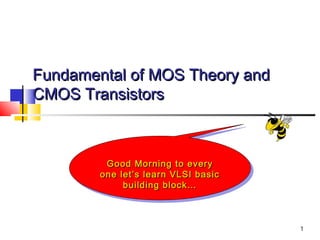
- 1. 1 Fundamental of MOS Theory andFundamental of MOS Theory and CMOS TransistorsCMOS Transistors Good Morning to everyGood Morning to every one let’s learn VLSI basicone let’s learn VLSI basic building block…building block… Good Morning to everyGood Morning to every one let’s learn VLSI basicone let’s learn VLSI basic building block…building block…
- 2. Prof.Kunal N Dekate, G H Raisoni college of Engineering Nagpur Basic Switch A pathpath exists when the Switch Control is closed If (Open) OUTPUT = unknown ; Switch is open (open (OFFOFF)) Else OUTPUT = INPUT ; Switch is closedclosed (ON) INPUT OUTPUT Switch Control
- 3. Prof.Kunal N Dekate, G H Raisoni college of Engineering Nagpur Semiconductors N+ N+ N- Al SiO2 Si X Y Conductivity of Si is proportional to No. of free carriers (electrons or “holes”) No. of free carriers is “programmable”: a. At fabrication time (N- means “small excess of electrons” N+ means “large excess of electrons”) b. At “run” time (heat/light/static charge/injection). edge view
- 4. Prof.Kunal N Dekate, G H Raisoni college of Engineering Nagpur MOS Transistor N+ N+ P- Al SiO2 Si X gate Y 1. The gate (metal) / SiO2 (oxide) / Si (semiconductor) sandwich makes a capacitor. 3. Result: a switch! 0V on gate -> OFF; +5V on gate -> ON + + + + + + + + + + + + + - - - - - - - - - - - - - 2. Charging the capacitor brings carriers to the surface of the oxide -- the carriers on the Si side make a high-conductivity channel.
- 5. Prof.Kunal N Dekate, G H Raisoni college of Engineering Nagpur The Analogy of A Transistor Cross SectionCross Section An N-Channel Metal-Oxide Semiconductor Field Effect Transistor (MOSFET) INPUT OUTPUT Switch Control (Gate)
- 6. Prof.Kunal N Dekate, G H Raisoni college of Engineering Nagpur NMOS Transistors 4 electrical terminals Source Drain Gate Substrate Connected to Gnd Source and drain are only different in their interpretation Terminal with lower voltage is the source (by convention) Simplified symbol omits the substrate DrainSource Gate Substrate (Body) VDVS VG
- 7. Prof.Kunal N Dekate, G H Raisoni college of Engineering Nagpur PMOS Transistors Same 4 electrical terminals Source Drain Gate Substrate Connected to VDD Again, source and drain are only different in their interpretation Terminal with higher voltage is the source (by convention) Simplified symbol omits the substrate Gate VDD Drain Source Substrate (Body) VG VDVS
- 8. Prof.Kunal N Dekate, G H Raisoni college of Engineering Nagpur Physical Structure of MOS FETS NMOS PMOS
- 9. Prof.Kunal N Dekate, G H Raisoni college of Engineering Nagpur Transistor Characteristics Cut-offCut-off Region Vgs – Vt ≤ 0 No current (Ids) between drain and source LinearLinear (or Ohmic) Region 0 < Vds < Vgs – Vt Ids is a function of Vgs and Vds Ids = β*[(Vgs-Vt)*Vds – Vds*Vds/2] SaturationSaturation Region 0 < Vgs – Vt < Vds Ids is independent of Vds Ids = (β/2)*(Vgs-Vt)2 β = process factor * (W/L) VtVt : Threshold voltage, a function of materials, doping, insulator thickness, etc. Gate Drain Source Ids Vds Vgs N-type MOS Transistor
- 10. 0 Prof.Kunal N Dekate, G H Raisoni college of Engineering Nagpur Transistor Characteristics
- 11. 1 Prof.Kunal N Dekate, G H Raisoni college of Engineering Nagpur MOS Capacitor Gate and body form MOS capacitor Operating modes Accumulation Depletion Inversion
- 12. 2 Prof.Kunal N Dekate, G H Raisoni college of Engineering Nagpur 3: CMOS Transistor Theory 12 Terminal Voltages Mode of operation depends on Vg, Vd, Vs Vgs = Vg – Vs Vgd = Vg – Vd Vds = Vd – Vs = Vgs - Vgd Source and drain are symmetric diffusion terminals By convention, source is terminal at lower voltage Hence Vds ≥ 0 nMOS body is grounded. First assume source is 0 too. Three regions of operation Cutoff Linear Saturation Vg Vs Vd Vgd Vgs Vds +- + - + -
- 13. 3 Prof.Kunal N Dekate, G H Raisoni college of Engineering Nagpur nMOS Cutoff No channel Ids ≈ 0 + - Vgs = 0 n+ n+ + - Vgd p-type body b g s d
- 14. 4 Prof.Kunal N Dekate, G H Raisoni college of Engineering Nagpur nMOS Linear Channel forms Current flows from d to s e- from s to d Ids increases with Vds Similar to linear resistor + - Vgs > Vt n+ n+ + - Vgd = Vgs + - Vgs > Vt n+ n+ + - Vgs > Vgd > Vt Vds = 0 0 < Vds < Vgs -Vt p-type body p-type body b g s d b g s d Ids
- 15. 5 Prof.Kunal N Dekate, G H Raisoni college of Engineering Nagpur Switches in Series INPUT OUTPUT S1 S2 Truth Table S1 S2 PATH? OFF OFF OFF ON ON OFF ON ON
- 16. 6 Prof.Kunal N Dekate, G H Raisoni college of Engineering Nagpur Switches in Series INPUT OUTPUT S1 S2 Truth Table (OFF/ON=0/1) S1 S2 PATH? OFF OFF NO OFF ON NO ON OFF NO ON ON YES What Function ??
- 17. 7 Prof.Kunal N Dekate, G H Raisoni college of Engineering Nagpur Switches in Series INPUT OUTPUT S1 S2 Truth Table (OFF/ON=0/1) S1 S2 PATH? 0 0 0 Function = ??
- 18. 8 Prof.Kunal N Dekate, G H Raisoni college of Engineering Nagpur Switches in Series INPUT OUTPUT S1 S2 Truth Table (OFF/ON=0/1) S1 S2 PATH? 0 0 0 0 1 0 Function = ??
- 19. 9 Prof.Kunal N Dekate, G H Raisoni college of Engineering Nagpur Switches in Series INPUT OUTPUT S1 S2 Truth Table (OFF/ON=0/1) S1 S2 PATH? 0 0 0 0 1 0 1 0 0 Function = ??
- 20. 0 Prof.Kunal N Dekate, G H Raisoni college of Engineering Nagpur Switches in Series INPUT OUTPUT S1 S2 Truth Table (OFF/ON=0/1) S1 S2 PATH? 0 0 0 0 1 0 1 0 0 1 1 1 Function = Logic ANDAND
- 21. 1 Prof.Kunal N Dekate, G H Raisoni college of Engineering Nagpur Switches in Parallel INPUT OUTPUT S1 Truth Table S1 S2 PATH? OFF OFF NO OFF ON YES ON OFF YES ON ON YES S2
- 22. 2 Prof.Kunal N Dekate, G H Raisoni college of Engineering Nagpur Switches in Parallel INPUT OUTPUT S1 Truth Table S1 S2 PATH? 0 0 0 Function =?? S2
- 23. 3 Prof.Kunal N Dekate, G H Raisoni college of Engineering Nagpur Switches in Parallel INPUT OUTPUT S1 Truth Table S1 S2 PATH? 0 0 0 0 1 1 Function =?? S2
- 24. 4 Prof.Kunal N Dekate, G H Raisoni college of Engineering Nagpur Switches in Parallel INPUT OUTPUT S1 Truth Table S1 S2 PATH? 0 0 0 0 1 1 1 0 1 Function =?? S2
- 25. 5 Prof.Kunal N Dekate, G H Raisoni college of Engineering Nagpur Switches in Parallel INPUT OUTPUT S1 Truth Table S1 S2 PATH? 0 0 0 0 1 1 1 0 1 1 1 1 Function = Logic OROR S2
- 26. 6 Prof.Kunal N Dekate, G H Raisoni college of Engineering Nagpur CMOS Transistor Complementary MOS P-channel MOS (pMOS) N-channel MOS (nMOS) pMOS P-type source and drain diffusions N substrate Mobility by holes nMOS N-type source and drain diffusions P substrate Mobility by electrons Gate Drain Source Gate Source Drain pMOS nMOS
- 27. 7 Prof.Kunal N Dekate, G H Raisoni college of Engineering Nagpur Pass Transistor using NMOS Assume capacitor (CL) is initially discharged Gate=1, Vin=1 CL begins to conduct and charges toward 1 (Vdd) and stops at (Vdd-Vt) Signal is degraded Gate=Vdd Vin=Vdd Vout Ground Load Capacitor Vgs I Gate=Vdd Vin=0 Vout=Vdd Ground Load Capacitor Vgs I Gate=1, Vin=0 CL begins to discharge toward 0
- 28. 8 Prof.Kunal N Dekate, G H Raisoni college of Engineering Nagpur Voltage Levels The binary values 0 and 1 can be represented as levels of current or of voltage voltage is most common Positive logic system associates 1 with high and 0 with low Max voltage is VDD (or VCC) 5V for TTL Much smaller (1.0 V) for ASICs Min voltage is VSS (or Gnd) Typically 0V Logic value 1 Undefined Logic value 0 Voltage VDD V1,min V0,max VSS (Gnd)
- 29. 9 Prof.Kunal N Dekate, G H Raisoni college of Engineering Nagpur Logic Ranges Typically V0,max = 0.4VDD and V1,min = 0.6VDD Logic value 1 Undefined Logic value 0 Voltage VDD V1,min V0,max VSS (Gnd) 5 V 3 V 2 V
- 30. 0 Prof.Kunal N Dekate, G H Raisoni college of Engineering Nagpur Transmission Degradation using Pass Transistor Vdd - VtVdd Vdd (1) Vdd - 2Vt Vdd Vdd Vdd Vout = Vdd- N*Vt Still 1??
- 31. 1 Prof.Kunal N Dekate, G H Raisoni college of Engineering Nagpur CMOS Signal Transfer Property Gate Path 0 Closed 1 Open Gate Drain Source Gate Source Drain Gate Path 0 Open 1 Closed pMOS nMOS • Transmits 1 well • Transmits 0 poorly • Transmits 0 well • Transmits 1 poorly
- 32. 2 Prof.Kunal N Dekate, G H Raisoni college of Engineering Nagpur CMOS Transmission Gate Transmit signal from INPUT to OUTPUT when Gate is closed Gate (complementary of Gatecomplementary of Gate) Source Drain Gate INPUT OUTPUT Gate pMOS nMOS OUTPUT 0 OFF OFF ZZ 1 ON ON INPUT ZZ : High-Impedance State, consider the terminal is “floating”
- 33. 3 Prof.Kunal N Dekate, G H Raisoni college of Engineering Nagpur High Impedance When a path exists Impedance is low to allow ample flow of current When no path Impedance is high allowing almost no current flow between two terminals Gate=1 DrainSource << 10KΩ >> 100MΩ Closed Gate=0 DrainSource Open
- 34. 4 Prof.Kunal N Dekate, G H Raisoni college of Engineering Nagpur Transmission Gates Gate = 1 0 0 Gate = 0 Transmit Logic 0 Gate = 1 1 1 Gate = 0 Transmit Logic 1
- 35. 5 Prof.Kunal N Dekate, G H Raisoni college of Engineering Nagpur Transmission Gate Symbol Gate Gate INPUT OUTPUT ≡≡
- 36. 6 Prof.Kunal N Dekate, G H Raisoni college of Engineering Nagpur CMOS Inverter Connect the following terminals of a PMOS and an NMOS Gates Drains Vin Vout Vdd Gnd Vout Vin Vin Vin = HIGH Vout = LOW (Gnd) ONON OFFOFF Vdd Gnd Vout Vin Vin Vin = LOW Vout = HIGH (Vdd) ONON OFFOFF Vdd PMOS Ground NMOS
- 37. 7 Prof.Kunal N Dekate, G H Raisoni college of Engineering Nagpur CMOS Voltage Transfer Characteristics Vdd Gnd Vin Vout PMOS NMOS OFF: V_GateToSource < V_Threshold LINEAR (or OHMIC): 0< V_DrainToSource < V_GateToSource - V_Threshold SATURATION: 0 < V_GateToSource - V_Threshold < V_DrainToSource Note that in the CMOS Inverter → V_GateToSource = V_in
- 38. 8 Prof.Kunal N Dekate, G H Raisoni college of Engineering Nagpur Pull-Up and Pull-Down Network CMOS network consists of a Pull- UP Network (PUN) and a Pull- Down Network (PDN) PUN consists of a set of PMOS transistors PDN consists of a set of NMOS transistors PUN and PDN implementations are complimentary to each other PMOS ↔ NOMS Series topology ↔ Parallel topology …. I0 I1 In-1 OUPTUT Vdd PUN Gnd PDN
- 39. 9 Prof.Kunal N Dekate, G H Raisoni college of Engineering Nagpur PUN/PDN of a CMOS Inverter A B 0 1 1 Z A B 0 Z 1 0 A B 0 1 1 0 Pull-Up Network Pull-Down Network Combined CMOS Network Vdd A Gnd B CMOS Inverter
- 40. 0 Prof.Kunal N Dekate, G H Raisoni college of Engineering Nagpur Gate Symbol of a CMOS Inverter Vdd A Gnd B CMOS Inverter A B B = Ā
- 41. 1 Prof.Kunal N Dekate, G H Raisoni college of Engineering Nagpur PUN/PDN of a NAND Gate A B C 0 0 1 0 1 1 1 0 1 1 1 Z A B C 0 0 Z 0 1 Z 1 0 Z 1 1 0 Pull-Up Network Pull-Down Network Vdd A B A B C
- 42. 2 Prof.Kunal N Dekate, G H Raisoni college of Engineering Nagpur PUN/PDN of a NAND Gate A B C 0 0 1 0 1 1 1 0 1 1 1 Z A B C 0 0 Z 0 1 Z 1 0 Z 1 1 0 A B C 0 0 1 0 1 1 1 0 1 1 1 0 Pull-Up Network Pull-Down Network Combined CMOS Network Vdd A B A B C
- 43. 3 Prof.Kunal N Dekate, G H Raisoni college of Engineering Nagpur NAND Gate Symbol A B C 0 0 1 0 1 1 1 0 1 1 1 0 Vdd A B A B C A B C Truth Table BAC ⋅=
- 44. 4 Prof.Kunal N Dekate, G H Raisoni college of Engineering Nagpur PUN/PDN of a NOR Gate A B C 0 0 1 0 1 Z 1 0 Z 1 1 Z A B C 0 0 Z 0 1 0 1 0 0 1 1 0 Pull-Up Network Pull-Down Network Vdd A C B A B
- 45. 5 Prof.Kunal N Dekate, G H Raisoni college of Engineering Nagpur PUN/PDN of a NOR Gate A B C 0 0 1 0 1 Z 1 0 Z 1 1 Z A B C 0 0 Z 0 1 0 1 0 0 1 1 0 A B C 0 0 1 0 1 0 1 0 0 1 1 0 Pull-Up Network Pull-Down Network Combined CMOS Network A C B A B Vdd
- 46. 6 Prof.Kunal N Dekate, G H Raisoni college of Engineering Nagpur NOR Gate Symbol A B C 0 0 1 0 1 0 1 0 0 1 1 0 A B C Truth Table A C B A B BAC += Vdd
- 47. 7 Prof.Kunal N Dekate, G H Raisoni college of Engineering Nagpur How about an AND gate Vdd A B A Vdd Gnd C NAN D Inverter B C = A B A B C
- 48. 8 Prof.Kunal N Dekate, G H Raisoni college of Engineering Nagpur An OR Gate A B A B Vdd Vdd Gnd C Inverter NOR A B C BAC +=
- 49. 9 Prof.Kunal N Dekate, G H Raisoni college of Engineering Nagpur What’s the Function of the following CMOS Network? Vdd A B A A A B B B C A B C 0 0 Z 0 1 1 1 0 1 1 1 Z A B C 0 0 0 0 1 Z 1 0 Z 1 1 0 A B C 0 0 0 0 1 1 1 0 1 1 1 0 Pull-Up Network Pull-Down Network Combined CMOS Network Function = XORXOR
- 50. 0 Prof.Kunal N Dekate, G H Raisoni college of Engineering Nagpur Yet Another XOR CMOS Network Vdd A B A A A B B B C A B C 0 0 Z 0 1 1 1 0 1 1 1 Z A B C 0 0 0 0 1 Z 1 0 Z 1 1 0 A B C 0 0 0 0 1 1 1 0 1 1 1 0 Pull-Up Network Pull-Down Network Combined CMOS Network Function = XORXOR
- 51. 1 Prof.Kunal N Dekate, G H Raisoni college of Engineering Nagpur Exclusive-OR (XOR) Gate Vdd A B A A A B B B C A B C 0 0 0 0 1 1 1 0 1 1 1 0 A B C Truth Table BABABAC ⊕=⋅+⋅=
- 52. 2 Prof.Kunal N Dekate, G H Raisoni college of Engineering Nagpur How about XNORXNOR Gate A B C 0 0 1 0 1 0 1 0 0 1 1 1 A B C Truth Table BABABAC ⊕=⋅+⋅= How do we draw the corresponding CMOS network given a Boolean equation?
- 53. 3 Prof.Kunal N Dekate, G H Raisoni college of Engineering Nagpur How about XNORXNOR Gate A B C 0 0 1 0 1 0 1 0 0 1 1 1 A B C Truth Table BABAC ⋅+⋅= Vdd A B A A A B B B C Vdd XOR Inverter
- 54. 4 Prof.Kunal N Dekate, G H Raisoni college of Engineering Nagpur A Systematic Approach Each variable in the given Boolean eqn corresponds to a PMOS transistor in PUN and an NMOS transistor in PDN Draw PUNPUN using PMOS based on the Boolean eqn ANDAND operation drawn in seriesseries OROR operation drawn in parallelparallel Invert each variablevariable of the Boolean eqn as the gate input for each PMOS in the PUN Draw PDNPDN using NMOS in complementary form Parallel (PUN) to series (PDN) Series (PUN) to parallel (PDN) Label with the same inputs of PUN Label the output
- 55. 5 Prof.Kunal N Dekate, G H Raisoni college of Engineering Nagpur Example 1 BCAF +⋅= In series In parallel Vdd (1) Draw the Pull-Up Network
- 56. 6 Prof.Kunal N Dekate, G H Raisoni college of Engineering Nagpur Example 1 BCAF +⋅= In series In parallel Vdd (2) Assign the complemented input A C B
- 57. 7 Prof.Kunal N Dekate, G H Raisoni college of Engineering Nagpur Example 1 BCAF +⋅= In series In parallel Vdd (3) Draw the Pull-Down Network in the complementary form A C B A C
- 58. 8 Prof.Kunal N Dekate, G H Raisoni college of Engineering Nagpur Example 1 BCAF +⋅= In series In parallel Vdd (3) Draw the Pull-Down Network in the complementary form A C B A C B
- 59. 9 Prof.Kunal N Dekate, G H Raisoni college of Engineering Nagpur Example 1 BCAF +⋅= In series In parallel Vdd Label the output F A C B A C B F
- 60. 0 Prof.Kunal N Dekate, G H Raisoni college of Engineering Nagpur Example 1 BCAF +⋅= In series In parallel Vdd A C B A C B F A B C F 0 0 0 0 0 0 1 0 0 1 0 1 0 1 1 1 1 0 0 1 1 0 1 0 1 1 0 1 1 1 1 1 Truth Table
- 61. 1 Prof.Kunal N Dekate, G H Raisoni college of Engineering Nagpur An Alternative for XNOR Gate A B C 0 0 1 0 1 0 1 0 0 1 1 1 A B C Truth Table BABAC ⋅+⋅= Vdd A B A B A A B B C
- 62. 2 Prof.Kunal N Dekate, G H Raisoni college of Engineering Nagpur Example 3 )C(ABDAF +⋅+⋅= Start from the innermost term A B D AC A D
- 63. 3 Prof.Kunal N Dekate, G H Raisoni college of Engineering Nagpur Example 3 )C(ABDAF +⋅+⋅= Start from the innermost term A B D AC A D A C
- 64. 4 Prof.Kunal N Dekate, G H Raisoni college of Engineering Nagpur Example 3 )C(ABDAF +⋅+⋅= Start from the innermost term A B D AC A D A C B
- 65. 5 Prof.Kunal N Dekate, G H Raisoni college of Engineering Nagpur Example 3 )C(ABDAF +⋅+⋅= Start from the innermost term A B D AC A D A C B Vdd F Pull-Up Network Pull-Down Network
- 66. 6 Prof.Kunal N Dekate, G H Raisoni college of Engineering Nagpur Example 4 ))C(ABDA()D(EF +⋅+⋅⋅+= Start from the innermost term A B D AC A D A C B Vdd F E D E D Pull-Down Network Pull-Up Network
- 67. 7 Prof.Kunal N Dekate, G H Raisoni college of Engineering Nagpur Another Example BCAF +⋅= How ??
- 68. 8 Prof.Kunal N Dekate, G H Raisoni college of Engineering Nagpur Performance 1: Gate Delay X (Input) Y (Output) Delay proportional to R * C R (on resistance of the driver) C (gate capacitance of the receiver) X Y
- 69. 9 Prof.Kunal N Dekate, G H Raisoni college of Engineering Nagpur Minimum unit of delay: tau = R * C N+ N+ P Al SiO2 Si X gate Y Top view Edge view L W R proportional to L/W. (typical: 10Kohms) C proportional to W * L (typical: 10fF) L & W quantized to multiples of the “minimum line width”, currently 0.13um
- 70. 0 Prof.Kunal N Dekate, G H Raisoni college of Engineering Nagpur Gate Delay Minimum delay (“tau”) assumes minimum- size transistors Additional delay arises from fanout real-world outputs (pins ~1pF +) long wires... Can increase driving transistor width (W) to reduce delay. note exponential chain.
- 71. 1 Prof.Kunal N Dekate, G H Raisoni college of Engineering Nagpur Performance 2: Wire Delay X (Input) Y (Output) Delay proportional to R * C R (on resistance PLUS wire resistance) C (gate capacitance PLUS wire capacitance) X Y
- 72. 2 Prof.Kunal N Dekate, G H Raisoni college of Engineering Nagpur Reference: Prof. Hsien-Hsin Sean Lee Lecture Notes Introduction to Computer Engg. School of Electrical and Computer Engineering. Georgia Institute of Technology