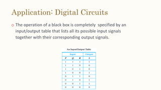
Download to read offline

![Application of Propositional Logic
o Propositional logic can be applied to the design of computer
hardware.
o A logic circuit (or digital circuit) receives input signals p1, p2, .
. . , pn, each a bit [either 0 (off) or 1 (on)], and produces
output signals s1, s2, . . . , sn, each a bit.
– Because of variety of digital circuits think basic circuits
black boxes.](https://image.slidesharecdn.com/constructingcircuitsforbooleanexpressionsgate-151126140459-lva1-app6891/85/Constructing-circuits-for-boolean-expressions-gate-2-320.jpg)

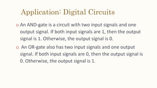
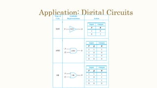
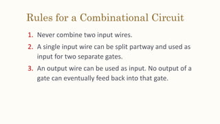


This document discusses the application of propositional logic to digital circuits. It describes how digital circuits use basic logic gates like NOT, AND and OR gates to process input signals and produce output signals. Complicated digital circuits can be constructed by combining these basic gates. The document also provides rules for building combinational circuits and techniques for simplifying circuits, such as constructing truth tables and using Boolean algebraic identities.


