Downloaded 1,423 times
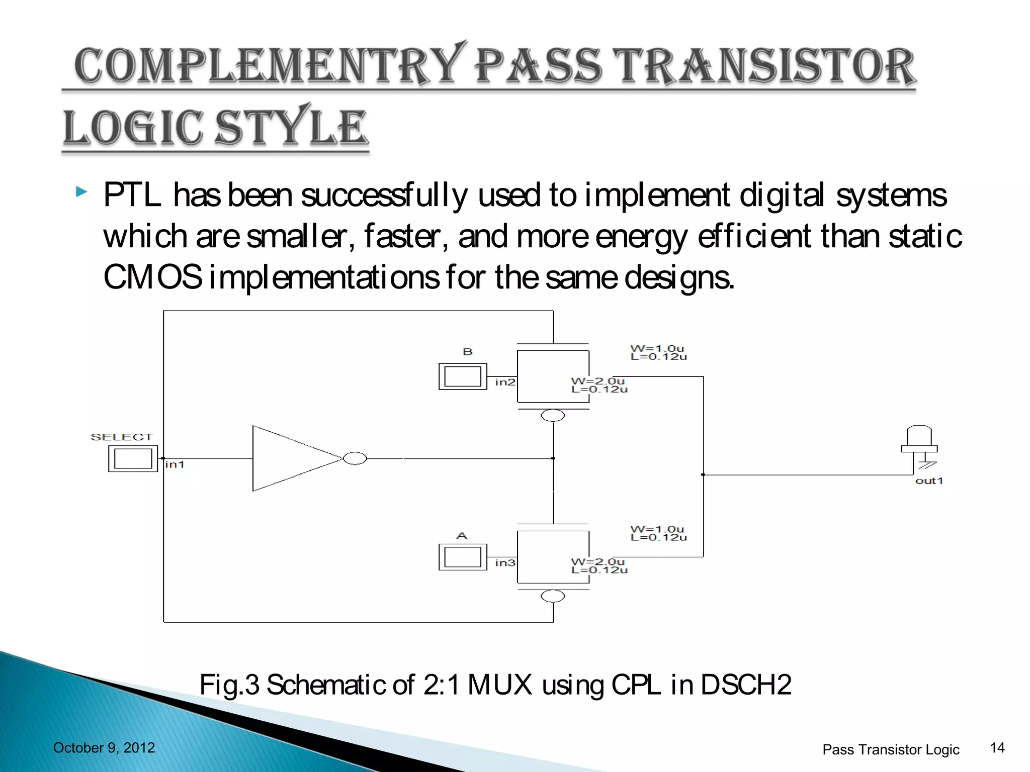
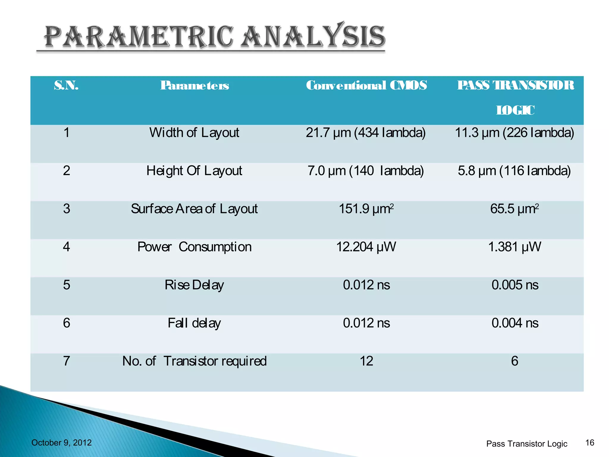


This document compares the use of complementary pass-transistor logic (CPL) to conventional CMOS design. CPL uses fewer transistors than CMOS gates, has smaller capacitances, and is faster. A 2:1 multiplexer is designed using both CMOS and CPL in Microwind and DSCH2 layout tools. Simulation results show the CPL multiplexer has lower power consumption, smaller area, faster rise/fall delays compared to the CMOS multiplexer. Therefore, CPL offers advantages over conventional CMOS in terms of speed, area, and power-delay products.
Introduction by Diwaker Pant on Pass Transistor Logic, its advantages over CMOS, lab work, and conclusions.
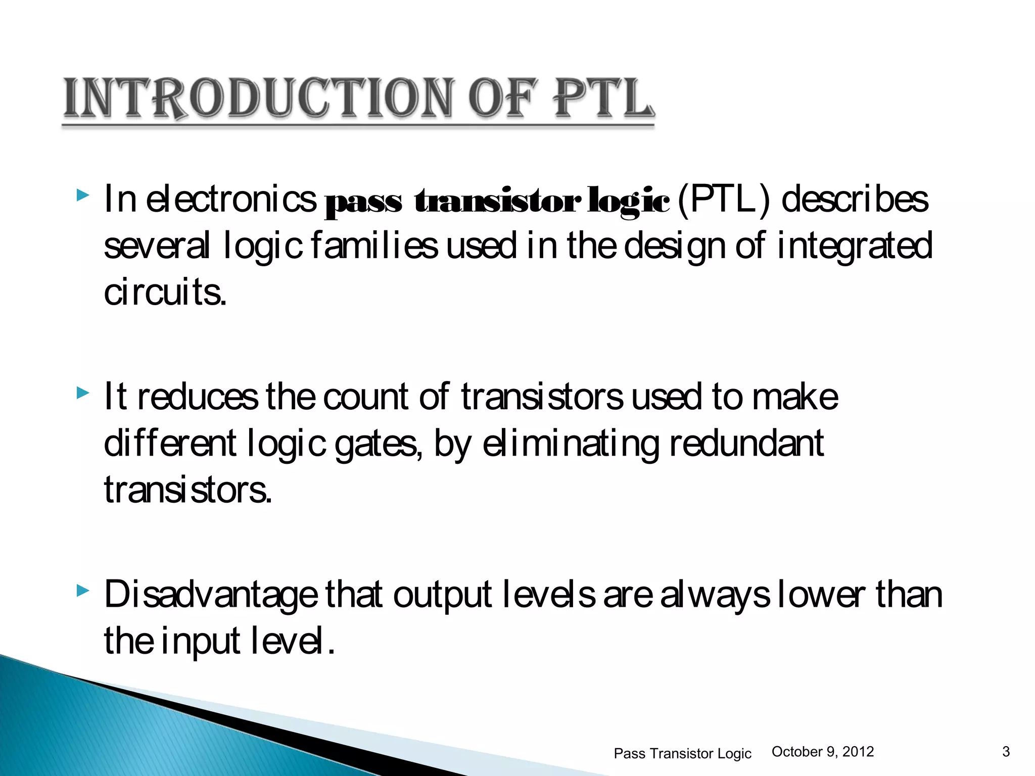
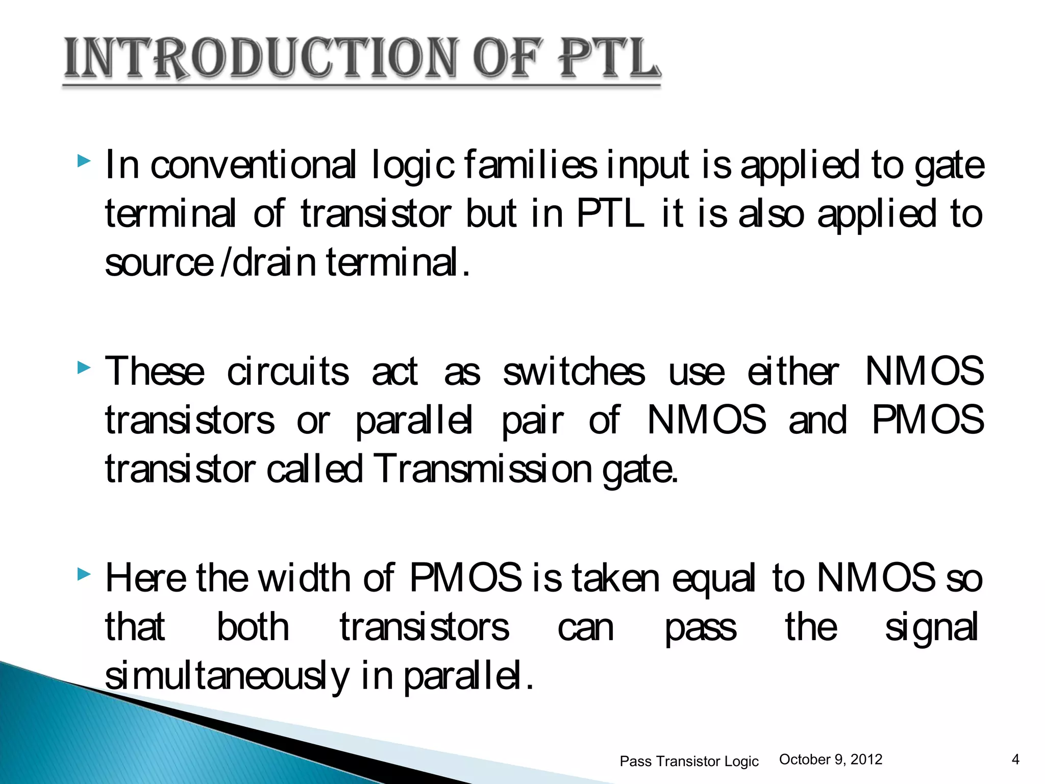
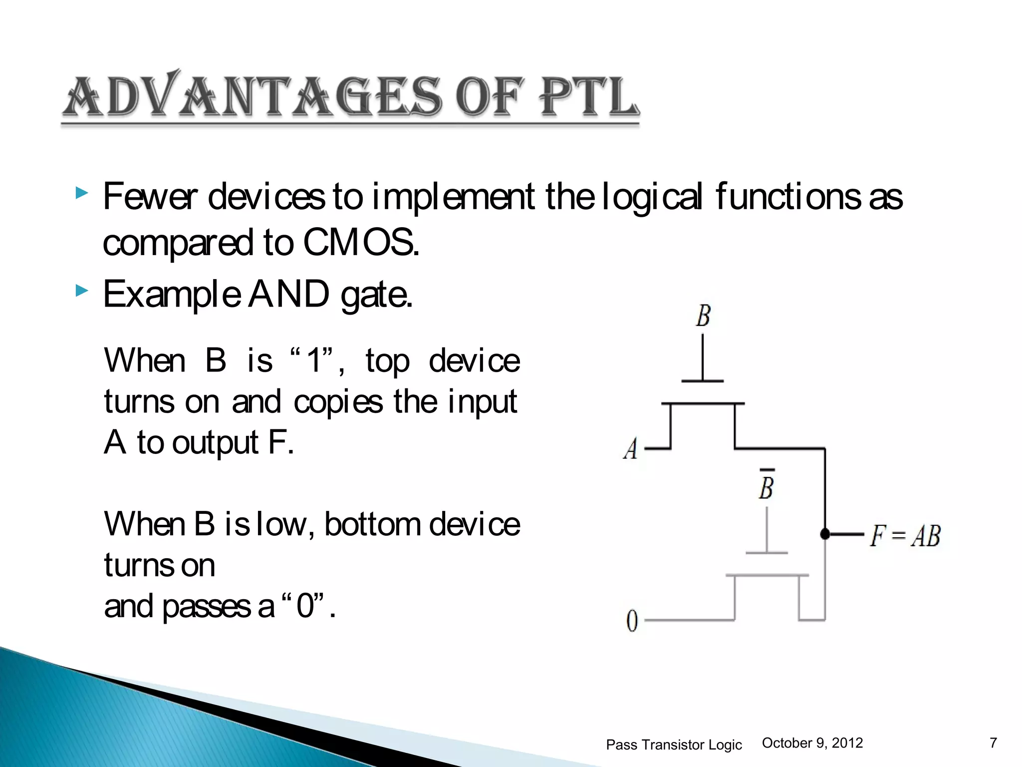
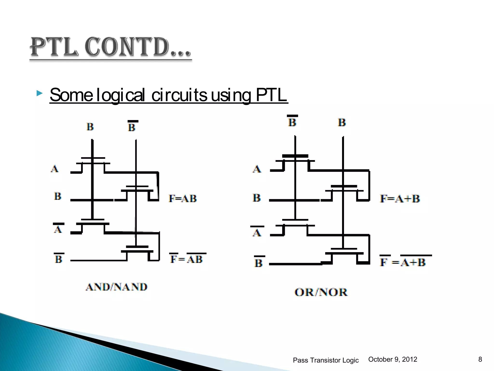
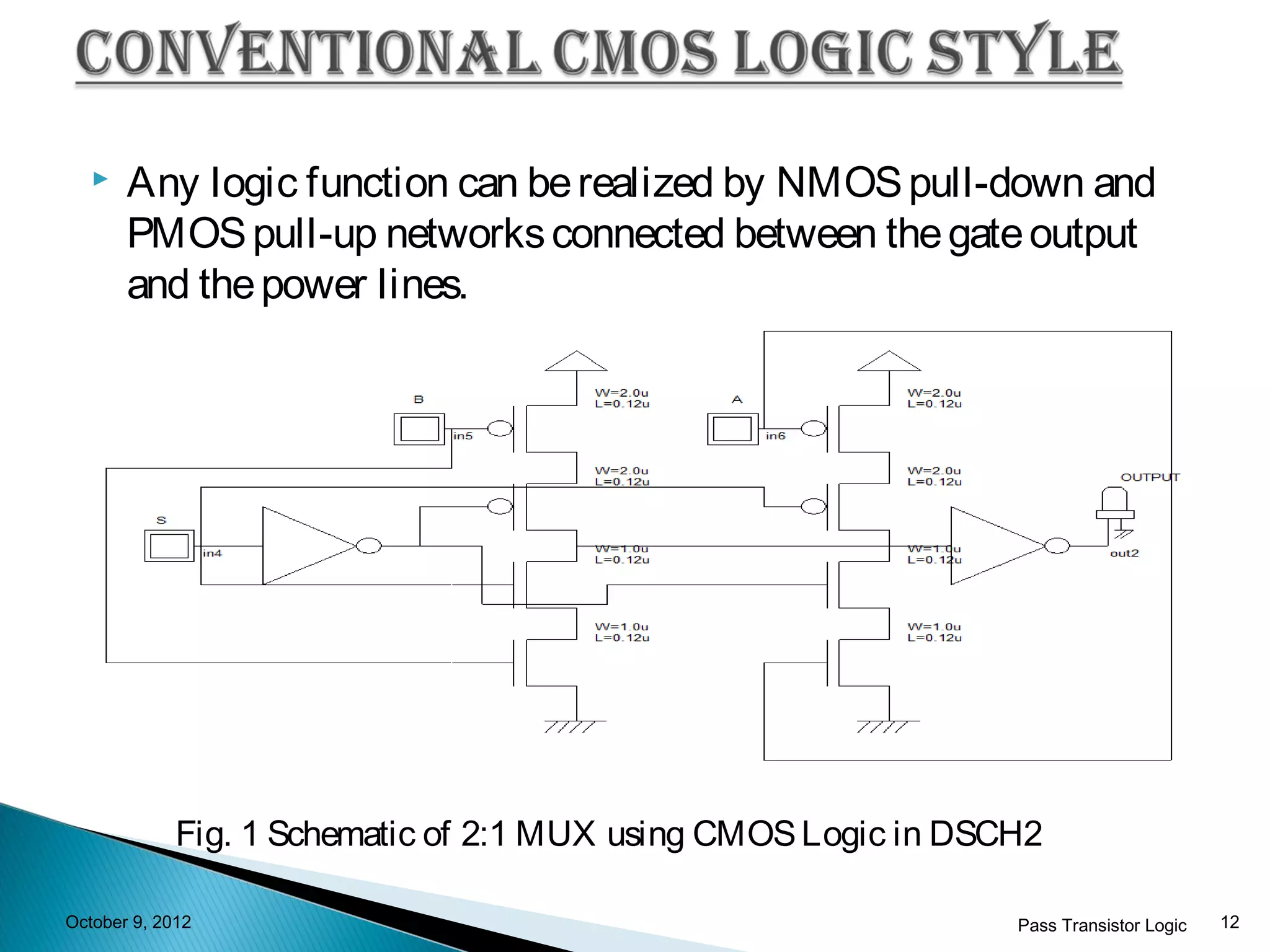
PTL reduces transistor count compared to CMOS, operating principles using NMOS/PMOS, and the performance characteristics of PTL.
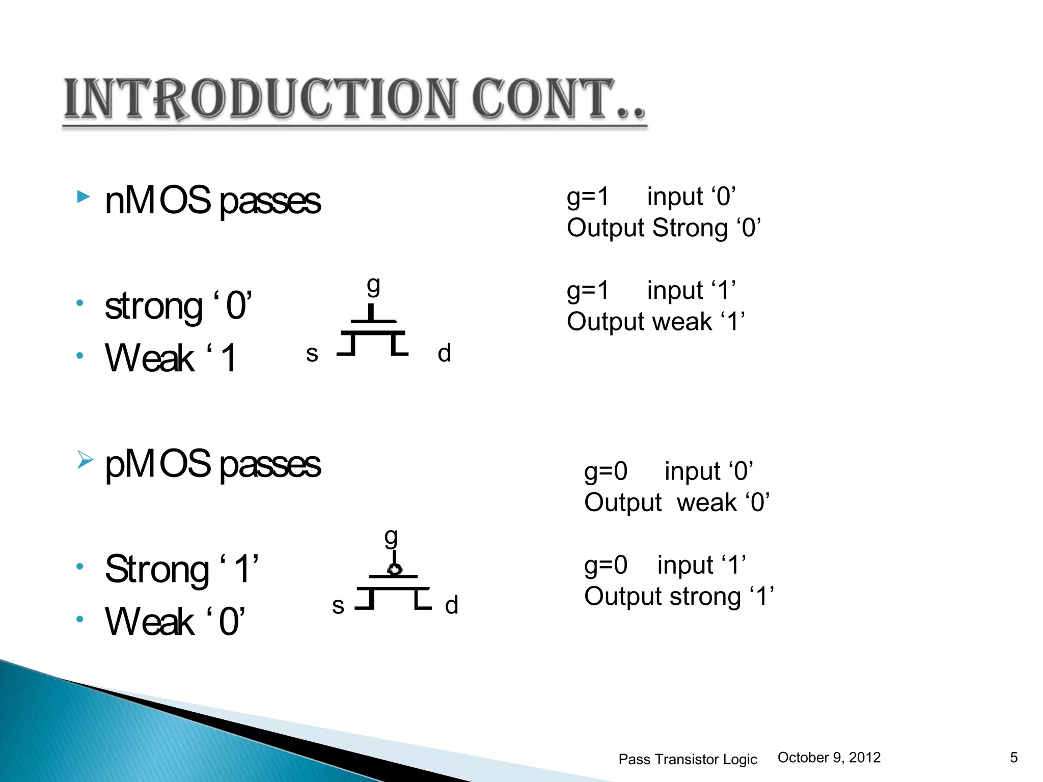
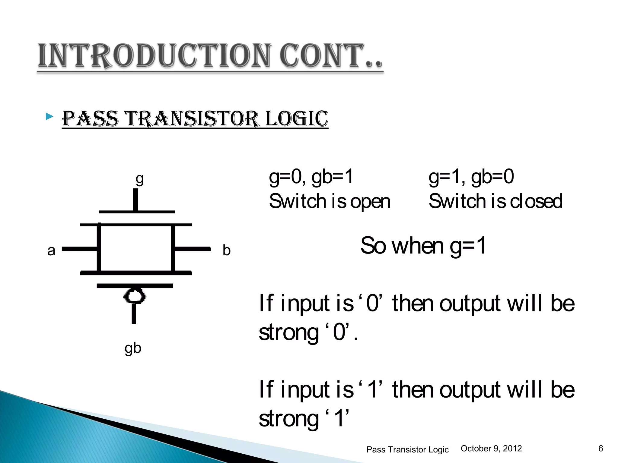
PTL's operation analyzed with examples, including AND gate implementation and how NMOS/PMOS transistors affect output levels and signal strength.
CPL is more power-efficient than conventional CMOS. Discusses design comparisons using a 2:1 multiplexer in Microwind and DSCH2 tools.
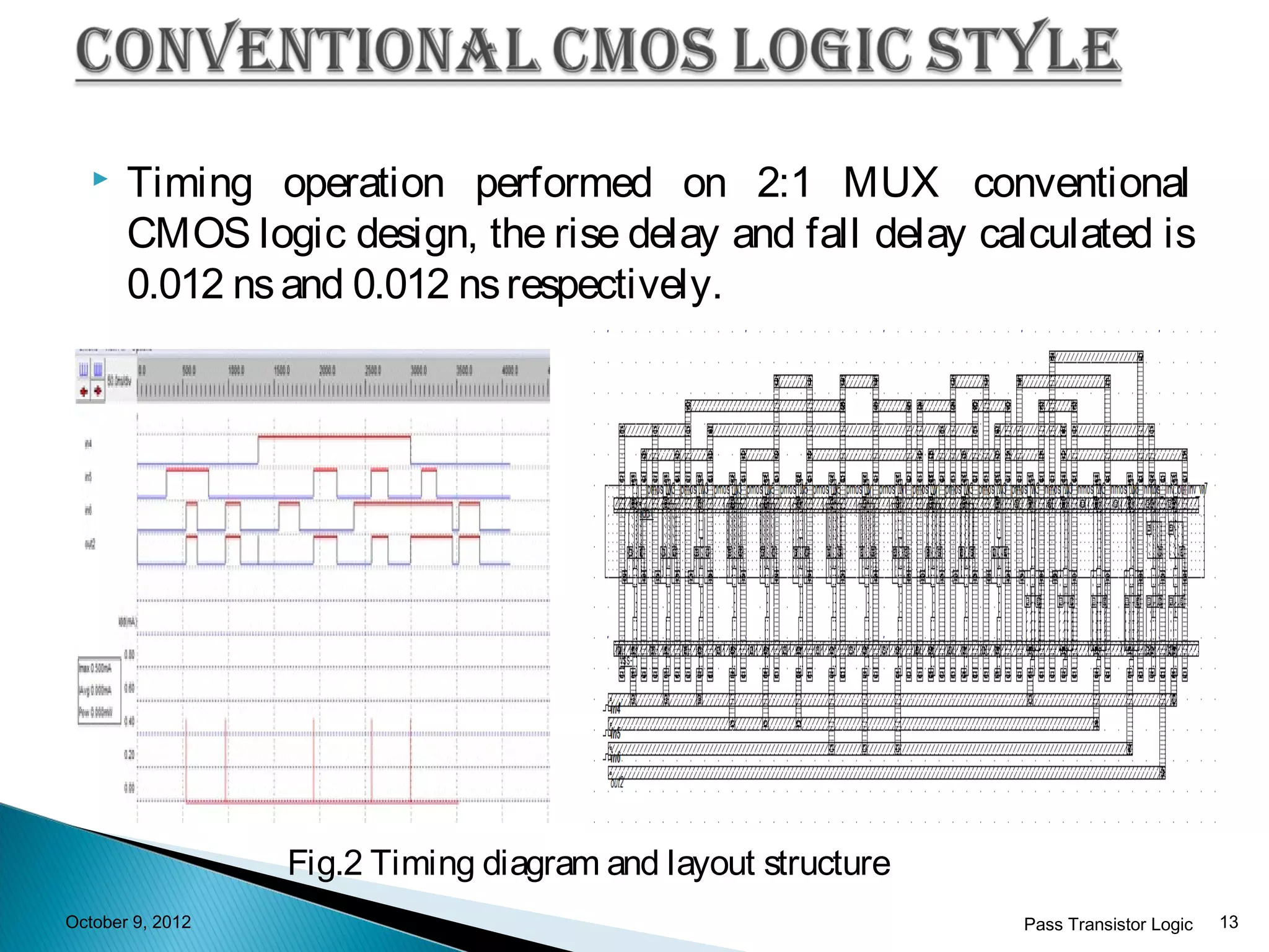
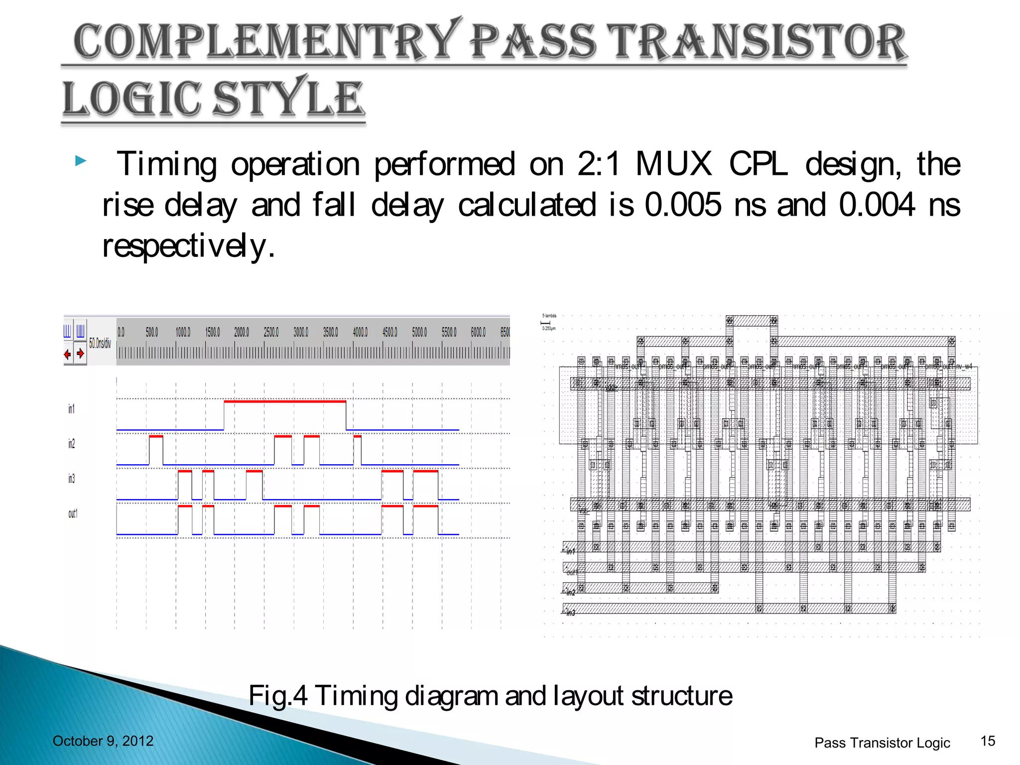
Timing analysis of 2:1 MUX designs, detailing rise and fall delays, layout parameters, and power consumption of PTL compared to CMOS.
List of resources and papers referenced in the study of Pass Transistor Logic and CMOS design.