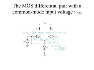
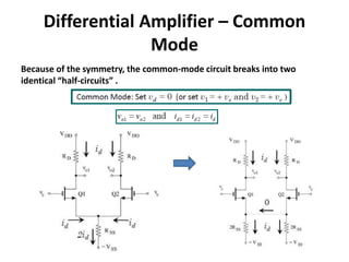
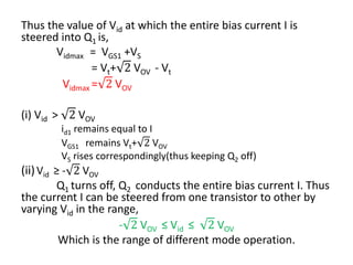
The document discusses the design and operation of a MOSFET differential amplifier, detailing its input and output signals, regions of operation, and common-mode rejection capabilities. It explains the equations governing drain current, overdrive voltage, and the implications of common-mode and differential modes of operation. Additionally, it highlights the advantages and disadvantages of using differential amplifiers in various applications, including analog systems and audio amplifiers.


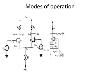
![Regions of operation
• Cut off region- VGS ≤ Vt
• Active region- VDS ≤ VOV
• Saturation region- VDS ≥ VOV
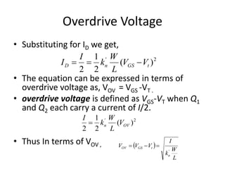
TO DERIVE DRAIN CURRENT EQUATION
|Q|/unit channel length = Cox W VOV
Drift velocity= μn|E|= μn (VDS/L)
The drain current is the product of charge per unit length and drift velocity
ID=[( μnCox)(W/L) VOV] VDS
ID=[( μnCox)(W/L) VGS-Vt] VDS
ID=[kn’(W/L) VGS-Vt] VDS
Replacing VOV by (VOV-(1/2) VDS)
ID=kn’(W/L) (VOV-(1/2) VDS) VDS
At saturation mode, VDS ≥ VOV,
ID=(1/2) kn’(W/L)V2
OV](https://image.slidesharecdn.com/mos-170622151906/85/DIFFERENTIAL-AMPLIFIER-using-MOSFET-6-320.jpg)