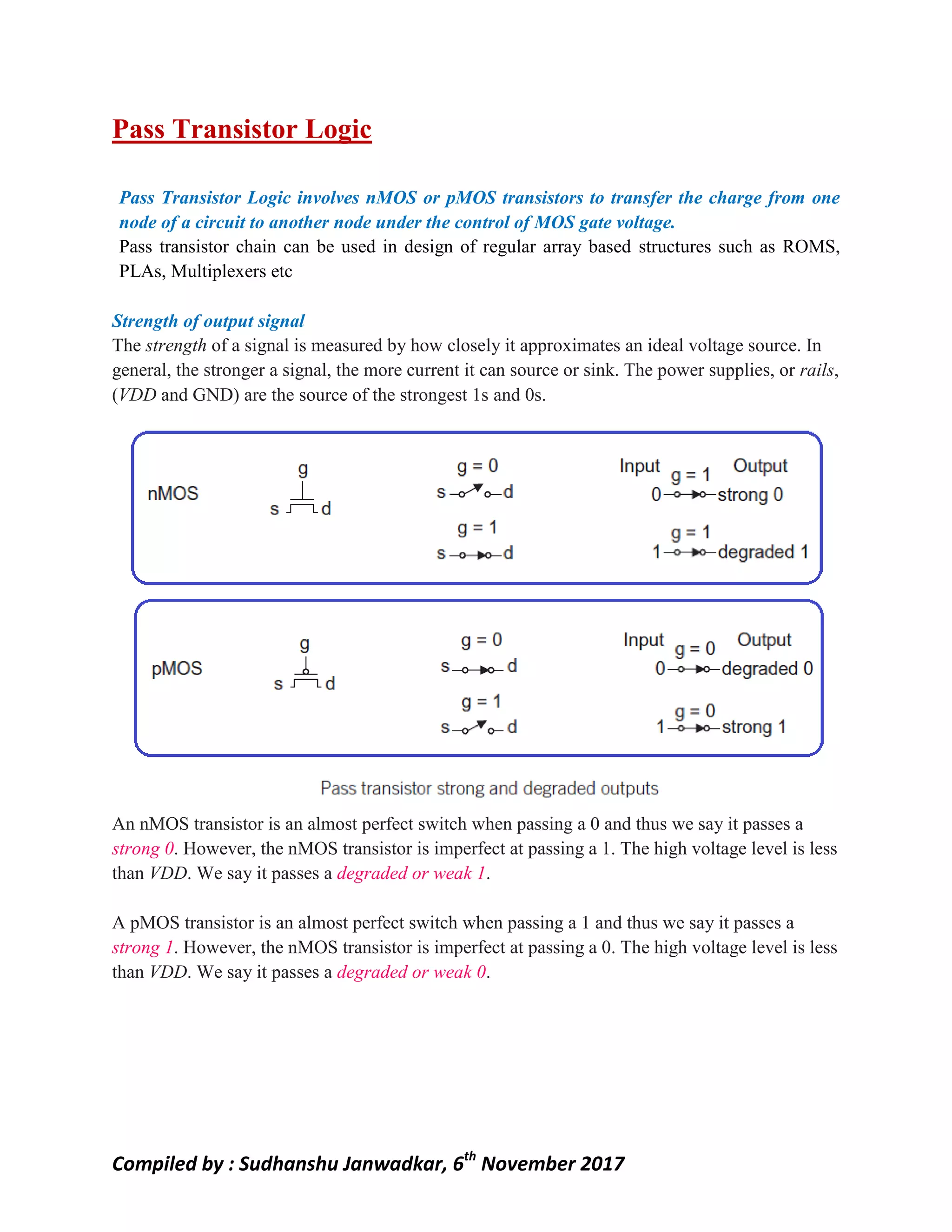
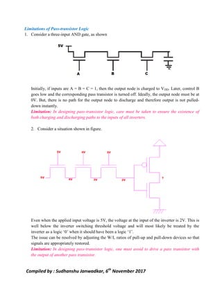
SlideShare a Scribd company logo
Compiled by : Sudhanshu Janwadkar, 6th
November 2017
Pass Transistor Logic
Pass Transistor Logic involves nMOS or pMOS transistors to transfer the charge from one
node of a circuit to another node under the control of MOS gate voltage.
Pass transistor chain can be used in design of regular array based structures such as ROMS,
PLAs, Multiplexers etc
Strength of output signal
The strength of a signal is measured by how closely it approximates an ideal voltage source. In
general, the stronger a signal, the more current it can source or sink. The power supplies, or rails,
(VDD and GND) are the source of the strongest 1s and 0s.
An nMOS transistor is an almost perfect switch when passing a 0 and thus we say it passes a
strong 0. However, the nMOS transistor is imperfect at passing a 1. The high voltage level is less
than VDD. We say it passes a degraded or weak 1.
A pMOS transistor is an almost perfect switch when passing a 1 and thus we say it passes a
strong 1. However, the nMOS transistor is imperfect at passing a 0. The high voltage level is less
than VDD. We say it passes a degraded or weak 0.
Compiled by : Sudhanshu Janwadkar, 6th
November 2017
Threshold Drops
Rule 1. If the Gate and Drain are both at VDD, the source can rise only upto one threshold
below the gate. If the Source tries to rise higher, the device goes to Cut-off region.
Compiled by : Sudhanshu Janwadkar, 6th
November 2017
Rule 2. If the Gate is at-least one threshold voltage higher than the drain, the source will
rise within few millivolts to Drain potential.
Rule 3. If the Gate and Drain of a pass-transistor are both High, the source will rise to the
lower of the two potentials VDD and VG-VT.
Thus, following generalization can be made.
Compiled by : Sudhanshu Janwadkar, 6th
November 2017
Exercises:
Compiled by : Sudhanshu Janwadkar, 6th
November 2017
Exercises:
Advantages of Pass-transistor Logic
1. They are not ratio-ed devices and hence, minimum geometry transistor can be used
2. They do not dissipate stand-by power.
3. They utilize the minimum number of transistors to implement a logic function.
Compiled by : Sudhanshu Janwadkar, 6th
November 2017
Limitations of Pass-transistor Logic
1. Consider a three-input AND gate, as shown
Initially, if inputs are A = B = C = 1, then the output node is charged to VDD. Later, control B
goes low and the corresponding pass transistor is turned off. Ideally, the output node must be at
0V. But, there is no path for the output node to discharge and therefore output is not pulled-
down instantly.
Limitation: In designing pass-transistor logic, care must be taken to ensure the existence of
both charging and discharging paths to the inputs of all inverters.
2. Consider a situation shown in figure.
Even when the applied input voltage is 5V, the voltage at the input of the inverter is 2V. This is
well below the inverter switching threshold voltage and will most likely be treated by the
inverter as a logic ‘0’ when it should have been a logic ‘1’.
The issue can be resolved by adjusting the W/L ratios of pull-up and pull-down devices so that
signals are appropriately restored.
Limitation: In designing pass-transistor logic, one must avoid to drive a pass transistor with
the output of another pass transistor.
Compiled by : Sudhanshu Janwadkar, 6th
November 2017
3. Charge sharing
Charge sharing problems occur when two capacitive nodes charged to different voltages are
connected through a pass-transistor. When the pass transistor is turned on, it connects the two
nodes, resulting in redistribution of the charge on both nodes.
Charge sharing is a serious problem in pre-charge circuits and must be carefully guarded
against.
4. Sneak paths
A sneak path is created when two pass transistors are both ON at the same time and one is
connected to VDD while the other os connected to GND.
Charge Sharing
Capacitors C1 and C2 are in parallel when pass transistor P is conducting. This forces the
voltages across C1 and C2 to be equal. If the two capacitors are charged to different initial
voltages, charge sharing will occur when P turns on.
Let the initial voltage and charge on C1 be V1 and Q1, and the initial voltage and charge on C2 be
V2 and Q2. After the pass transistor turns on, the final charges on C1 and C2 are Q1f and Q2f,
respectively, and both capacitors are charged to voltage Vf.
Compiled by : Sudhanshu Janwadkar, 6th
November 2017
The initial charge balance equation is
Q1 + Q2 = C1V1 +C2V2
The final charge balance equation is
Q1f + Q2f = (C1 +C2)Vf
To find the final charge distribution, equate the charges before and after P turns on
C1V1 + C2V2 = (C1 +C2) Vf
Solve for Vf, then Q1f
Vf =
C1V1+C2V2
C1+C2
Q1f = C1Vf = (C1V1 +C2 V2) (
C1
C1+C2
)
Exercise:
Determine the charge on each capacitor of figure above, before and after P turns on, if C1=20fF,
C2=20fF, V1= 1V and V2 =5V.
Solution:
Initially, Q1 =C1V1 =20fC, and Q2 = C2V2 = 100fC.
After P turns on,
Vf =
20 1 + 20(5)
20+20
= 30V
Q1f = Q2f =C1Vf = 20(3) = 60fC.
Compiled by : Sudhanshu Janwadkar, 6th
November 2017
Try it yourself
1. Determine the charge on each capactor before and after P turns on, if C1 =10fF, C2 =50fF,
V1 =0V, V2 = 5V and VG = 6V.
2. Repeat 1 if, C1 is 2.6fF and C2 is 4fF.
Designing Pass Transistor Logic Circuits
The following circuit shows a General function block to realize Boolean Gates using pass
transistor logic, such that both charging and discharging paths exist.
I0 and I1 are the control inputs to be applied at Drain Terminal and C0 and C1 are the gate control
inputs.
Output Inputs Controls
Y I0 I1 C0 C1
AB 0 B A’ A
(AB)’ 1 B’ A’ A
A +B B 1 A’ A
(A + B)’ B’ 0 A’ A
A ^ B B B’ A’ A
(A ^ B)’ B’ B A’ A
Multiplexer A B S’ S
Compiled by : Sudhanshu Janwadkar, 6th
November 2017
Try it yourself:
1. The output of a majority gate is true if at least two inputs are true. The controls are A and
B. Show the Karnaugh map. Design a pass-transistor circuit for a three-input majority gate.
2. Design a pass-transistor circuit for a 2:4 decoder.
3. Realize the following gates using Pass transistor logic:
a. 3-input NAND gate
b. 3-input NOR gate
c. 3-input XOR gate
d. 3-input XNOR gate

More Related Content

What's hot

Rc delay modelling in vlsi
Rc delay modelling in vlsiRc delay modelling in vlsi
Rc delay modelling in vlsi
Dr. Vishal Sharma
 
Chap16-1-NMOS-Inverter.pdf
Chap16-1-NMOS-Inverter.pdfChap16-1-NMOS-Inverter.pdf
Chap16-1-NMOS-Inverter.pdf
ahmedsalim244821
 
Second order effects
Second order effectsSecond order effects
Second order effects
PRAVEEN KUMAR CHITLURI
 
optimazation of standard cell layout
optimazation of standard cell layoutoptimazation of standard cell layout
optimazation of standard cell layoutE ER Yash nagaria
 
WPE
WPEWPE
Dynamic logic circuits
Dynamic logic circuitsDynamic logic circuits
Dynamic logic circuits
Kalyan Kumar Kalita
 
VLSI
VLSIVLSI
CMOS LOGIC STRUCTURES
CMOS LOGIC STRUCTURESCMOS LOGIC STRUCTURES
CMOS LOGIC STRUCTURES
VaishaliVaishali14
 
Regions of operation of bjt and mosfet
Regions of operation of bjt and mosfetRegions of operation of bjt and mosfet
Regions of operation of bjt and mosfet
MahoneyKadir
 
Switch level modeling
Switch level modelingSwitch level modeling
Switch level modeling
Devi Pradeep Podugu
 
CMOS Topic 6 -_designing_combinational_logic_circuits
CMOS Topic 6 -_designing_combinational_logic_circuitsCMOS Topic 6 -_designing_combinational_logic_circuits
CMOS Topic 6 -_designing_combinational_logic_circuits
Ikhwan_Fakrudin
 
Channel length Modulation
Channel length ModulationChannel length Modulation
Channel length Modulation
Engineering Funda
 
Mos transistor
Mos transistorMos transistor
Mos transistor
Murali Rai
 
CMOS Logic
CMOS LogicCMOS Logic
CMOS Inverter static characterstics.pptx
CMOS Inverter static characterstics.pptxCMOS Inverter static characterstics.pptx
CMOS Inverter static characterstics.pptx
indrajeetPatel22
 
Short Channel Effect In MOSFET
Short Channel Effect In MOSFETShort Channel Effect In MOSFET
Short Channel Effect In MOSFET
Sudhanshu Srivastava
 
mos transistor
mos transistormos transistor
mos transistor
harshalprajapati78
 

What's hot (20)

Rc delay modelling in vlsi
Rc delay modelling in vlsiRc delay modelling in vlsi
Rc delay modelling in vlsi
 
Chap16-1-NMOS-Inverter.pdf
Chap16-1-NMOS-Inverter.pdfChap16-1-NMOS-Inverter.pdf
Chap16-1-NMOS-Inverter.pdf
 
Pass transistor logic
Pass transistor logicPass transistor logic
Pass transistor logic
 
Second order effects
Second order effectsSecond order effects
Second order effects
 
optimazation of standard cell layout
optimazation of standard cell layoutoptimazation of standard cell layout
optimazation of standard cell layout
 
WPE
WPEWPE
WPE
 
Comparator
ComparatorComparator
Comparator
 
Dynamic logic circuits
Dynamic logic circuitsDynamic logic circuits
Dynamic logic circuits
 
VLSI
VLSIVLSI
VLSI
 
Lecture20
Lecture20Lecture20
Lecture20
 
CMOS LOGIC STRUCTURES
CMOS LOGIC STRUCTURESCMOS LOGIC STRUCTURES
CMOS LOGIC STRUCTURES
 
Regions of operation of bjt and mosfet
Regions of operation of bjt and mosfetRegions of operation of bjt and mosfet
Regions of operation of bjt and mosfet
 
Switch level modeling
Switch level modelingSwitch level modeling
Switch level modeling
 
CMOS Topic 6 -_designing_combinational_logic_circuits
CMOS Topic 6 -_designing_combinational_logic_circuitsCMOS Topic 6 -_designing_combinational_logic_circuits
CMOS Topic 6 -_designing_combinational_logic_circuits
 
Channel length Modulation
Channel length ModulationChannel length Modulation
Channel length Modulation
 
Mos transistor
Mos transistorMos transistor
Mos transistor
 
CMOS Logic
CMOS LogicCMOS Logic
CMOS Logic
 
CMOS Inverter static characterstics.pptx
CMOS Inverter static characterstics.pptxCMOS Inverter static characterstics.pptx
CMOS Inverter static characterstics.pptx
 
Short Channel Effect In MOSFET
Short Channel Effect In MOSFETShort Channel Effect In MOSFET
Short Channel Effect In MOSFET
 
mos transistor
mos transistormos transistor
mos transistor
 

Similar to Pass Transistor Logic

vlsi 2 unit.pdfvlsi unit 2 important notes for ece department
vlsi 2 unit.pdfvlsi unit 2 important notes for ece departmentvlsi 2 unit.pdfvlsi unit 2 important notes for ece department
vlsi 2 unit.pdfvlsi unit 2 important notes for ece department
nitcse
 
Thyristors (2)
Thyristors (2)Thyristors (2)
Thyristors (2)Chethan Sp
 
Introduction to scr thyristers
Introduction to scr thyristersIntroduction to scr thyristers
Introduction to scr thyristers
iqtadar ali gilani
 
Thyristor Characteristics, Two Transistor Model Of Thyristor & Thyrisror Turn...
Thyristor Characteristics, Two Transistor Model Of Thyristor & Thyrisror Turn...Thyristor Characteristics, Two Transistor Model Of Thyristor & Thyrisror Turn...
Thyristor Characteristics, Two Transistor Model Of Thyristor & Thyrisror Turn...
University of Gujrat, Pakistan
 
Diodes vi characteries
Diodes vi characteriesDiodes vi characteries
Diodes vi characteries
Manikandan Chinnadurai
 
CMOS logic circuits
CMOS logic circuitsCMOS logic circuits
CMOS logic circuits
Mahesh_Naidu
 
VLSIM3.pptx
VLSIM3.pptxVLSIM3.pptx
VLSIM3.pptx
savithaj5
 
Ch03updated
Ch03updatedCh03updated
Ch03updated
Muhammad Saad
 
VLSI- Unit II
VLSI- Unit IIVLSI- Unit II
VLSI- Unit II
MADHUMITHA154
 
Cmos logic
Cmos logicCmos logic
Ppt 2
Ppt 2Ppt 2
Diode Clampers
Diode ClampersDiode Clampers
Diode Clampers
DoCircuits
 
cmoslogic_data7.pdf
cmoslogic_data7.pdfcmoslogic_data7.pdf
cmoslogic_data7.pdf
kalivaraprasad2
 
Fed vonverter project design and progress report
Fed vonverter project design and progress reportFed vonverter project design and progress report
Fed vonverter project design and progress report
MehboobUET
 
Clippers AND Clampers
Clippers AND ClampersClippers AND Clampers
Clippers AND Clampers
JUNAID SK
 
Fundamentals of CMOS VLSI Design and Mos Transistors
Fundamentals of CMOS VLSI Design and Mos TransistorsFundamentals of CMOS VLSI Design and Mos Transistors
Fundamentals of CMOS VLSI Design and Mos Transistors
srknec
 
Pccoe basic mobile_robot
Pccoe basic mobile_robotPccoe basic mobile_robot
Pccoe basic mobile_robotAjendra Joshi
 
G43064245
G43064245G43064245
G43064245
IJERA Editor
 
Oscillators
OscillatorsOscillators
Oscillators
12nitin
 

Similar to Pass Transistor Logic (20)

vlsi 2 unit.pdfvlsi unit 2 important notes for ece department
vlsi 2 unit.pdfvlsi unit 2 important notes for ece departmentvlsi 2 unit.pdfvlsi unit 2 important notes for ece department
vlsi 2 unit.pdfvlsi unit 2 important notes for ece department
 
Thyristors (2)
Thyristors (2)Thyristors (2)
Thyristors (2)
 
Introduction to scr thyristers
Introduction to scr thyristersIntroduction to scr thyristers
Introduction to scr thyristers
 
Thyristor Characteristics, Two Transistor Model Of Thyristor & Thyrisror Turn...
Thyristor Characteristics, Two Transistor Model Of Thyristor & Thyrisror Turn...Thyristor Characteristics, Two Transistor Model Of Thyristor & Thyrisror Turn...
Thyristor Characteristics, Two Transistor Model Of Thyristor & Thyrisror Turn...
 
Diodes vi characteries
Diodes vi characteriesDiodes vi characteries
Diodes vi characteries
 
CMOS logic circuits
CMOS logic circuitsCMOS logic circuits
CMOS logic circuits
 
VLSIM3.pptx
VLSIM3.pptxVLSIM3.pptx
VLSIM3.pptx
 
Ch03updated
Ch03updatedCh03updated
Ch03updated
 
VLSI- Unit II
VLSI- Unit IIVLSI- Unit II
VLSI- Unit II
 
Cmos logic
Cmos logicCmos logic
Cmos logic
 
Ppt 2
Ppt 2Ppt 2
Ppt 2
 
Diode Clampers
Diode ClampersDiode Clampers
Diode Clampers
 
cmoslogic_data7.pdf
cmoslogic_data7.pdfcmoslogic_data7.pdf
cmoslogic_data7.pdf
 
Fed vonverter project design and progress report
Fed vonverter project design and progress reportFed vonverter project design and progress report
Fed vonverter project design and progress report
 
Clippers AND Clampers
Clippers AND ClampersClippers AND Clampers
Clippers AND Clampers
 
Lec-4.pdf
Lec-4.pdfLec-4.pdf
Lec-4.pdf
 
Fundamentals of CMOS VLSI Design and Mos Transistors
Fundamentals of CMOS VLSI Design and Mos TransistorsFundamentals of CMOS VLSI Design and Mos Transistors
Fundamentals of CMOS VLSI Design and Mos Transistors
 
Pccoe basic mobile_robot
Pccoe basic mobile_robotPccoe basic mobile_robot
Pccoe basic mobile_robot
 
G43064245
G43064245G43064245
G43064245
 
Oscillators
OscillatorsOscillators
Oscillators
 

More from Sudhanshu Janwadkar

DSP Processors versus ASICs
DSP Processors versus ASICsDSP Processors versus ASICs
DSP Processors versus ASICs
Sudhanshu Janwadkar
 
Keypad Interfacing with 8051 Microcontroller
Keypad Interfacing with 8051 MicrocontrollerKeypad Interfacing with 8051 Microcontroller
Keypad Interfacing with 8051 Microcontroller
Sudhanshu Janwadkar
 
ASIC design Flow (Digital Design)
ASIC design Flow (Digital Design)ASIC design Flow (Digital Design)
ASIC design Flow (Digital Design)
Sudhanshu Janwadkar
 
Fpga architectures and applications
Fpga architectures and applicationsFpga architectures and applications
Fpga architectures and applications
Sudhanshu Janwadkar
 
LCD Interacing with 8051
LCD Interacing with 8051LCD Interacing with 8051
LCD Interacing with 8051
Sudhanshu Janwadkar
 
Interrupts in 8051
Interrupts in 8051Interrupts in 8051
Interrupts in 8051
Sudhanshu Janwadkar
 
Serial Communication in 8051
Serial Communication in 8051Serial Communication in 8051
Serial Communication in 8051
Sudhanshu Janwadkar
 
SPI Bus Protocol
SPI Bus ProtocolSPI Bus Protocol
SPI Bus Protocol
Sudhanshu Janwadkar
 
I2C Protocol
I2C ProtocolI2C Protocol
I2C Protocol
Sudhanshu Janwadkar
 
Introduction to 8051 Timer/Counter
Introduction to 8051 Timer/CounterIntroduction to 8051 Timer/Counter
Introduction to 8051 Timer/Counter
Sudhanshu Janwadkar
 
Intel 8051 Programming in C
Intel 8051 Programming in CIntel 8051 Programming in C
Intel 8051 Programming in C
Sudhanshu Janwadkar
 
Hardware View of Intel 8051
Hardware View of Intel 8051Hardware View of Intel 8051
Hardware View of Intel 8051
Sudhanshu Janwadkar
 
Architecture of the Intel 8051 Microcontroller
Architecture of the Intel 8051 MicrocontrollerArchitecture of the Intel 8051 Microcontroller
Architecture of the Intel 8051 Microcontroller
Sudhanshu Janwadkar
 
Introduction to Embedded Systems
Introduction to Embedded SystemsIntroduction to Embedded Systems
Introduction to Embedded Systems
Sudhanshu Janwadkar
 
Interconnects in Reconfigurable Architectures
Interconnects in Reconfigurable ArchitecturesInterconnects in Reconfigurable Architectures
Interconnects in Reconfigurable Architectures
Sudhanshu Janwadkar
 
Introduction to FPGAs
Introduction to FPGAsIntroduction to FPGAs
Introduction to FPGAs
Sudhanshu Janwadkar
 
Design and Implementation of a GPS based Personal Tracking System
Design and Implementation of a GPS based Personal Tracking SystemDesign and Implementation of a GPS based Personal Tracking System
Design and Implementation of a GPS based Personal Tracking System
Sudhanshu Janwadkar
 
Embedded Logic Flip-Flops: A Conceptual Review
Embedded Logic Flip-Flops: A Conceptual ReviewEmbedded Logic Flip-Flops: A Conceptual Review
Embedded Logic Flip-Flops: A Conceptual Review
Sudhanshu Janwadkar
 
Memory and Processor Testing
Memory and Processor TestingMemory and Processor Testing
Memory and Processor Testing
Sudhanshu Janwadkar
 
Silicon on Insulator (SOI) Technology
Silicon on Insulator (SOI) TechnologySilicon on Insulator (SOI) Technology
Silicon on Insulator (SOI) Technology
Sudhanshu Janwadkar
 

More from Sudhanshu Janwadkar (20)

DSP Processors versus ASICs
DSP Processors versus ASICsDSP Processors versus ASICs
DSP Processors versus ASICs
 
Keypad Interfacing with 8051 Microcontroller
Keypad Interfacing with 8051 MicrocontrollerKeypad Interfacing with 8051 Microcontroller
Keypad Interfacing with 8051 Microcontroller
 
ASIC design Flow (Digital Design)
ASIC design Flow (Digital Design)ASIC design Flow (Digital Design)
ASIC design Flow (Digital Design)
 
Fpga architectures and applications
Fpga architectures and applicationsFpga architectures and applications
Fpga architectures and applications
 
LCD Interacing with 8051
LCD Interacing with 8051LCD Interacing with 8051
LCD Interacing with 8051
 
Interrupts in 8051
Interrupts in 8051Interrupts in 8051
Interrupts in 8051
 
Serial Communication in 8051
Serial Communication in 8051Serial Communication in 8051
Serial Communication in 8051
 
SPI Bus Protocol
SPI Bus ProtocolSPI Bus Protocol
SPI Bus Protocol
 
I2C Protocol
I2C ProtocolI2C Protocol
I2C Protocol
 
Introduction to 8051 Timer/Counter
Introduction to 8051 Timer/CounterIntroduction to 8051 Timer/Counter
Introduction to 8051 Timer/Counter
 
Intel 8051 Programming in C
Intel 8051 Programming in CIntel 8051 Programming in C
Intel 8051 Programming in C
 
Hardware View of Intel 8051
Hardware View of Intel 8051Hardware View of Intel 8051
Hardware View of Intel 8051
 
Architecture of the Intel 8051 Microcontroller
Architecture of the Intel 8051 MicrocontrollerArchitecture of the Intel 8051 Microcontroller
Architecture of the Intel 8051 Microcontroller
 
Introduction to Embedded Systems
Introduction to Embedded SystemsIntroduction to Embedded Systems
Introduction to Embedded Systems
 
Interconnects in Reconfigurable Architectures
Interconnects in Reconfigurable ArchitecturesInterconnects in Reconfigurable Architectures
Interconnects in Reconfigurable Architectures
 
Introduction to FPGAs
Introduction to FPGAsIntroduction to FPGAs
Introduction to FPGAs
 
Design and Implementation of a GPS based Personal Tracking System
Design and Implementation of a GPS based Personal Tracking SystemDesign and Implementation of a GPS based Personal Tracking System
Design and Implementation of a GPS based Personal Tracking System
 
Embedded Logic Flip-Flops: A Conceptual Review
Embedded Logic Flip-Flops: A Conceptual ReviewEmbedded Logic Flip-Flops: A Conceptual Review
Embedded Logic Flip-Flops: A Conceptual Review
 
Memory and Processor Testing
Memory and Processor TestingMemory and Processor Testing
Memory and Processor Testing
 
Silicon on Insulator (SOI) Technology
Silicon on Insulator (SOI) TechnologySilicon on Insulator (SOI) Technology
Silicon on Insulator (SOI) Technology
 

Recently uploaded

Overview on Edible Vaccine: Pros & Cons with Mechanism
Overview on Edible Vaccine: Pros & Cons with MechanismOverview on Edible Vaccine: Pros & Cons with Mechanism
Overview on Edible Vaccine: Pros & Cons with Mechanism
DeeptiGupta154
 
Model Attribute Check Company Auto Property
Model Attribute  Check Company Auto PropertyModel Attribute  Check Company Auto Property
Model Attribute Check Company Auto Property
Celine George
 
Introduction to AI for Nonprofits with Tapp Network
Introduction to AI for Nonprofits with Tapp NetworkIntroduction to AI for Nonprofits with Tapp Network
Introduction to AI for Nonprofits with Tapp Network
TechSoup
 
Chapter -12, Antibiotics (One Page Notes).pdf
Chapter -12, Antibiotics (One Page Notes).pdfChapter -12, Antibiotics (One Page Notes).pdf
Chapter -12, Antibiotics (One Page Notes).pdf
Kartik Tiwari
 
A Strategic Approach: GenAI in Education
A Strategic Approach: GenAI in EducationA Strategic Approach: GenAI in Education
A Strategic Approach: GenAI in Education
Peter Windle
 
The approach at University of Liverpool.pptx
The approach at University of Liverpool.pptxThe approach at University of Liverpool.pptx
The approach at University of Liverpool.pptx
Jisc
 
STRAND 3 HYGIENIC PRACTICES.pptx GRADE 7 CBC
STRAND 3 HYGIENIC PRACTICES.pptx GRADE 7 CBCSTRAND 3 HYGIENIC PRACTICES.pptx GRADE 7 CBC
STRAND 3 HYGIENIC PRACTICES.pptx GRADE 7 CBC
kimdan468
 
The Diamond Necklace by Guy De Maupassant.pptx
The Diamond Necklace by Guy De Maupassant.pptxThe Diamond Necklace by Guy De Maupassant.pptx
The Diamond Necklace by Guy De Maupassant.pptx
DhatriParmar
 
Lapbook sobre os Regimes Totalitários.pdf
Lapbook sobre os Regimes Totalitários.pdfLapbook sobre os Regimes Totalitários.pdf
Lapbook sobre os Regimes Totalitários.pdf
Jean Carlos Nunes Paixão
 
Synthetic Fiber Construction in lab .pptx
Synthetic Fiber Construction in lab .pptxSynthetic Fiber Construction in lab .pptx
Synthetic Fiber Construction in lab .pptx
Pavel ( NSTU)
 
A Survey of Techniques for Maximizing LLM Performance.pptx
A Survey of Techniques for Maximizing LLM Performance.pptxA Survey of Techniques for Maximizing LLM Performance.pptx
A Survey of Techniques for Maximizing LLM Performance.pptx
thanhdowork
 
1.4 modern child centered education - mahatma gandhi-2.pptx
1.4 modern child centered education - mahatma gandhi-2.pptx1.4 modern child centered education - mahatma gandhi-2.pptx
1.4 modern child centered education - mahatma gandhi-2.pptx
JosvitaDsouza2
 
Digital Tools and AI for Teaching Learning and Research
Digital Tools and AI for Teaching Learning and ResearchDigital Tools and AI for Teaching Learning and Research
Digital Tools and AI for Teaching Learning and Research
Vikramjit Singh
 
The basics of sentences session 5pptx.pptx
The basics of sentences session 5pptx.pptxThe basics of sentences session 5pptx.pptx
The basics of sentences session 5pptx.pptx
heathfieldcps1
 
June 3, 2024 Anti-Semitism Letter Sent to MIT President Kornbluth and MIT Cor...
June 3, 2024 Anti-Semitism Letter Sent to MIT President Kornbluth and MIT Cor...June 3, 2024 Anti-Semitism Letter Sent to MIT President Kornbluth and MIT Cor...
June 3, 2024 Anti-Semitism Letter Sent to MIT President Kornbluth and MIT Cor...
Levi Shapiro
 
Marketing internship report file for MBA
Marketing internship report file for MBAMarketing internship report file for MBA
Marketing internship report file for MBA
gb193092
 
Chapter 3 - Islamic Banking Products and Services.pptx
Chapter 3 - Islamic Banking Products and Services.pptxChapter 3 - Islamic Banking Products and Services.pptx
Chapter 3 - Islamic Banking Products and Services.pptx
Mohd Adib Abd Muin, Senior Lecturer at Universiti Utara Malaysia
 
Guidance_and_Counselling.pdf B.Ed. 4th Semester
Guidance_and_Counselling.pdf B.Ed. 4th SemesterGuidance_and_Counselling.pdf B.Ed. 4th Semester
Guidance_and_Counselling.pdf B.Ed. 4th Semester
Atul Kumar Singh
 
CACJapan - GROUP Presentation 1- Wk 4.pdf
CACJapan - GROUP Presentation 1- Wk 4.pdfCACJapan - GROUP Presentation 1- Wk 4.pdf
CACJapan - GROUP Presentation 1- Wk 4.pdf
camakaiclarkmusic
 
Digital Artifact 2 - Investigating Pavilion Designs
Digital Artifact 2 - Investigating Pavilion DesignsDigital Artifact 2 - Investigating Pavilion Designs
Digital Artifact 2 - Investigating Pavilion Designs
chanes7
 

Recently uploaded (20)

Overview on Edible Vaccine: Pros & Cons with Mechanism
Overview on Edible Vaccine: Pros & Cons with MechanismOverview on Edible Vaccine: Pros & Cons with Mechanism
Overview on Edible Vaccine: Pros & Cons with Mechanism
 
Model Attribute Check Company Auto Property
Model Attribute  Check Company Auto PropertyModel Attribute  Check Company Auto Property
Model Attribute Check Company Auto Property
 
Introduction to AI for Nonprofits with Tapp Network
Introduction to AI for Nonprofits with Tapp NetworkIntroduction to AI for Nonprofits with Tapp Network
Introduction to AI for Nonprofits with Tapp Network
 
Chapter -12, Antibiotics (One Page Notes).pdf
Chapter -12, Antibiotics (One Page Notes).pdfChapter -12, Antibiotics (One Page Notes).pdf
Chapter -12, Antibiotics (One Page Notes).pdf
 
A Strategic Approach: GenAI in Education
A Strategic Approach: GenAI in EducationA Strategic Approach: GenAI in Education
A Strategic Approach: GenAI in Education
 
The approach at University of Liverpool.pptx
The approach at University of Liverpool.pptxThe approach at University of Liverpool.pptx
The approach at University of Liverpool.pptx
 
STRAND 3 HYGIENIC PRACTICES.pptx GRADE 7 CBC
STRAND 3 HYGIENIC PRACTICES.pptx GRADE 7 CBCSTRAND 3 HYGIENIC PRACTICES.pptx GRADE 7 CBC
STRAND 3 HYGIENIC PRACTICES.pptx GRADE 7 CBC
 
The Diamond Necklace by Guy De Maupassant.pptx
The Diamond Necklace by Guy De Maupassant.pptxThe Diamond Necklace by Guy De Maupassant.pptx
The Diamond Necklace by Guy De Maupassant.pptx
 
Lapbook sobre os Regimes Totalitários.pdf
Lapbook sobre os Regimes Totalitários.pdfLapbook sobre os Regimes Totalitários.pdf
Lapbook sobre os Regimes Totalitários.pdf
 
Synthetic Fiber Construction in lab .pptx
Synthetic Fiber Construction in lab .pptxSynthetic Fiber Construction in lab .pptx
Synthetic Fiber Construction in lab .pptx
 
A Survey of Techniques for Maximizing LLM Performance.pptx
A Survey of Techniques for Maximizing LLM Performance.pptxA Survey of Techniques for Maximizing LLM Performance.pptx
A Survey of Techniques for Maximizing LLM Performance.pptx
 
1.4 modern child centered education - mahatma gandhi-2.pptx
1.4 modern child centered education - mahatma gandhi-2.pptx1.4 modern child centered education - mahatma gandhi-2.pptx
1.4 modern child centered education - mahatma gandhi-2.pptx
 
Digital Tools and AI for Teaching Learning and Research
Digital Tools and AI for Teaching Learning and ResearchDigital Tools and AI for Teaching Learning and Research
Digital Tools and AI for Teaching Learning and Research
 
The basics of sentences session 5pptx.pptx
The basics of sentences session 5pptx.pptxThe basics of sentences session 5pptx.pptx
The basics of sentences session 5pptx.pptx
 
June 3, 2024 Anti-Semitism Letter Sent to MIT President Kornbluth and MIT Cor...
June 3, 2024 Anti-Semitism Letter Sent to MIT President Kornbluth and MIT Cor...June 3, 2024 Anti-Semitism Letter Sent to MIT President Kornbluth and MIT Cor...
June 3, 2024 Anti-Semitism Letter Sent to MIT President Kornbluth and MIT Cor...
 
Marketing internship report file for MBA
Marketing internship report file for MBAMarketing internship report file for MBA
Marketing internship report file for MBA
 
Chapter 3 - Islamic Banking Products and Services.pptx
Chapter 3 - Islamic Banking Products and Services.pptxChapter 3 - Islamic Banking Products and Services.pptx
Chapter 3 - Islamic Banking Products and Services.pptx
 
Guidance_and_Counselling.pdf B.Ed. 4th Semester
Guidance_and_Counselling.pdf B.Ed. 4th SemesterGuidance_and_Counselling.pdf B.Ed. 4th Semester
Guidance_and_Counselling.pdf B.Ed. 4th Semester
 
CACJapan - GROUP Presentation 1- Wk 4.pdf
CACJapan - GROUP Presentation 1- Wk 4.pdfCACJapan - GROUP Presentation 1- Wk 4.pdf
CACJapan - GROUP Presentation 1- Wk 4.pdf
 
Digital Artifact 2 - Investigating Pavilion Designs
Digital Artifact 2 - Investigating Pavilion DesignsDigital Artifact 2 - Investigating Pavilion Designs
Digital Artifact 2 - Investigating Pavilion Designs
 

Pass Transistor Logic

  • 1. Compiled by : Sudhanshu Janwadkar, 6th November 2017 Pass Transistor Logic Pass Transistor Logic involves nMOS or pMOS transistors to transfer the charge from one node of a circuit to another node under the control of MOS gate voltage. Pass transistor chain can be used in design of regular array based structures such as ROMS, PLAs, Multiplexers etc Strength of output signal The strength of a signal is measured by how closely it approximates an ideal voltage source. In general, the stronger a signal, the more current it can source or sink. The power supplies, or rails, (VDD and GND) are the source of the strongest 1s and 0s. An nMOS transistor is an almost perfect switch when passing a 0 and thus we say it passes a strong 0. However, the nMOS transistor is imperfect at passing a 1. The high voltage level is less than VDD. We say it passes a degraded or weak 1. A pMOS transistor is an almost perfect switch when passing a 1 and thus we say it passes a strong 1. However, the nMOS transistor is imperfect at passing a 0. The high voltage level is less than VDD. We say it passes a degraded or weak 0.
  • 2. Compiled by : Sudhanshu Janwadkar, 6th November 2017 Threshold Drops Rule 1. If the Gate and Drain are both at VDD, the source can rise only upto one threshold below the gate. If the Source tries to rise higher, the device goes to Cut-off region.
  • 3. Compiled by : Sudhanshu Janwadkar, 6th November 2017 Rule 2. If the Gate is at-least one threshold voltage higher than the drain, the source will rise within few millivolts to Drain potential. Rule 3. If the Gate and Drain of a pass-transistor are both High, the source will rise to the lower of the two potentials VDD and VG-VT. Thus, following generalization can be made.
  • 4. Compiled by : Sudhanshu Janwadkar, 6th November 2017 Exercises:
  • 5. Compiled by : Sudhanshu Janwadkar, 6th November 2017 Exercises: Advantages of Pass-transistor Logic 1. They are not ratio-ed devices and hence, minimum geometry transistor can be used 2. They do not dissipate stand-by power. 3. They utilize the minimum number of transistors to implement a logic function.
  • 6. Compiled by : Sudhanshu Janwadkar, 6th November 2017 Limitations of Pass-transistor Logic 1. Consider a three-input AND gate, as shown Initially, if inputs are A = B = C = 1, then the output node is charged to VDD. Later, control B goes low and the corresponding pass transistor is turned off. Ideally, the output node must be at 0V. But, there is no path for the output node to discharge and therefore output is not pulled- down instantly. Limitation: In designing pass-transistor logic, care must be taken to ensure the existence of both charging and discharging paths to the inputs of all inverters. 2. Consider a situation shown in figure. Even when the applied input voltage is 5V, the voltage at the input of the inverter is 2V. This is well below the inverter switching threshold voltage and will most likely be treated by the inverter as a logic ‘0’ when it should have been a logic ‘1’. The issue can be resolved by adjusting the W/L ratios of pull-up and pull-down devices so that signals are appropriately restored. Limitation: In designing pass-transistor logic, one must avoid to drive a pass transistor with the output of another pass transistor.
  • 7. Compiled by : Sudhanshu Janwadkar, 6th November 2017 3. Charge sharing Charge sharing problems occur when two capacitive nodes charged to different voltages are connected through a pass-transistor. When the pass transistor is turned on, it connects the two nodes, resulting in redistribution of the charge on both nodes. Charge sharing is a serious problem in pre-charge circuits and must be carefully guarded against. 4. Sneak paths A sneak path is created when two pass transistors are both ON at the same time and one is connected to VDD while the other os connected to GND. Charge Sharing Capacitors C1 and C2 are in parallel when pass transistor P is conducting. This forces the voltages across C1 and C2 to be equal. If the two capacitors are charged to different initial voltages, charge sharing will occur when P turns on. Let the initial voltage and charge on C1 be V1 and Q1, and the initial voltage and charge on C2 be V2 and Q2. After the pass transistor turns on, the final charges on C1 and C2 are Q1f and Q2f, respectively, and both capacitors are charged to voltage Vf.
  • 8. Compiled by : Sudhanshu Janwadkar, 6th November 2017 The initial charge balance equation is Q1 + Q2 = C1V1 +C2V2 The final charge balance equation is Q1f + Q2f = (C1 +C2)Vf To find the final charge distribution, equate the charges before and after P turns on C1V1 + C2V2 = (C1 +C2) Vf Solve for Vf, then Q1f Vf = C1V1+C2V2 C1+C2 Q1f = C1Vf = (C1V1 +C2 V2) ( C1 C1+C2 ) Exercise: Determine the charge on each capacitor of figure above, before and after P turns on, if C1=20fF, C2=20fF, V1= 1V and V2 =5V. Solution: Initially, Q1 =C1V1 =20fC, and Q2 = C2V2 = 100fC. After P turns on, Vf = 20 1 + 20(5) 20+20 = 30V Q1f = Q2f =C1Vf = 20(3) = 60fC.
  • 9. Compiled by : Sudhanshu Janwadkar, 6th November 2017 Try it yourself 1. Determine the charge on each capactor before and after P turns on, if C1 =10fF, C2 =50fF, V1 =0V, V2 = 5V and VG = 6V. 2. Repeat 1 if, C1 is 2.6fF and C2 is 4fF. Designing Pass Transistor Logic Circuits The following circuit shows a General function block to realize Boolean Gates using pass transistor logic, such that both charging and discharging paths exist. I0 and I1 are the control inputs to be applied at Drain Terminal and C0 and C1 are the gate control inputs. Output Inputs Controls Y I0 I1 C0 C1 AB 0 B A’ A (AB)’ 1 B’ A’ A A +B B 1 A’ A (A + B)’ B’ 0 A’ A A ^ B B B’ A’ A (A ^ B)’ B’ B A’ A Multiplexer A B S’ S
  • 10. Compiled by : Sudhanshu Janwadkar, 6th November 2017 Try it yourself: 1. The output of a majority gate is true if at least two inputs are true. The controls are A and B. Show the Karnaugh map. Design a pass-transistor circuit for a three-input majority gate. 2. Design a pass-transistor circuit for a 2:4 decoder. 3. Realize the following gates using Pass transistor logic: a. 3-input NAND gate b. 3-input NOR gate c. 3-input XOR gate d. 3-input XNOR gate