Downloaded 499 times
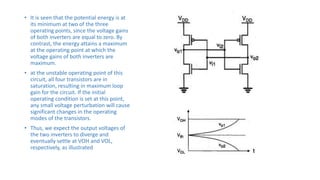
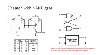
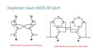
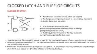
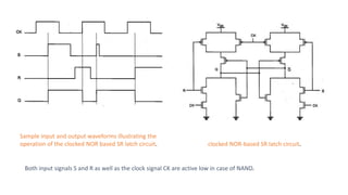
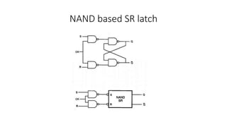
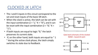
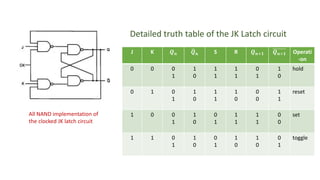
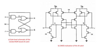
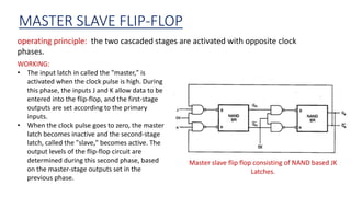
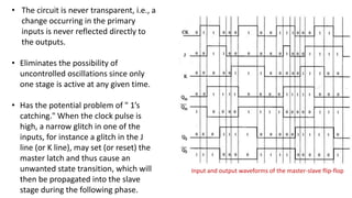
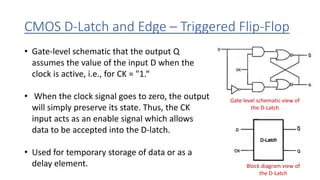


The document provides an in-depth exploration of sequential CMOS logic circuits, focusing on bistable elements, SR latches, and flip-flops. It discusses the operational behavior of these components, including how they respond to inputs during clock cycles and their implications for digital systems. Additionally, it covers the design and function of various configurations such as clocked latches, JK latches, master-slave flip-flops, and D-latches with detailed explanations of their circuit structures and timing characteristics.