Downloaded 849 times
![LAYOUT DESIGN RULES &
GATE LAYOUT
By
S.VARUN
M.Tech [EST]](https://image.slidesharecdn.com/vlsi-160411135631/75/Layout-Stick-Diagram-Design-Rules-1-2048.jpg)
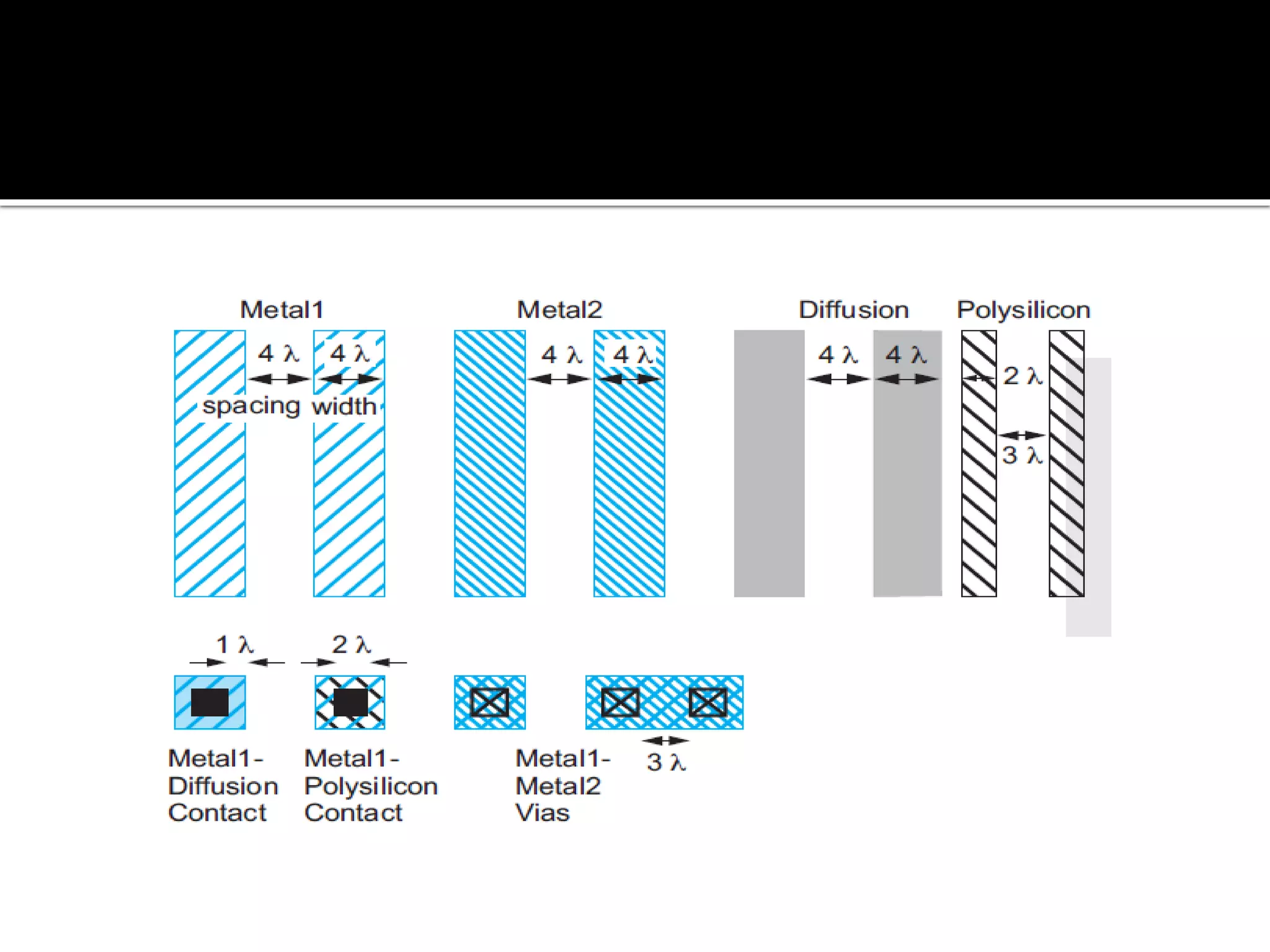
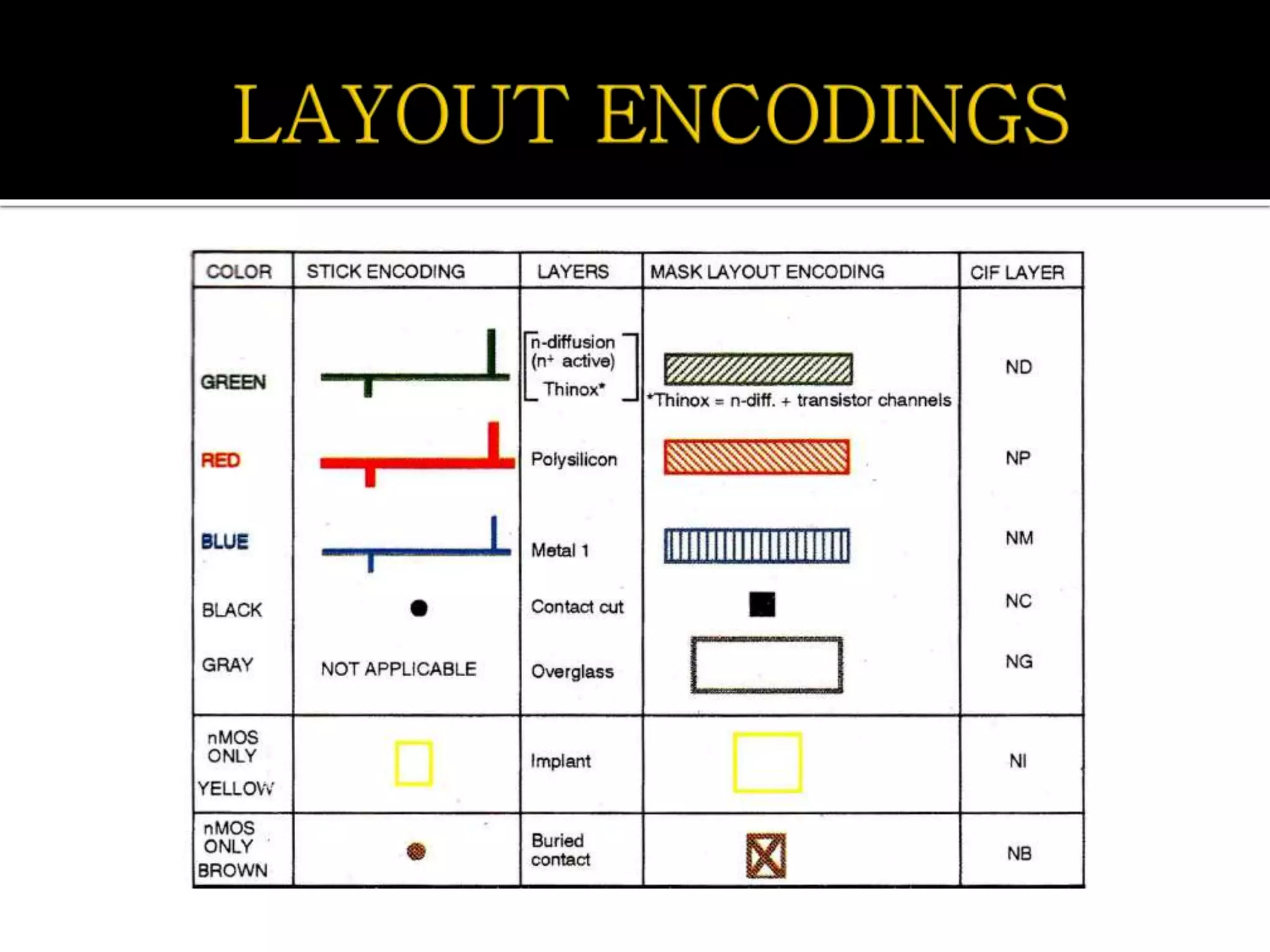
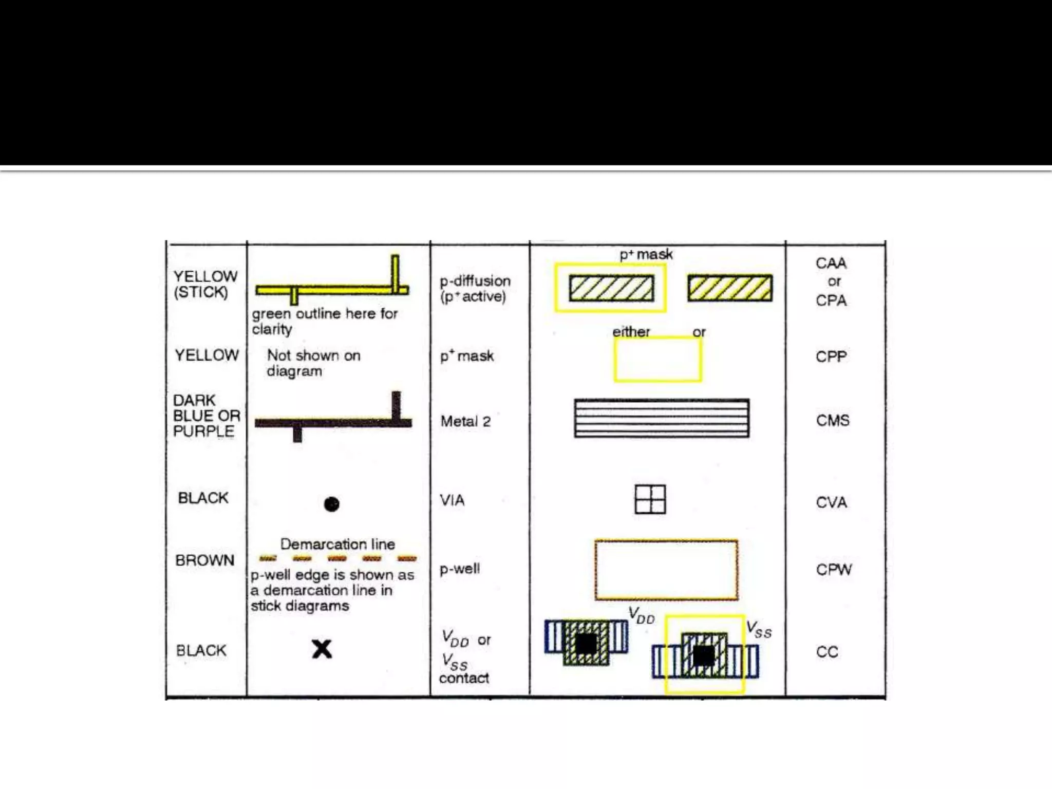
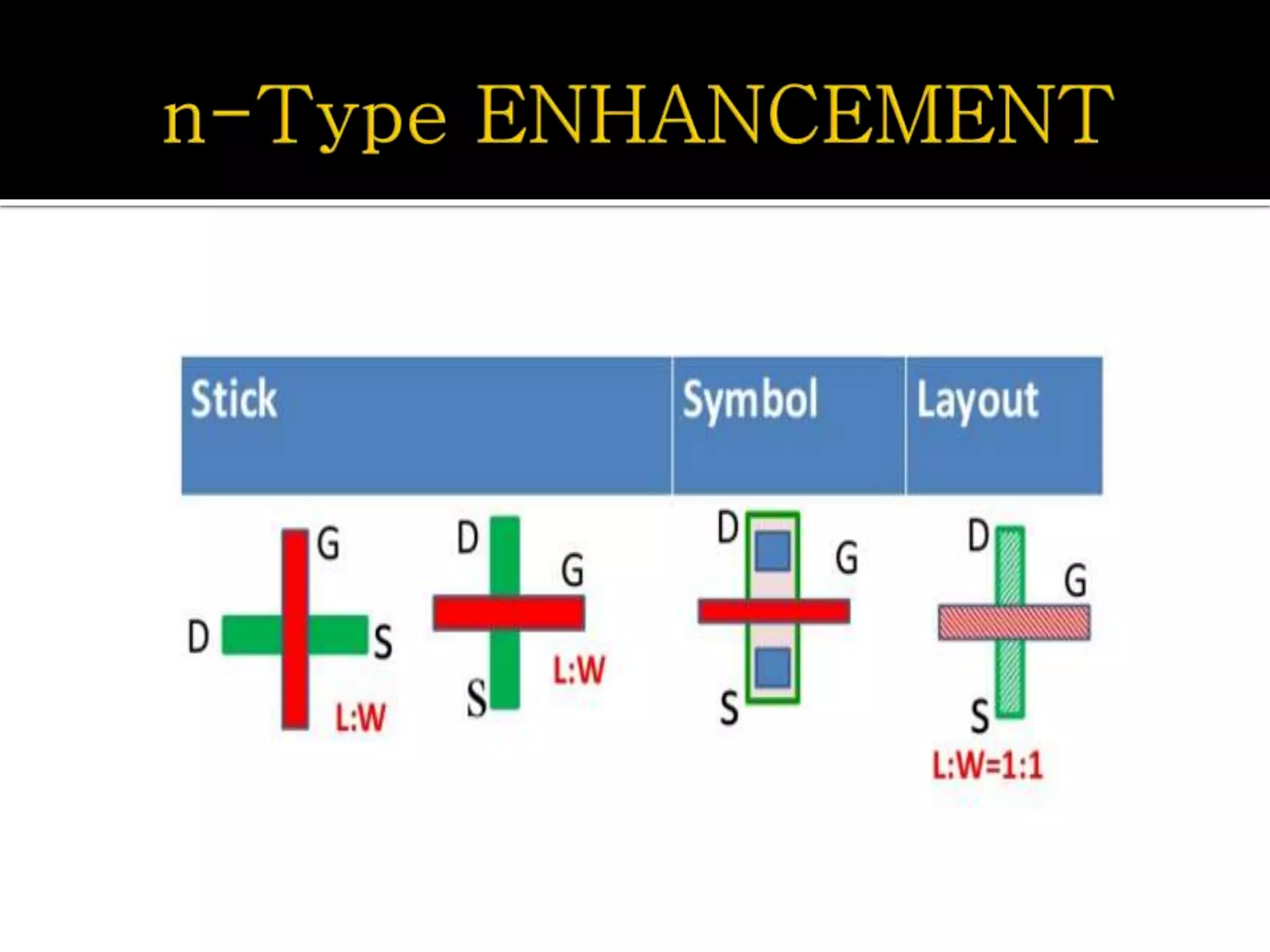
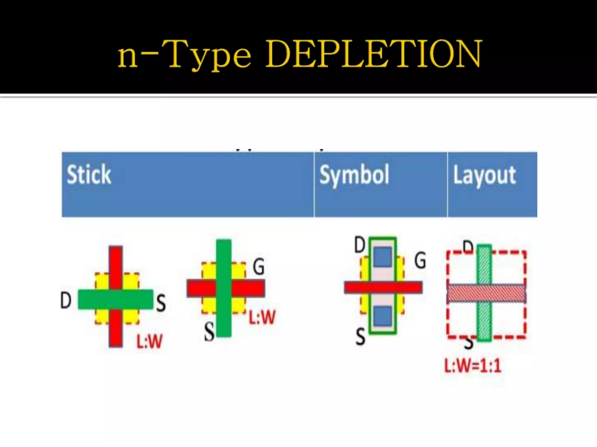
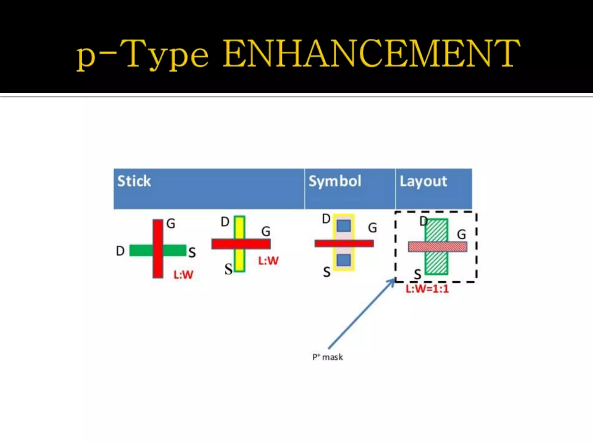
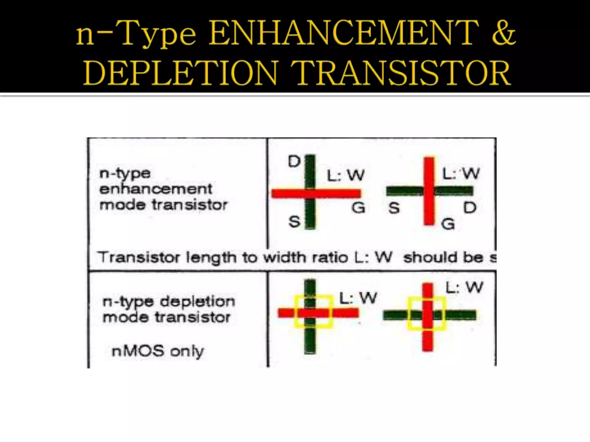
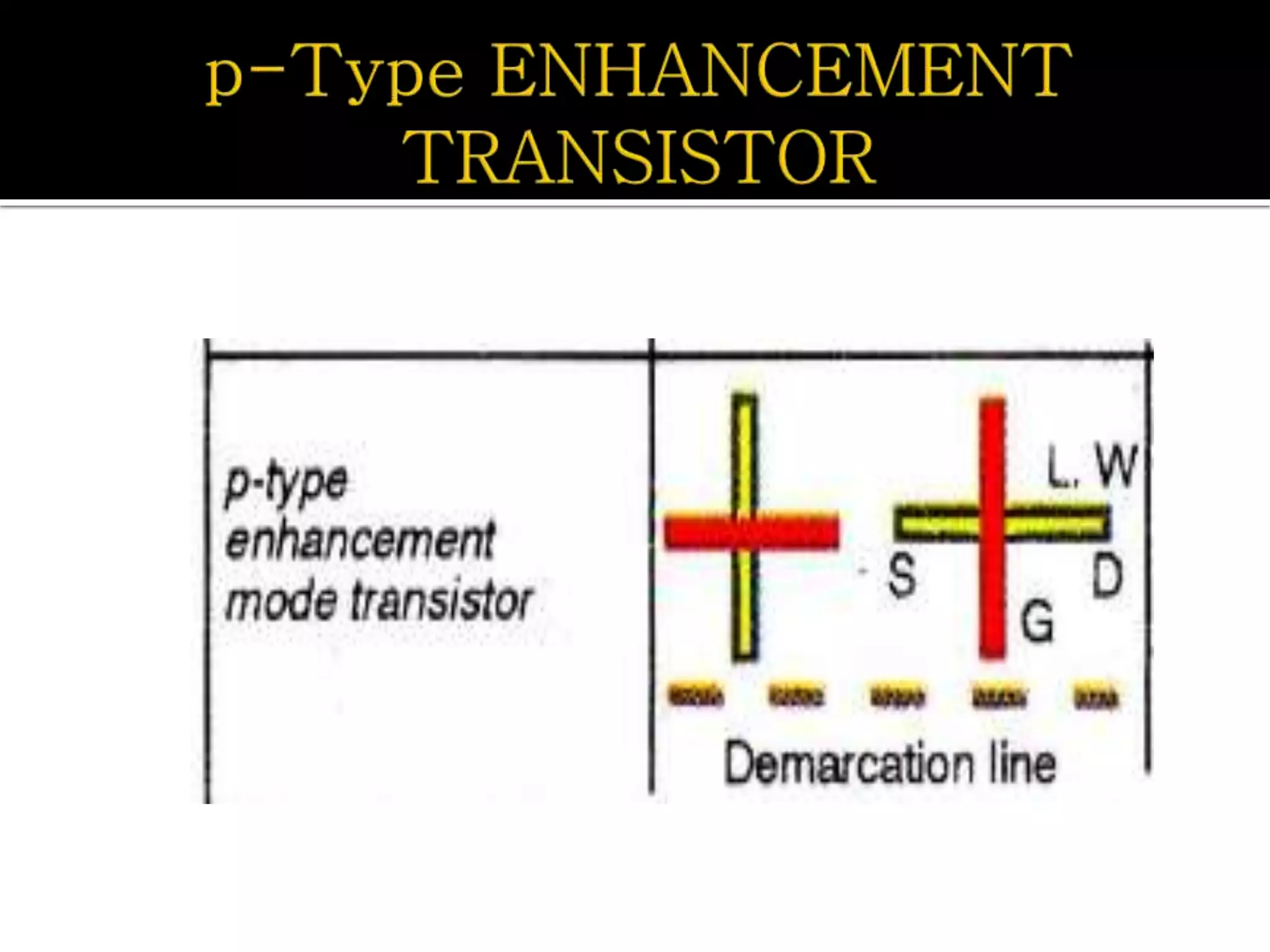
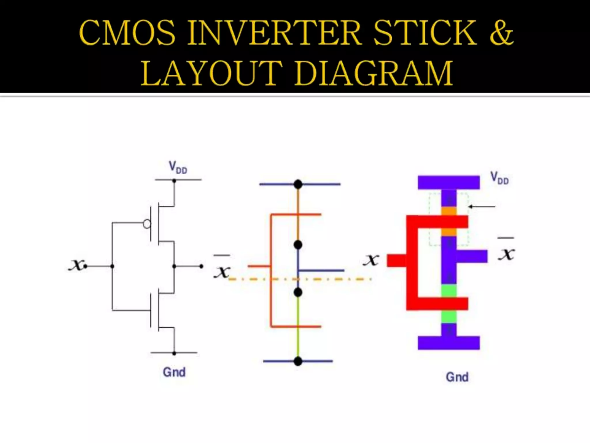
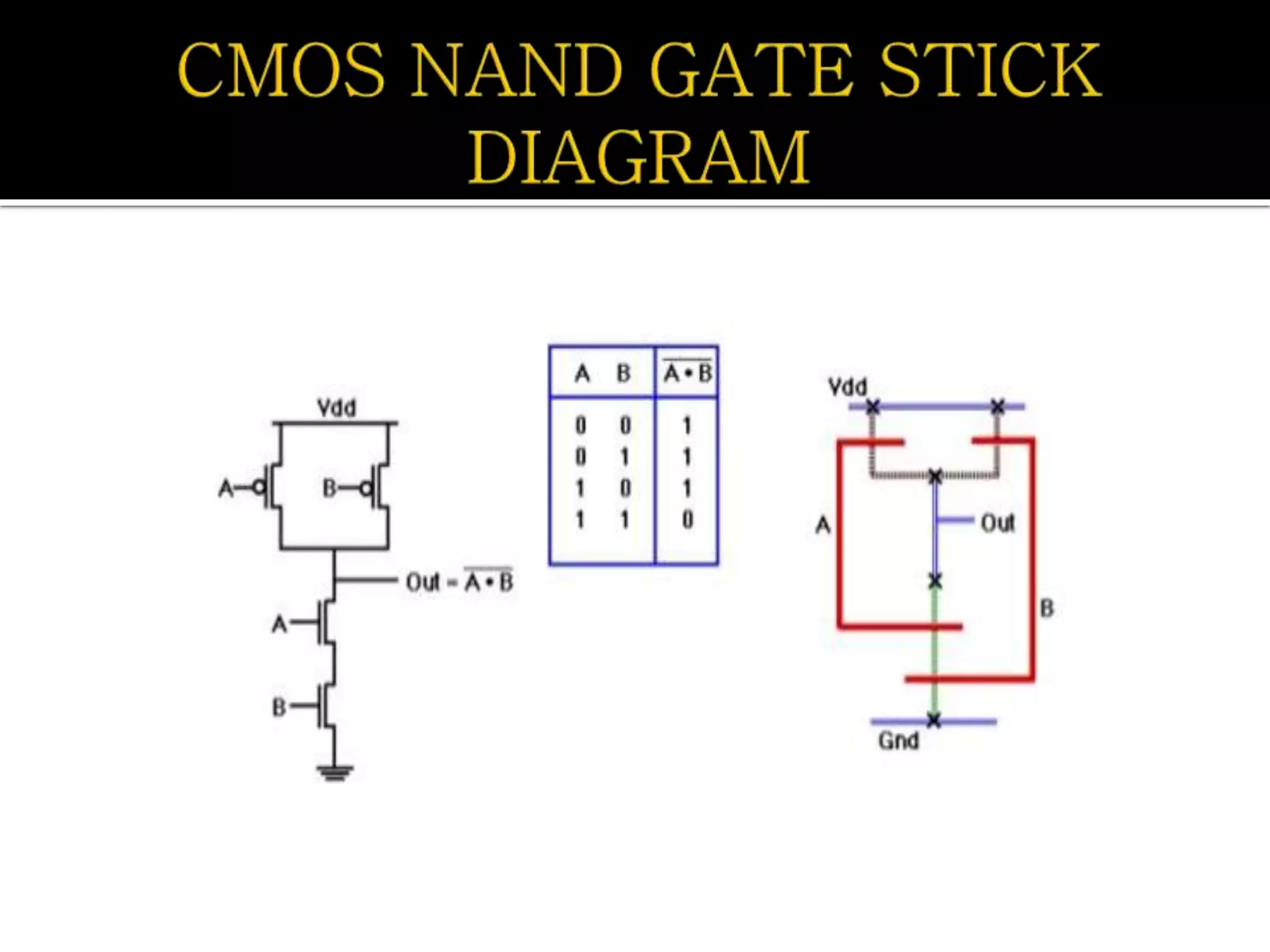
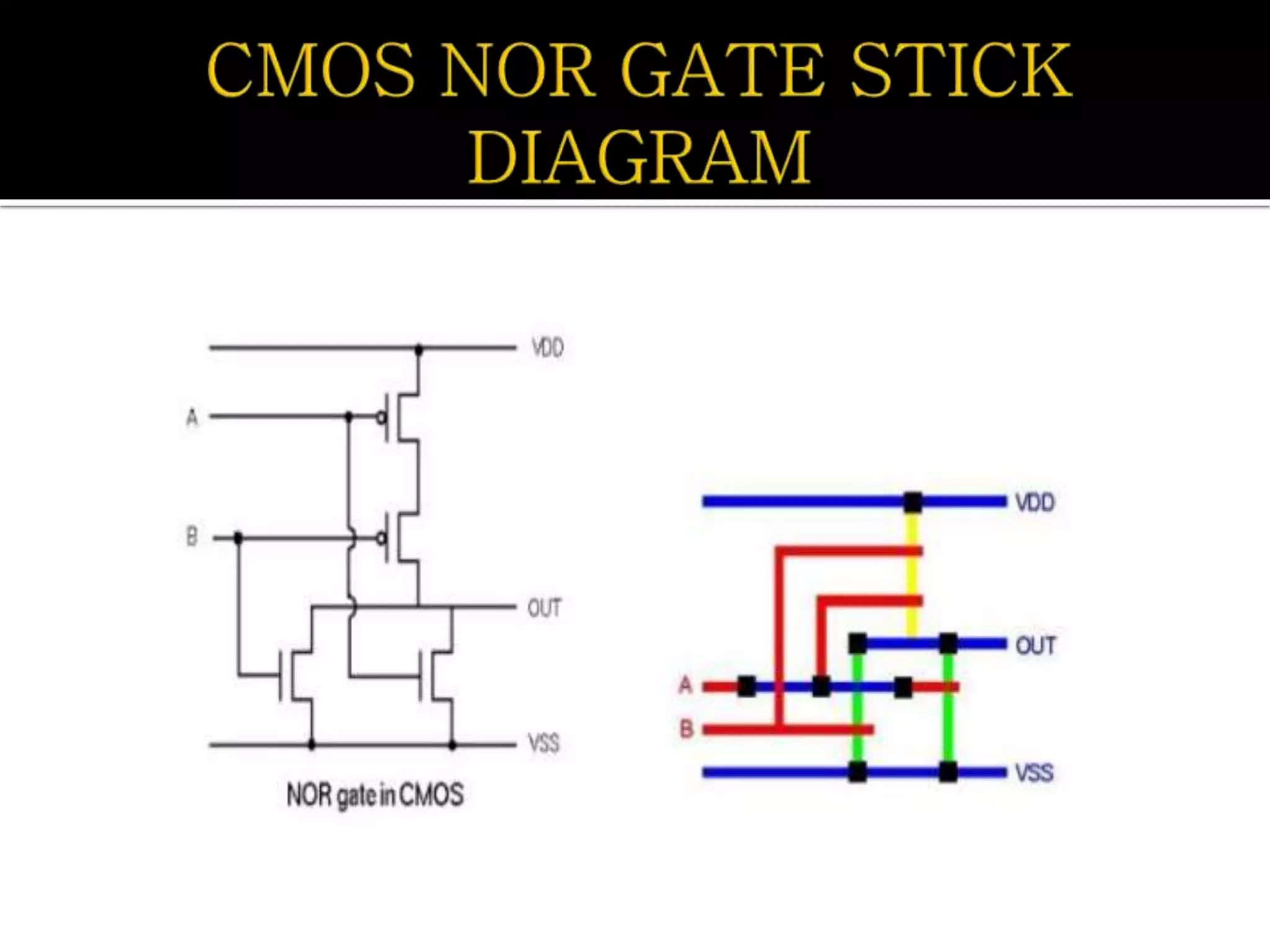
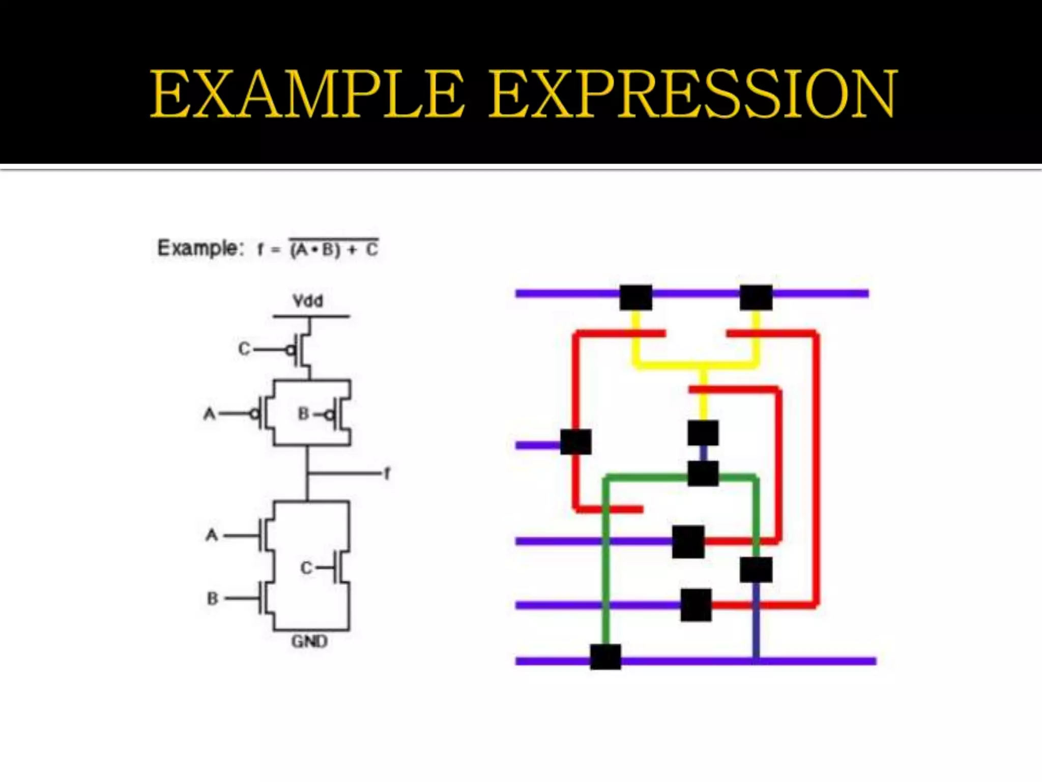


Layout design refers to the arrangement of components in an integrated circuit for fabrication, governed by layout design rules that dictate feature size and packing density. Lambda-based design rules simplify process scaling by using a single parameter to characterize resolution, which is beneficial for uniformity across different manufacturing processes. Stick diagrams visually represent layer information and assist with planning layouts, relative placement of transistors, and signal assignments among other functions.


