Downloaded 3,196 times

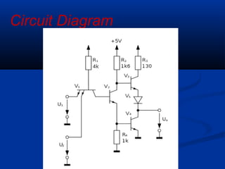
![ So that, Q2 is also turns off.
But at the same time we have L=+VCC, this
voltage is applied on the base of Q4
As a result transistor Q3 is turned ON.
Therefore, the output voltage is given by
V0=+VCC-[Voltage drop in
R4+drop in diode ‘D’]](https://image.slidesharecdn.com/logicfamilies-130116233917-phpapp01/85/Logic-families-25-320.jpg)
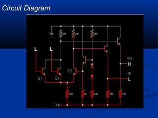


This document discusses different logic families including Resistor Transistor Logic (RTL), Diode Transistor Logic (DTL), Transistor-Transistor Logic (TTL), and Emitter Coupled Logic (ECL). It provides circuit diagrams and explanations of the working principles for each logic family. Key characteristics like fan-in, fan-out, propagation delay, noise immunity, and power dissipation are compared for each logic family.