Downloaded 154 times


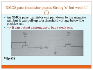


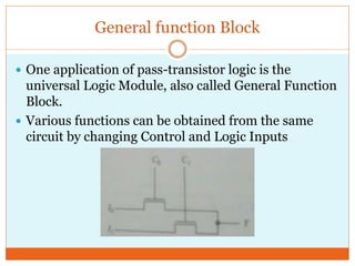
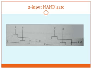
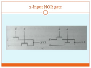
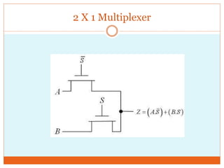
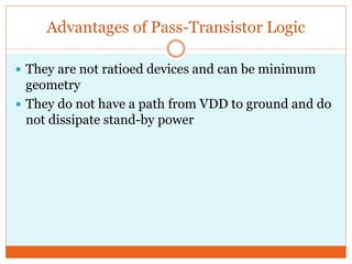
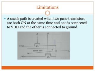
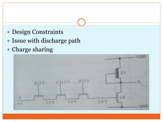
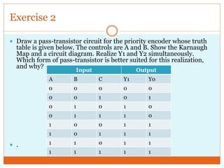

The document discusses pass transistor logic (PTL), explaining how NMOS and PMOS transistors operate to transfer charge between input and output nodes and defines strong and weak logic levels. It describes the limitations and advantages of PTL in circuit design, emphasizing applications like universal logic modules and multiplexers. Additionally, it includes exercises for designing specific pass-transistor circuits like a three-input majority gate and a priority encoder, illustrating the practical application of the concepts discussed.