Downloaded 243 times


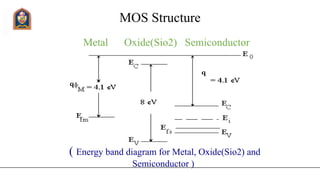
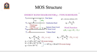
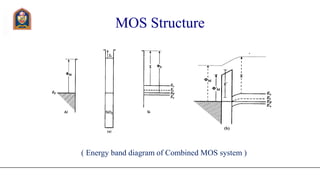
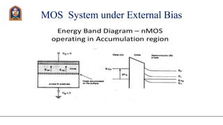
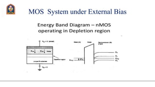
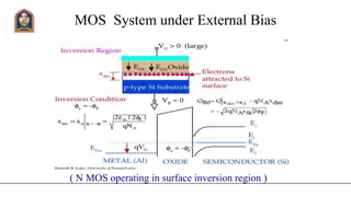
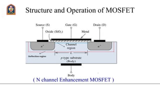
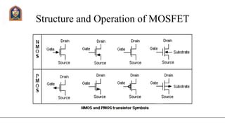
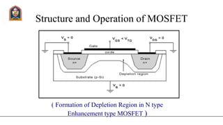
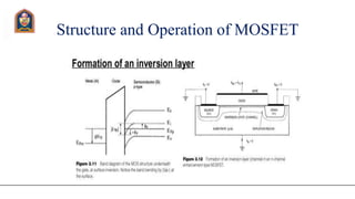
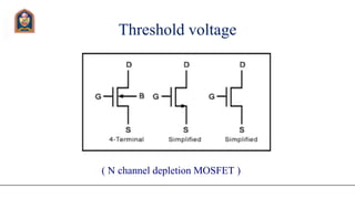
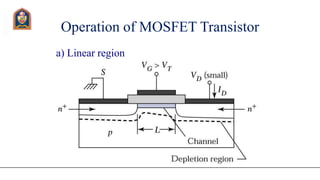
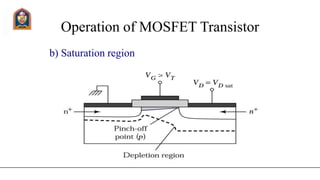
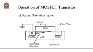
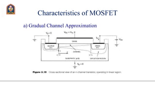
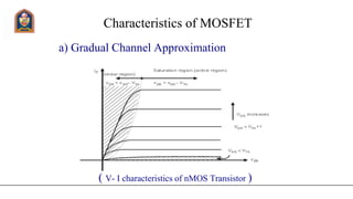
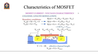
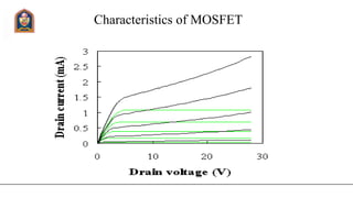
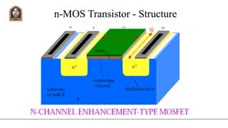
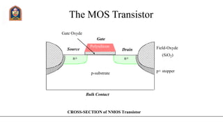
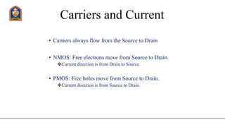
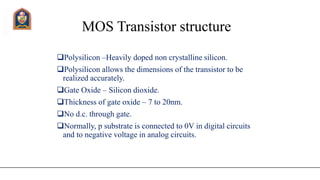
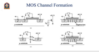
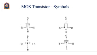


The document discusses the structure and operation of MOS transistors. It describes the basic MOS structure which consists of a metal gate separated from a semiconductor substrate by an oxide layer. Applying a voltage to the gate can induce an inversion layer in the semiconductor to form a channel between the source and drain, allowing current to flow. The threshold voltage is the minimum gate voltage required to form an inversion layer. The document discusses n-channel MOSFETs and their characteristics in different regions of operation defined by the gate-source voltage.


