Downloaded 357 times


The document provides a comprehensive overview of CMOS technology, including the construction and operation of n-type (NMOS) and p-type (PMOS) transistors, which are essential components in creating metal-oxide-semiconductor structures. It explains the principles of transistor operation, how they function as switches, and discusses logic gates such as CMOS inverters and NAND/NOR gates, highlighting their configurations and behaviors. Additionally, it introduces the concepts of pass transistors and transmission gates, addressing their strengths and weaknesses in signal transmission.
An introduction to CMOS Logic, presented by Sudhanshu Janwadkar, detailing the lecture dates.
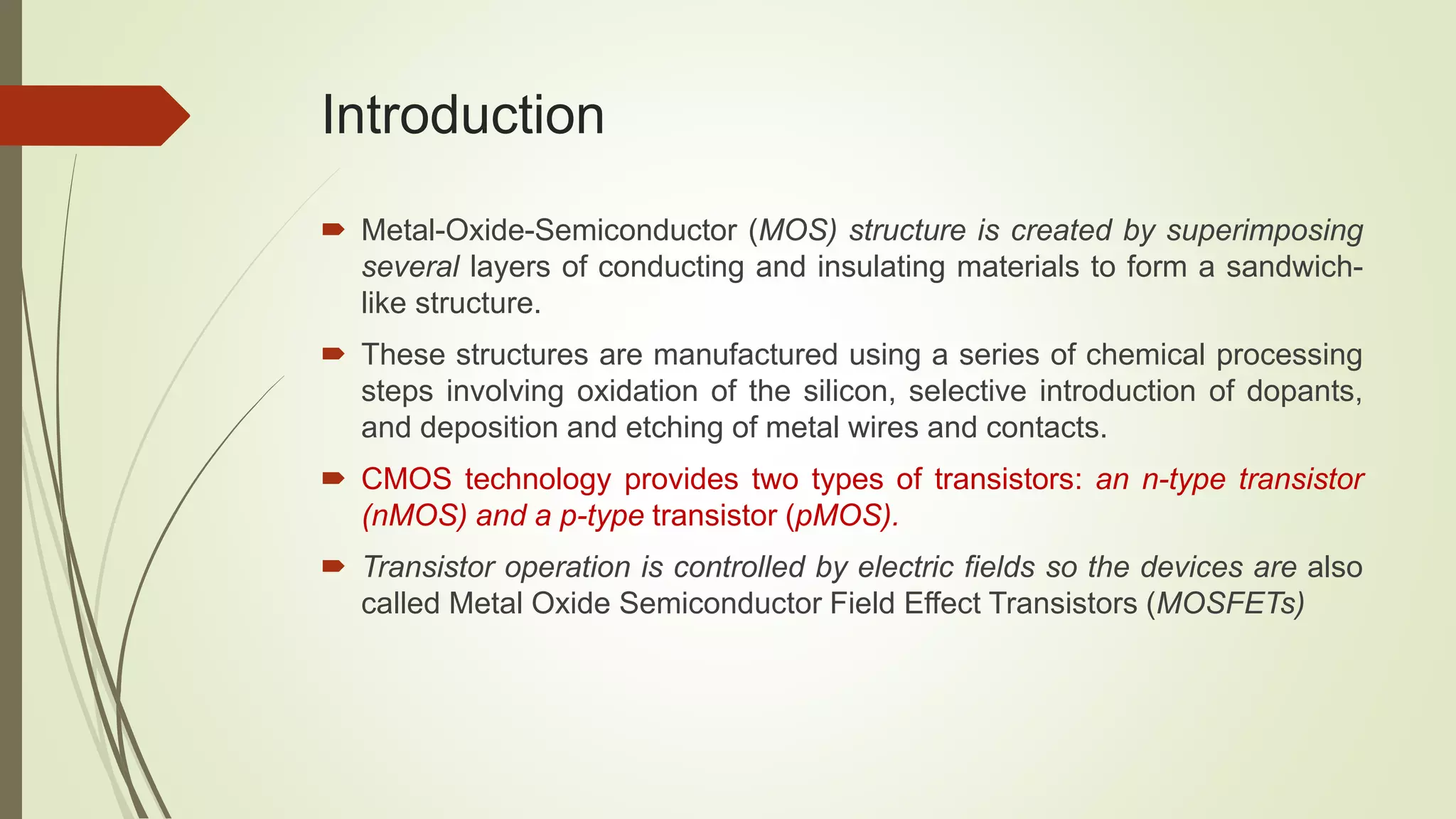
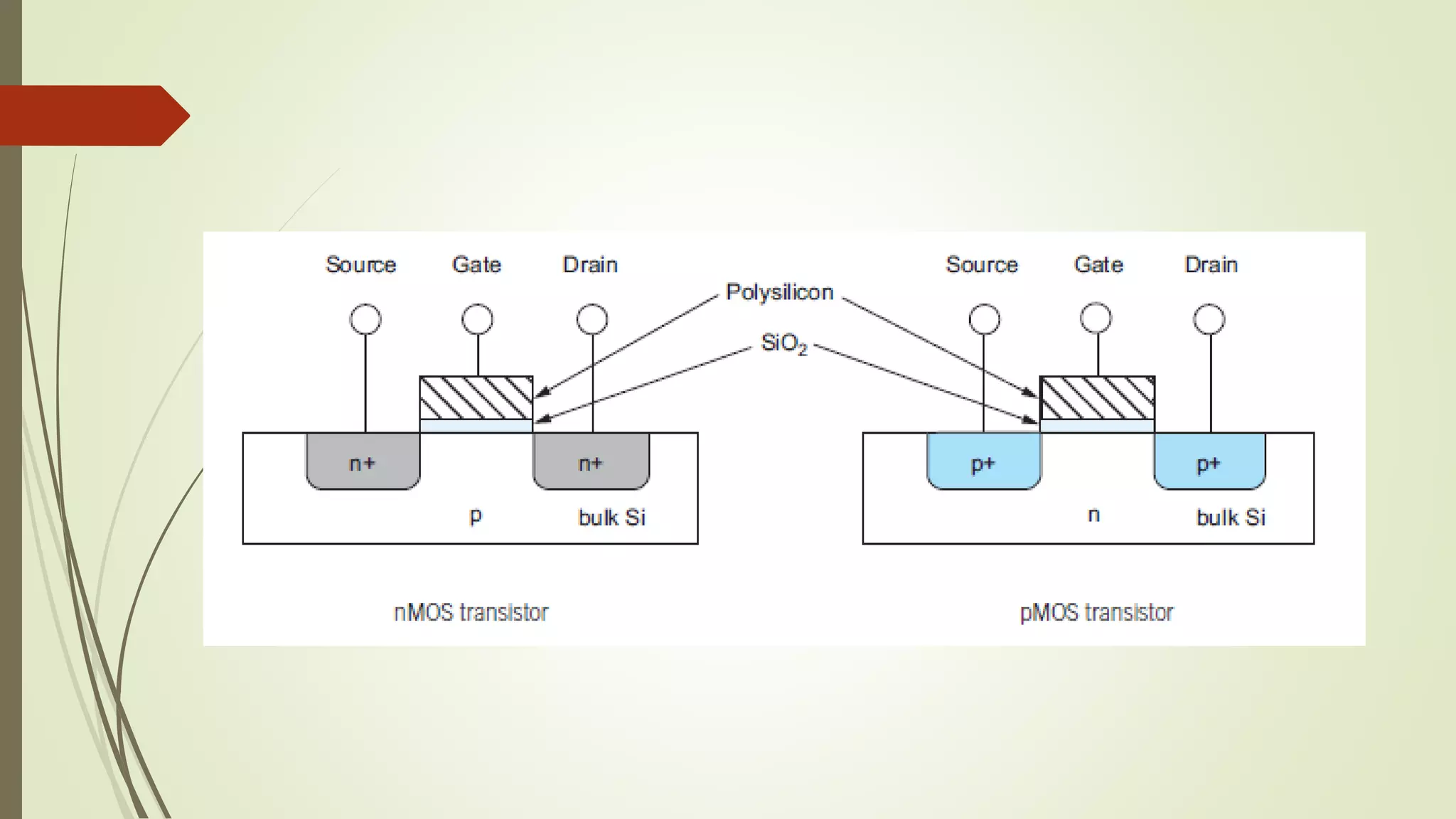
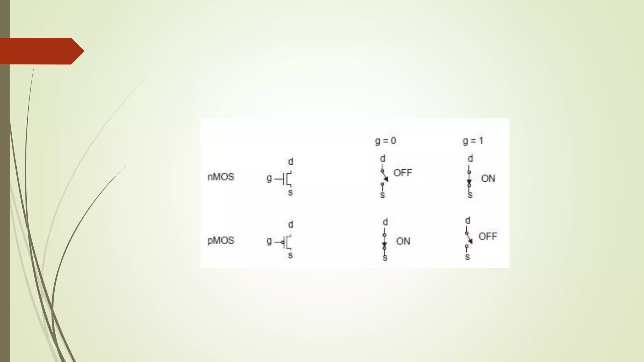
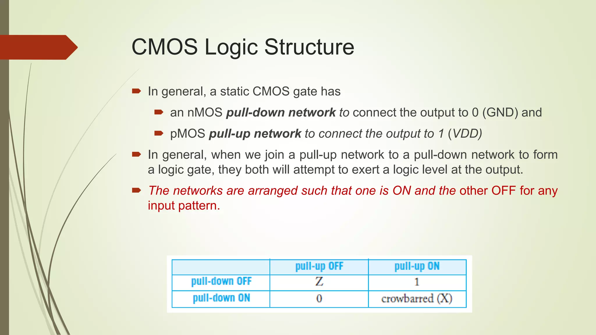
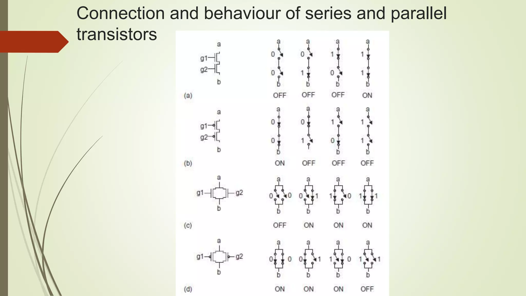
Overview of CMOS technology, its structure, and the functioning of nMOS and pMOS transistors as switches.
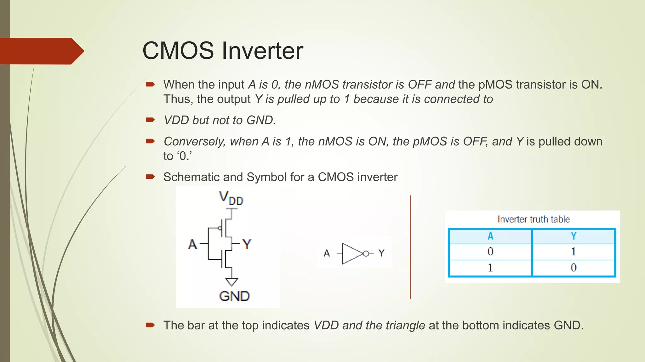
Functionality of a CMOS inverter, explaining how input levels affect output states between VDD and GND.
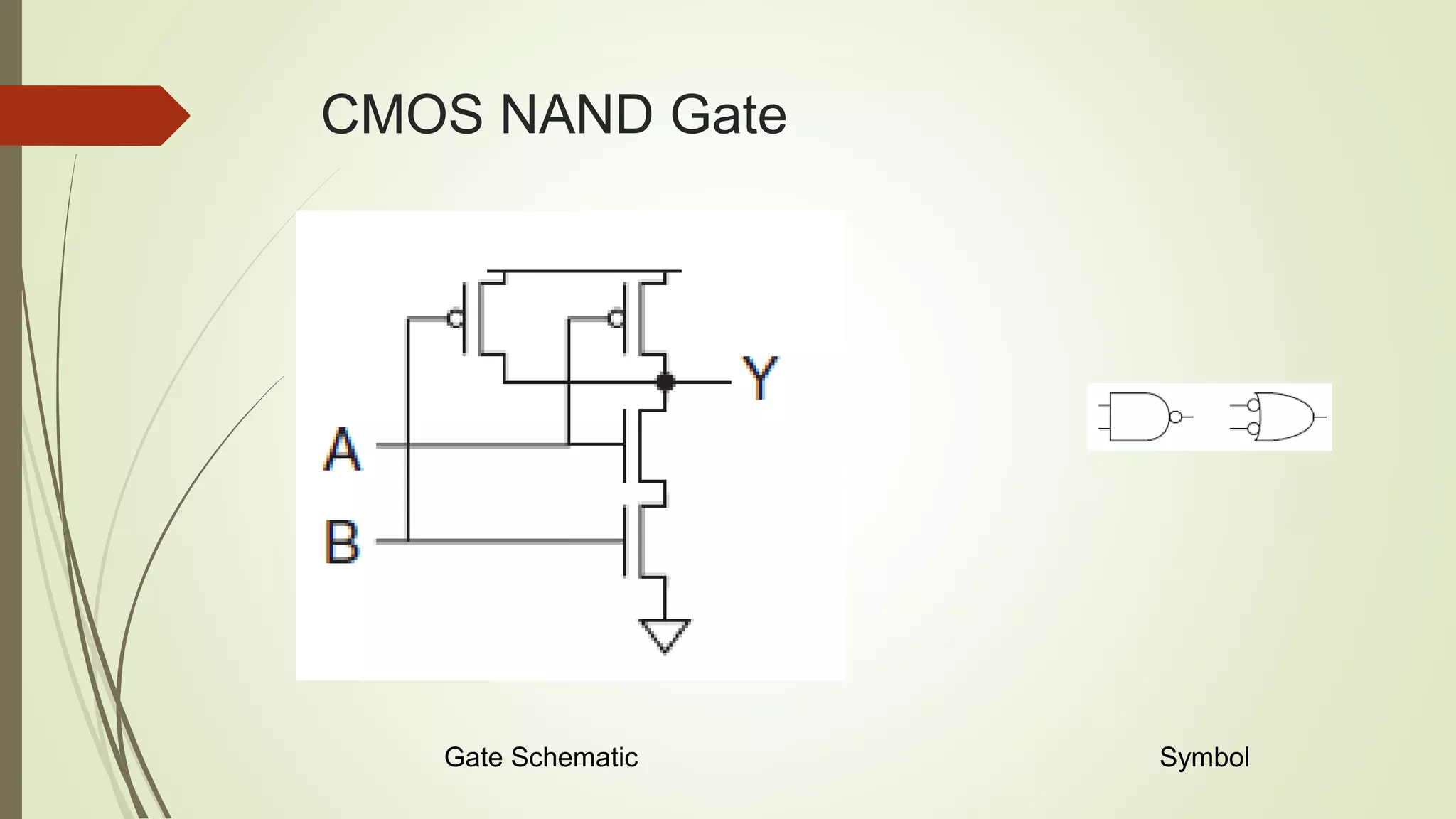
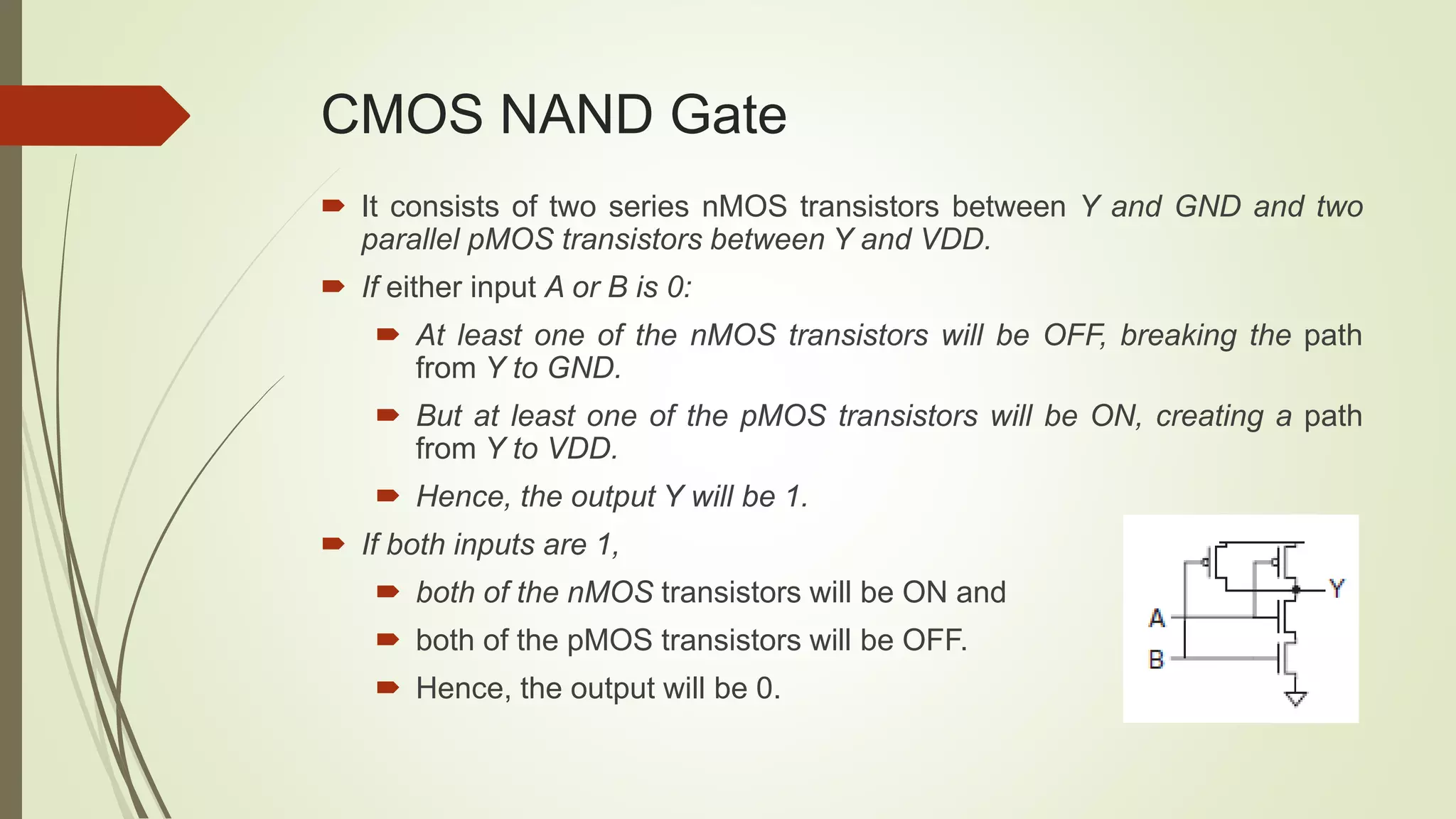
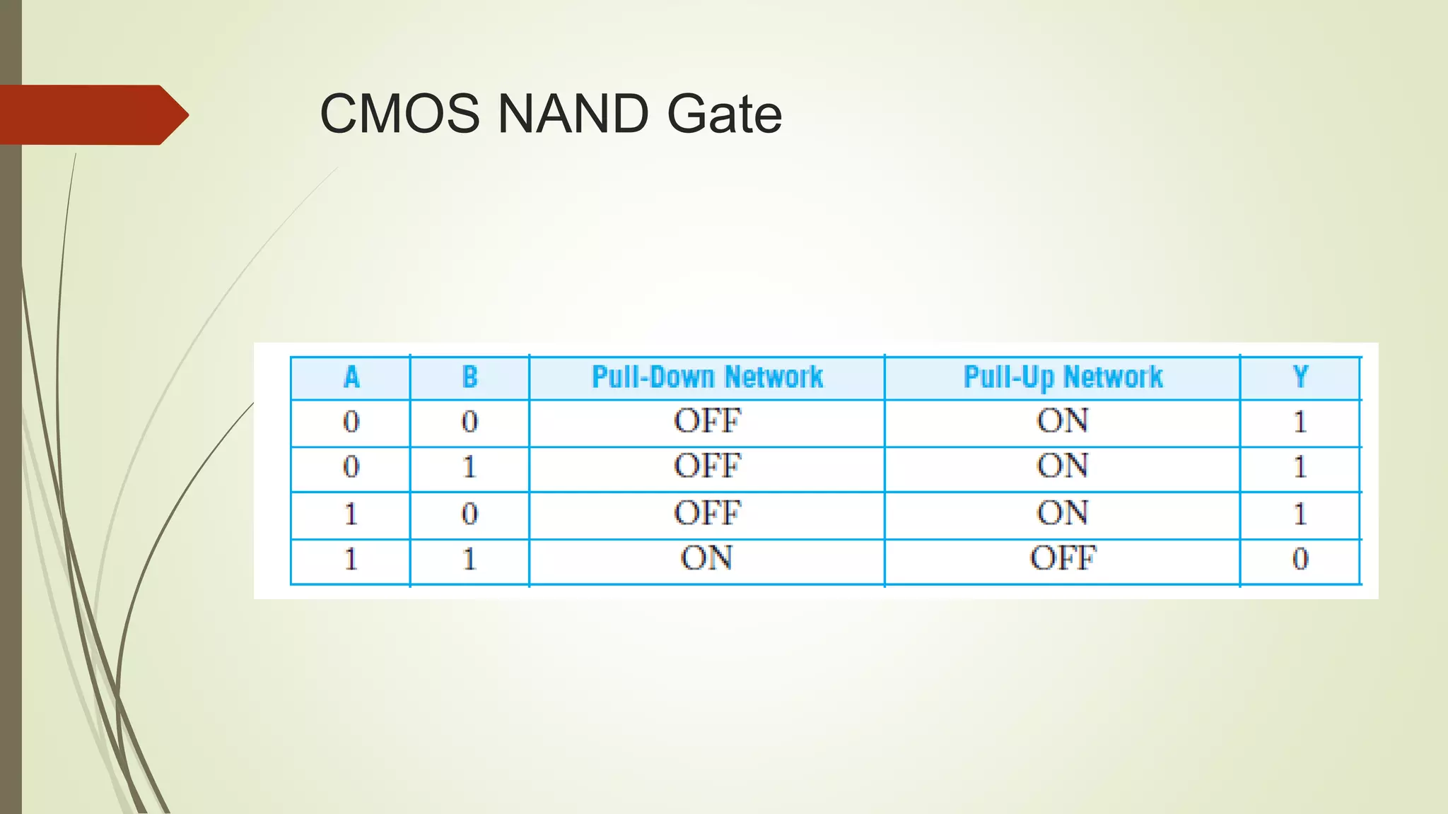
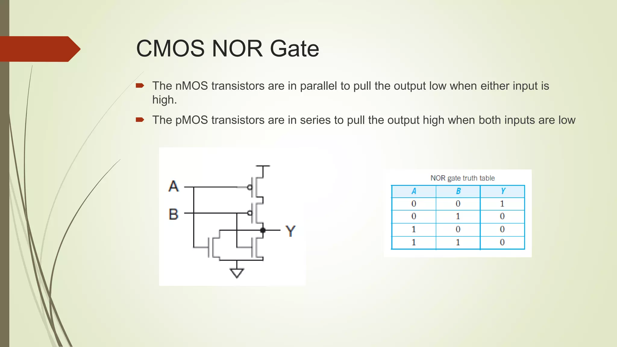
Structure and function of CMOS NAND and NOR Gates, including operations of inputs and outputs.
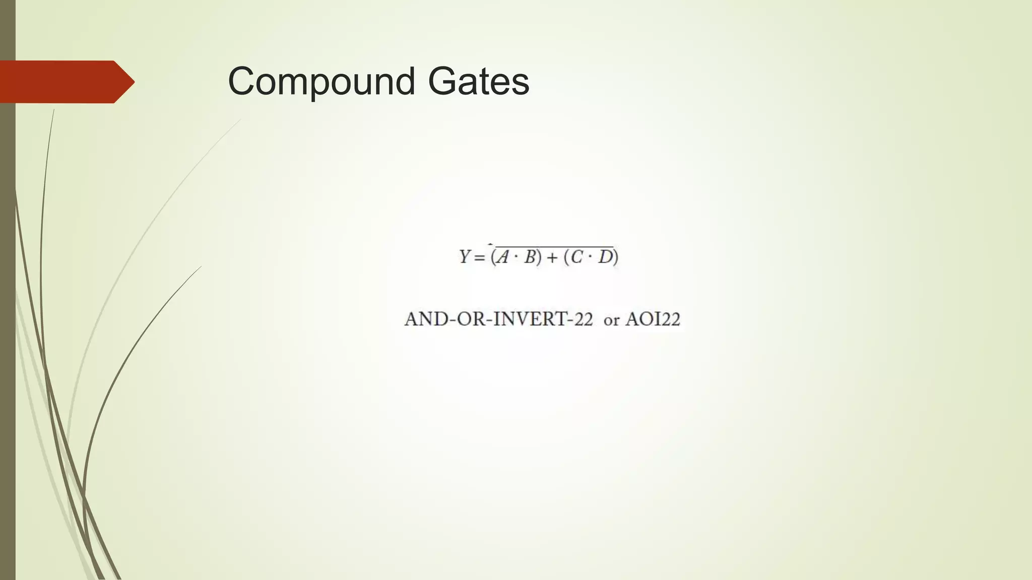
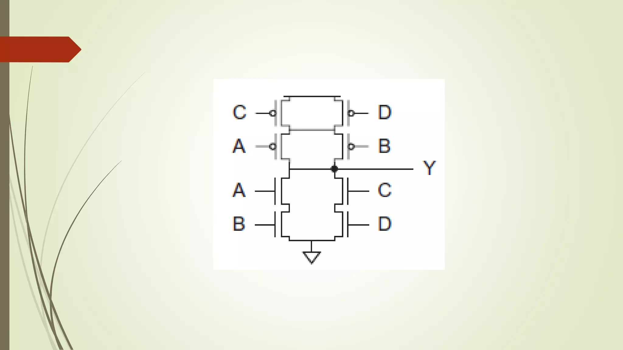
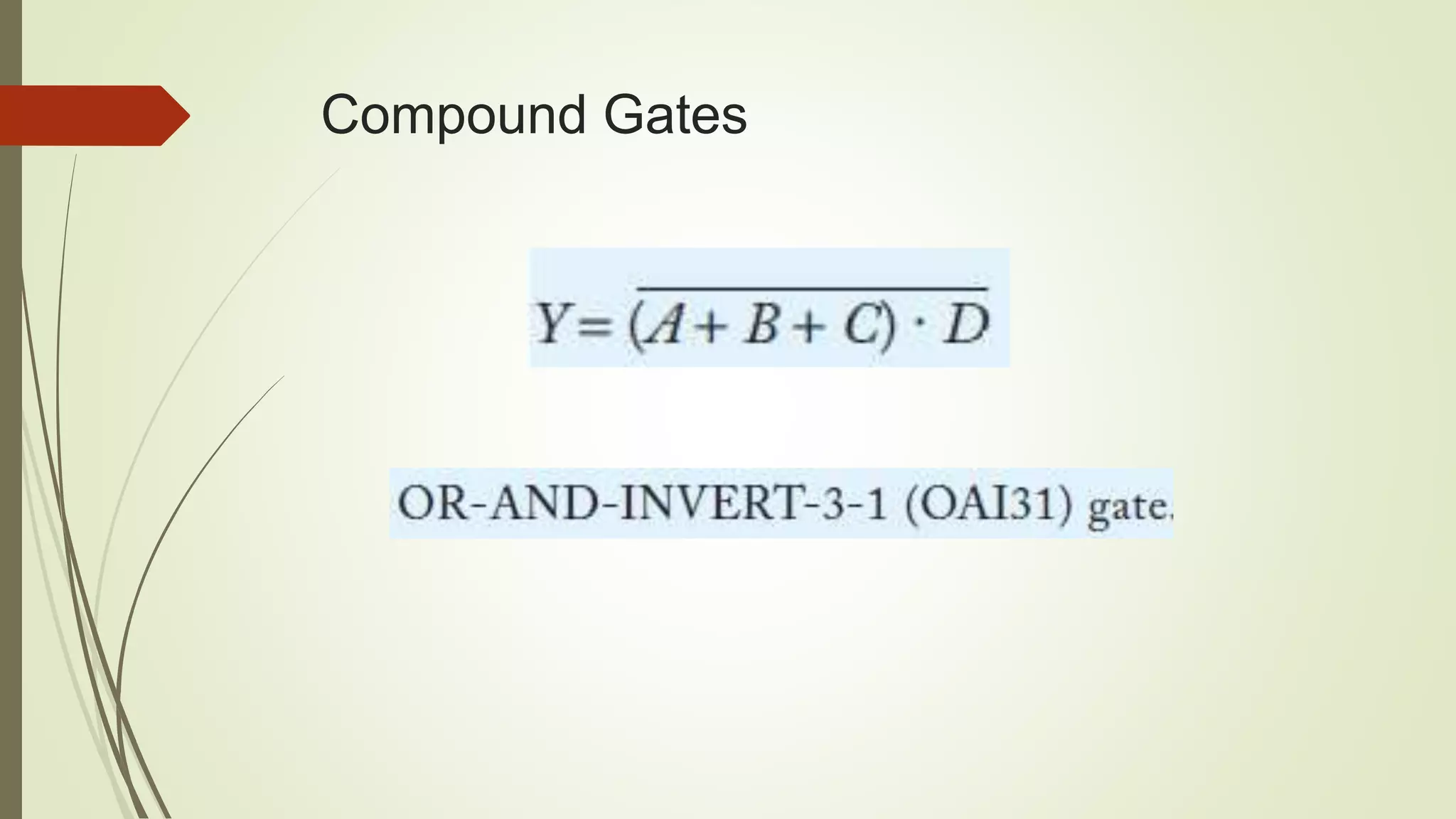
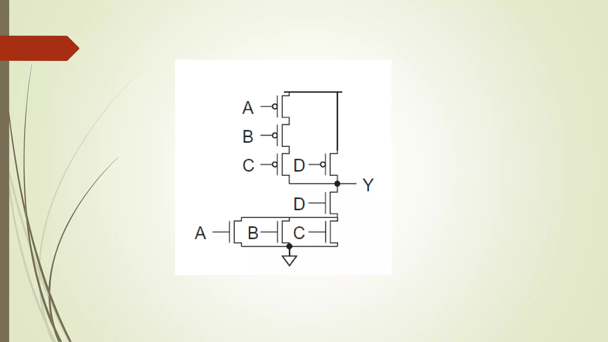
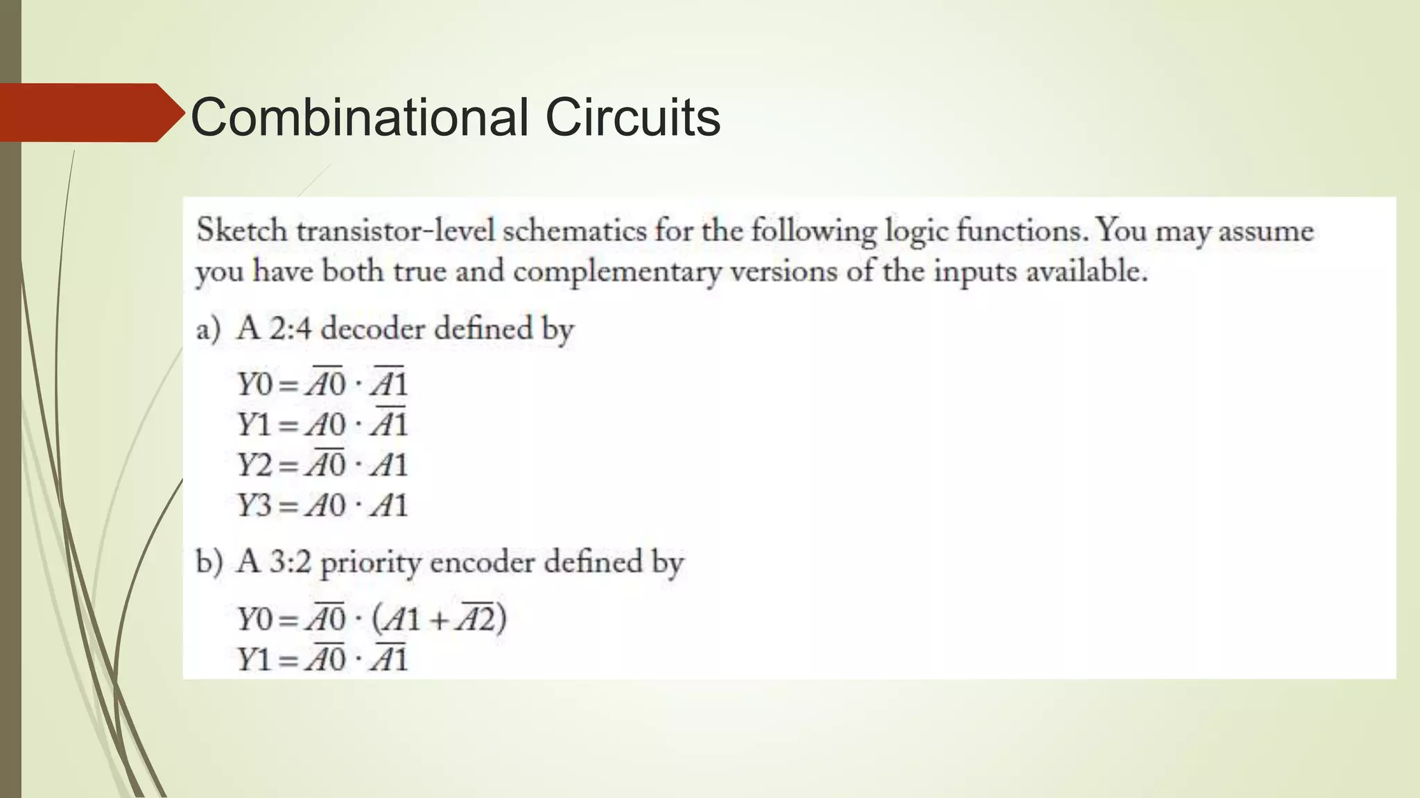
Introduction to compound gates and their setup in the context of combinational circuits.
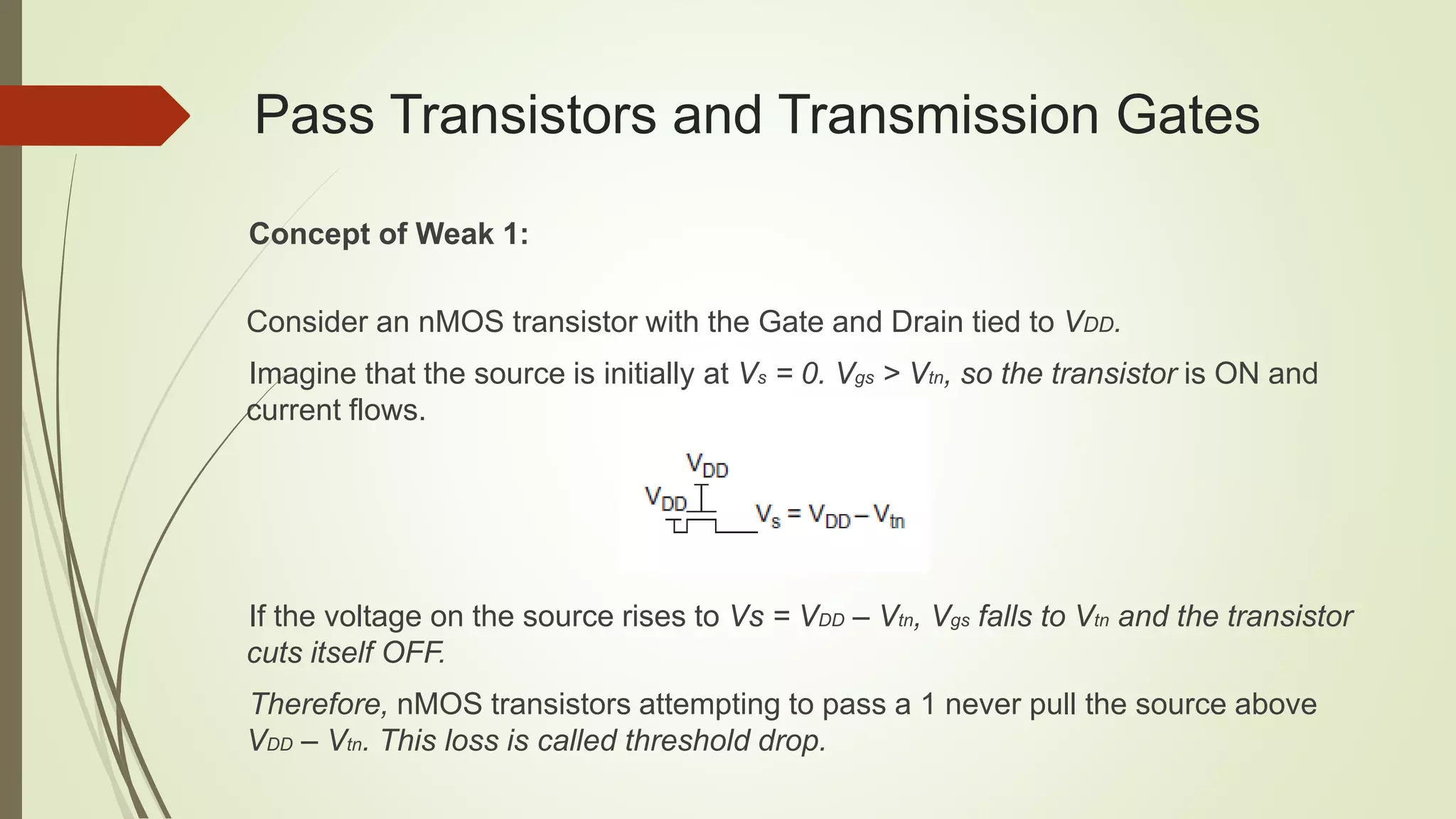
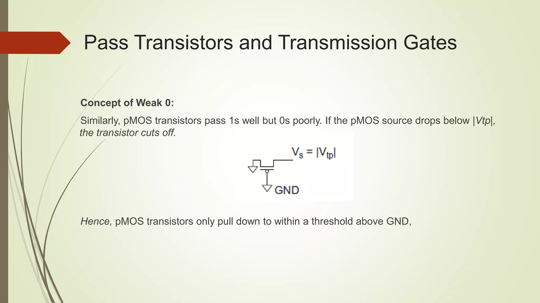
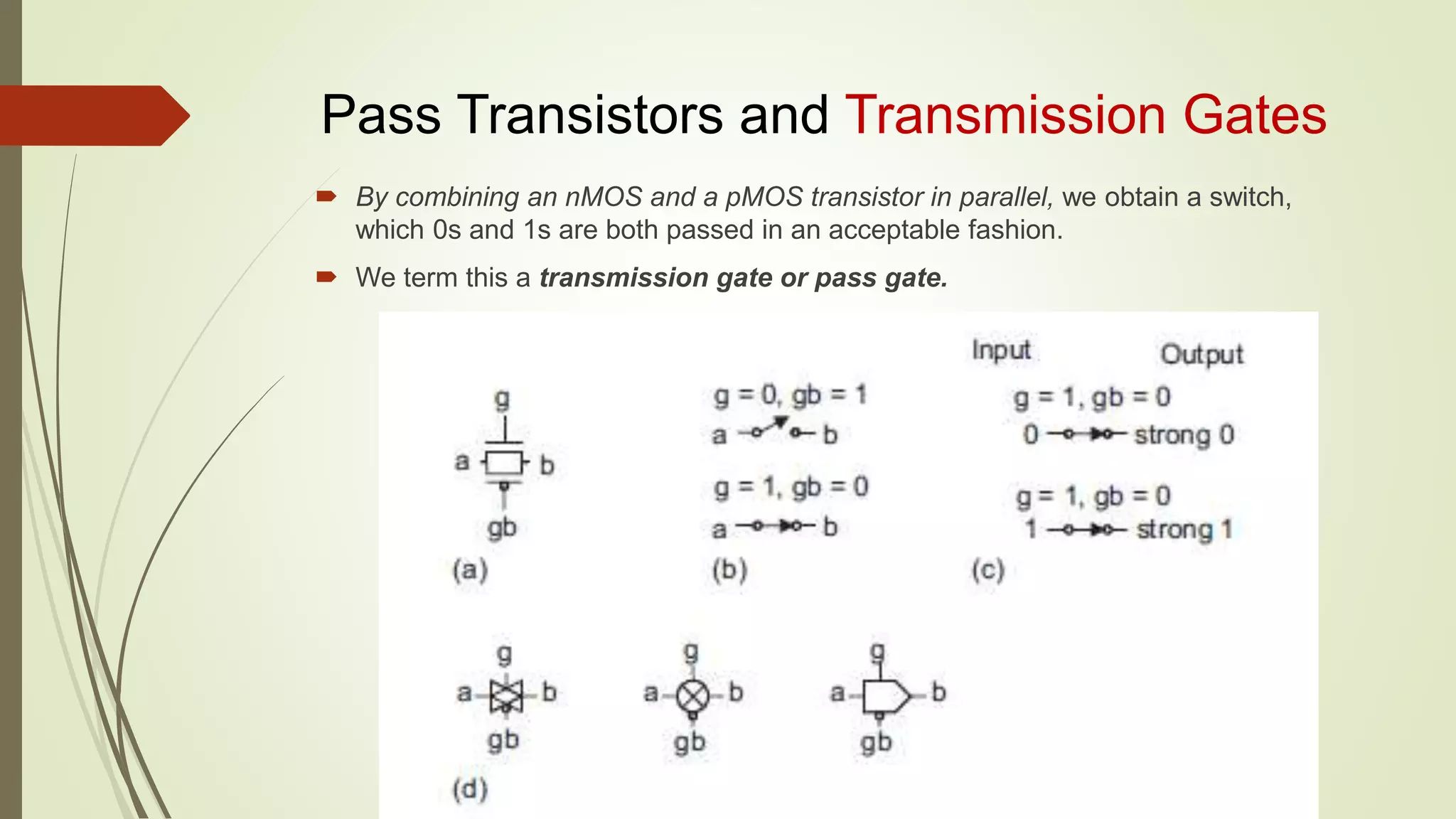
Exploration of pass transistors and transmission gates, highlighting how they manage signal strength.