Download as PDF, PPTX
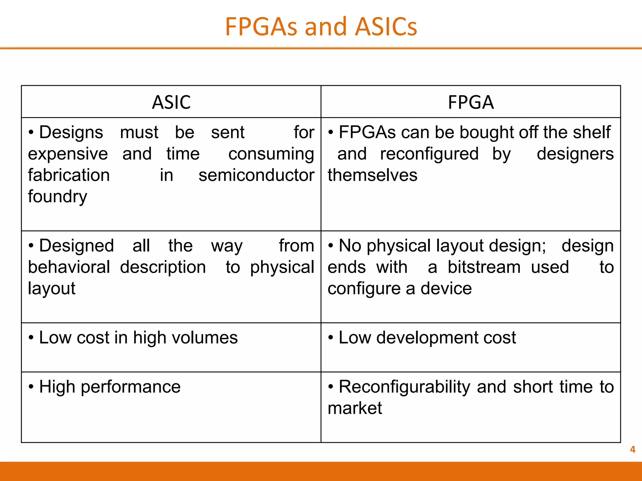
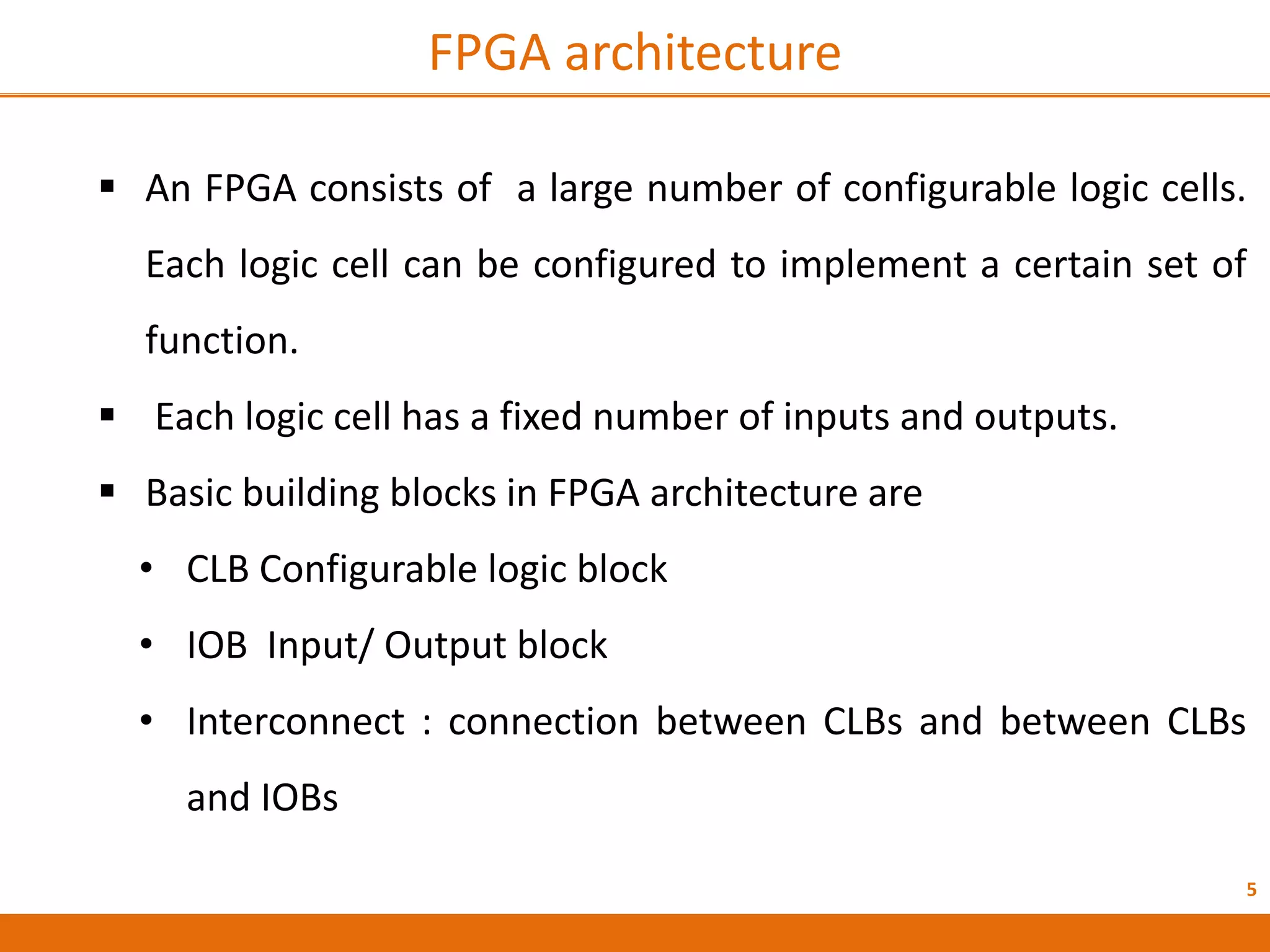
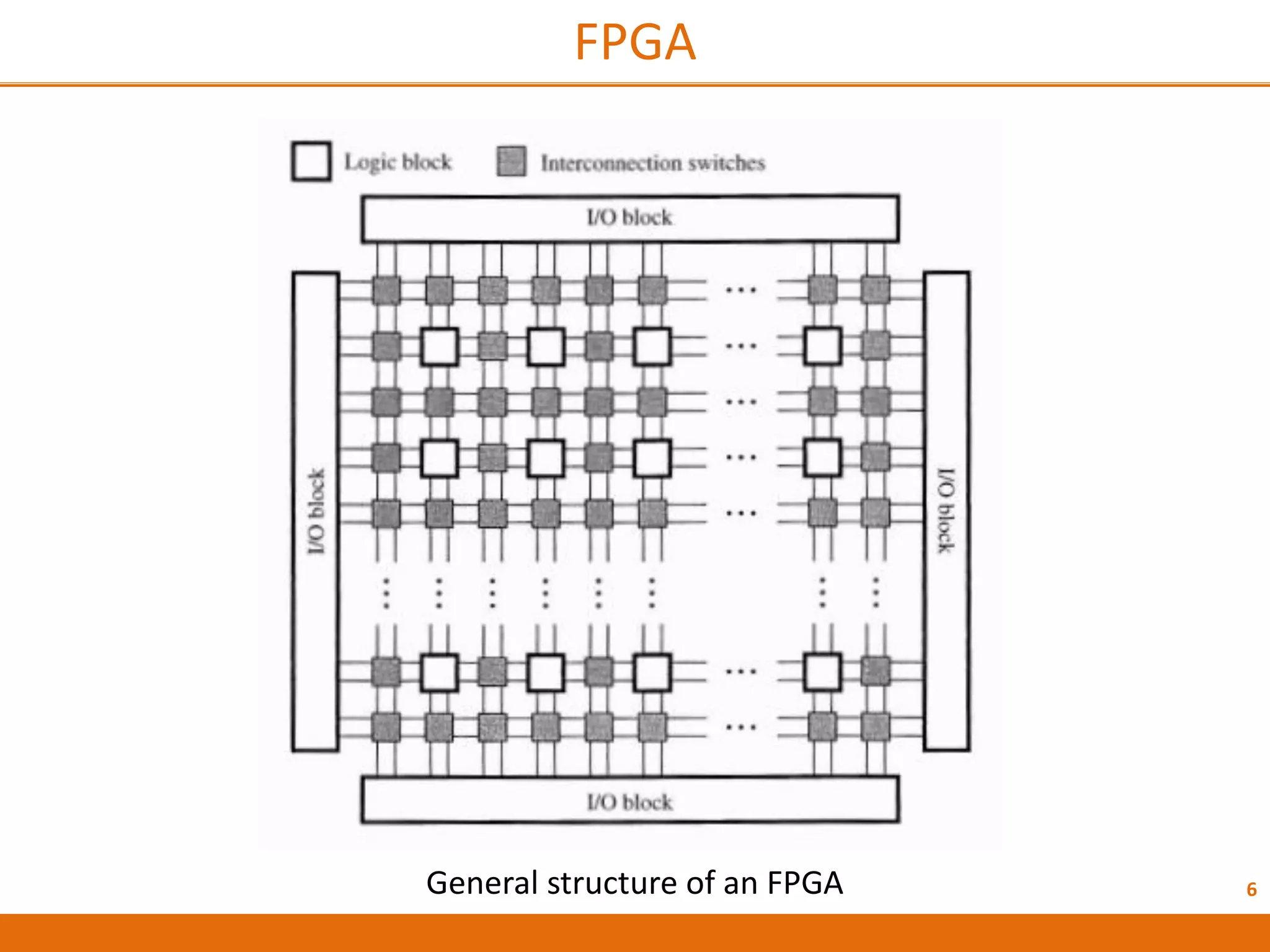
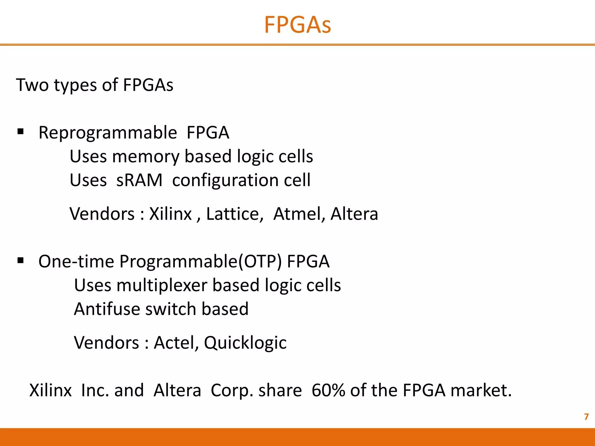
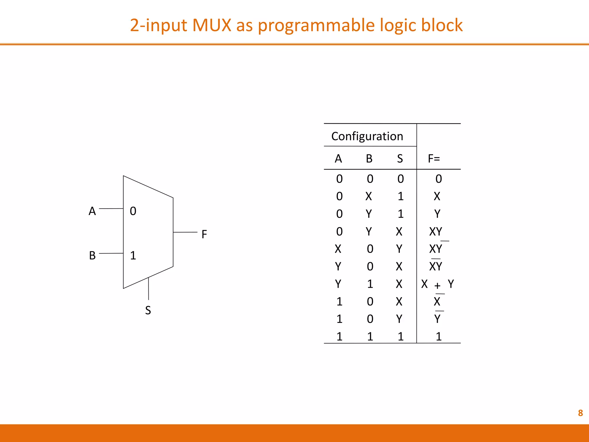
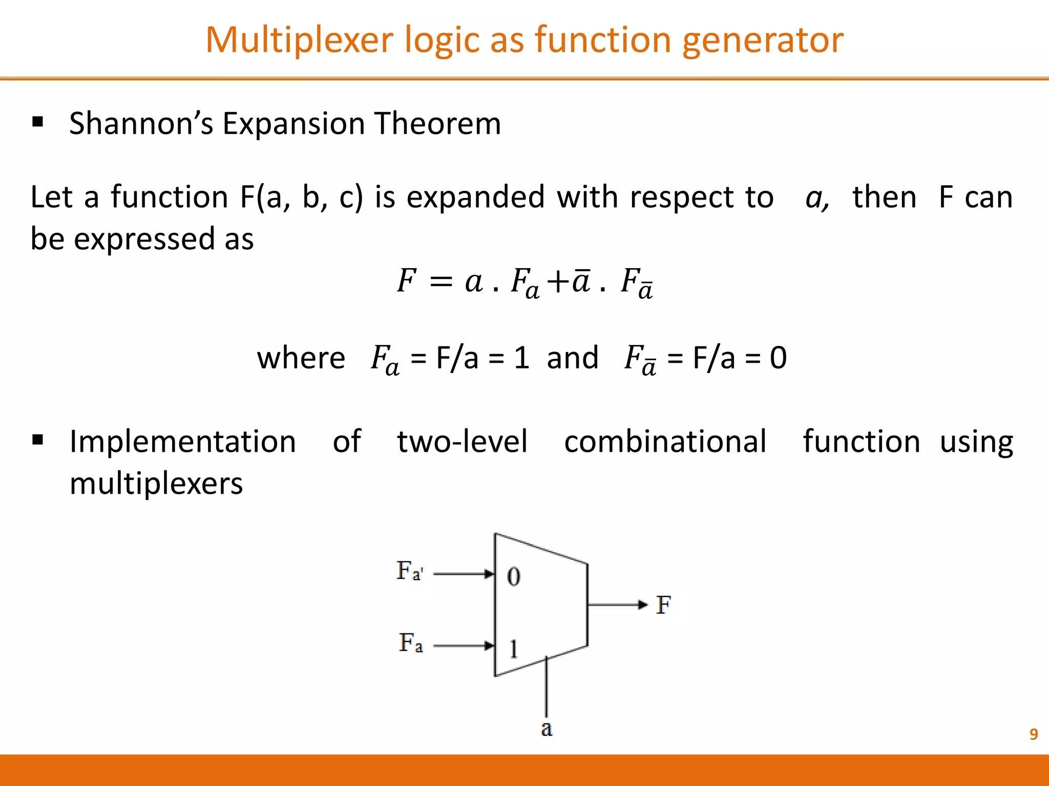
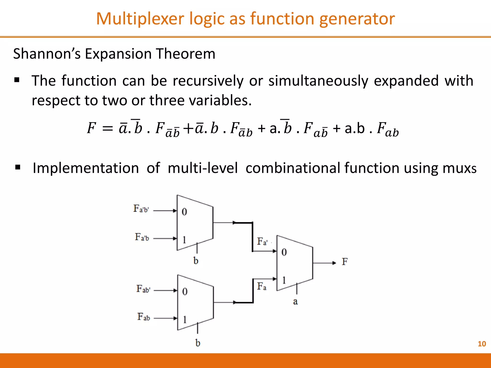
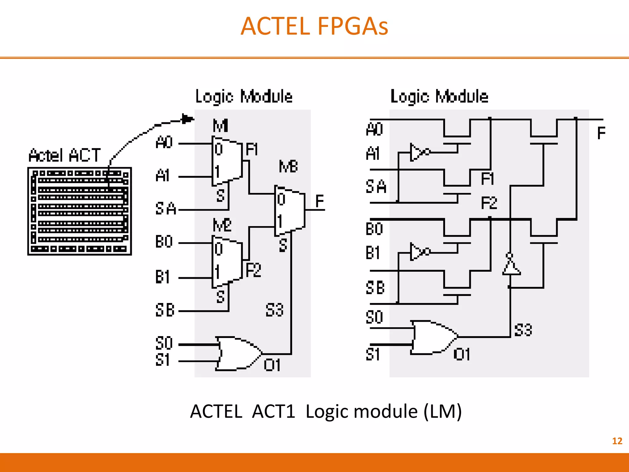
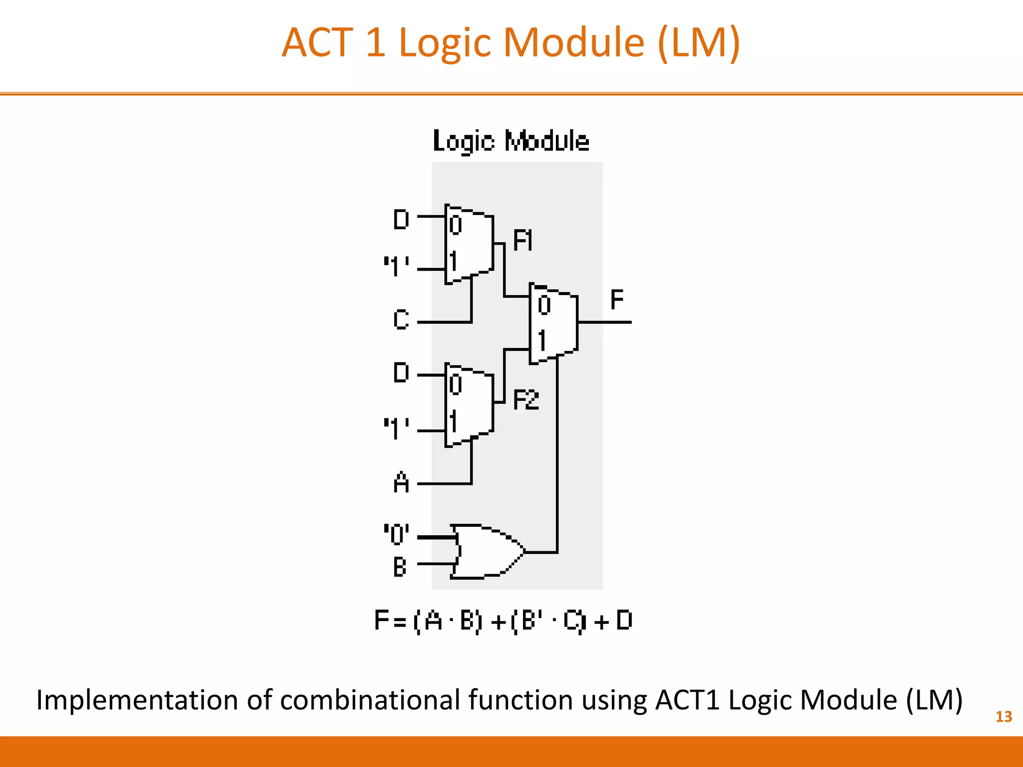
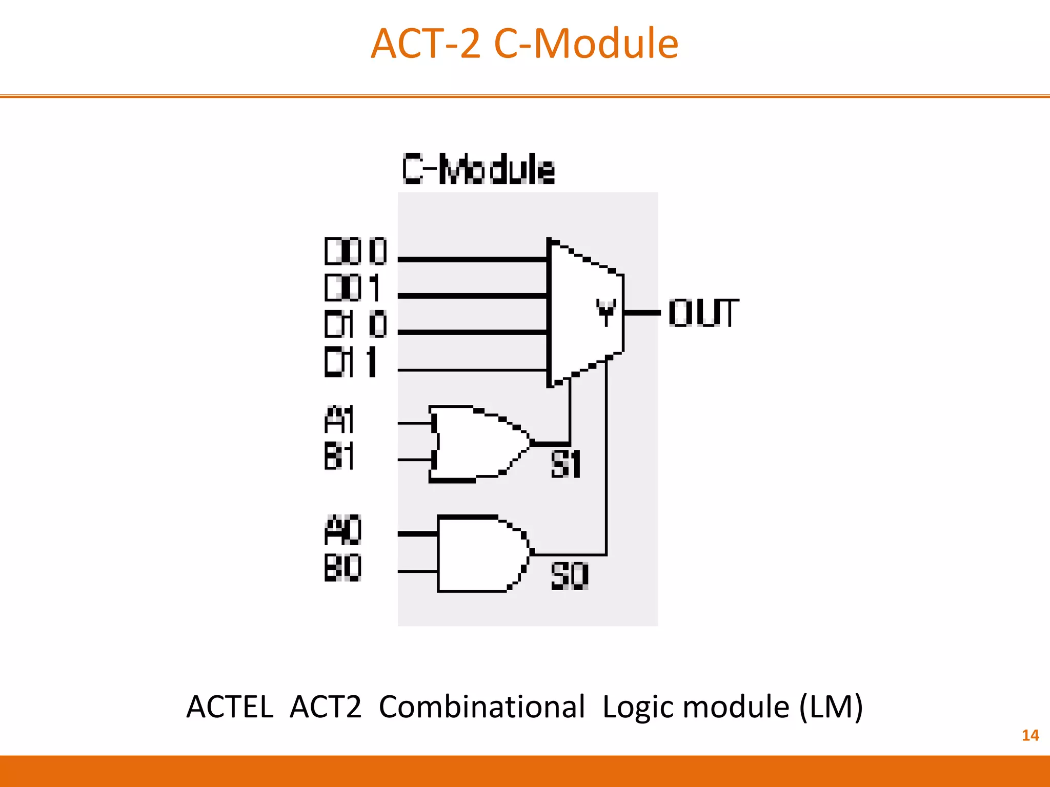
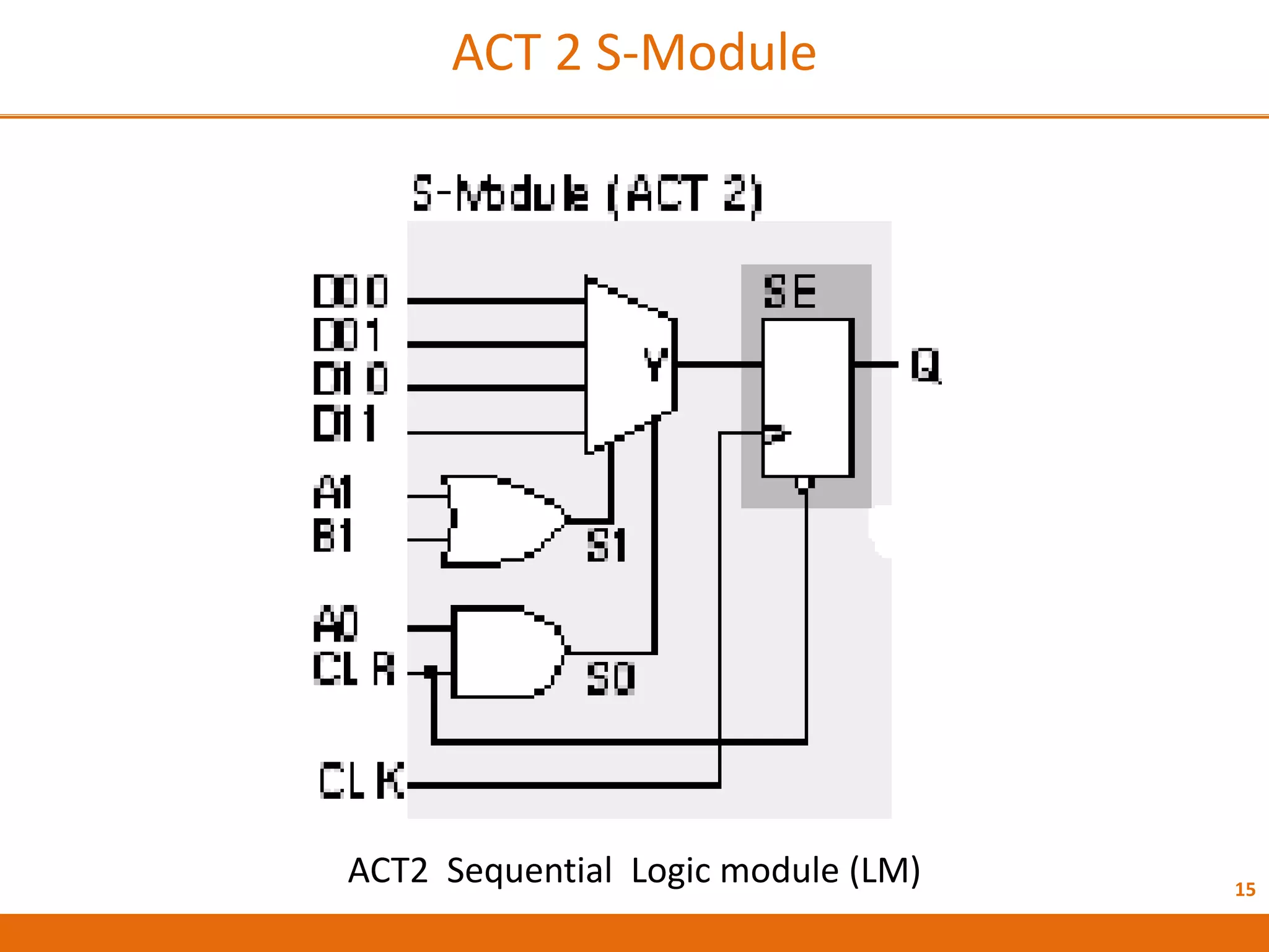
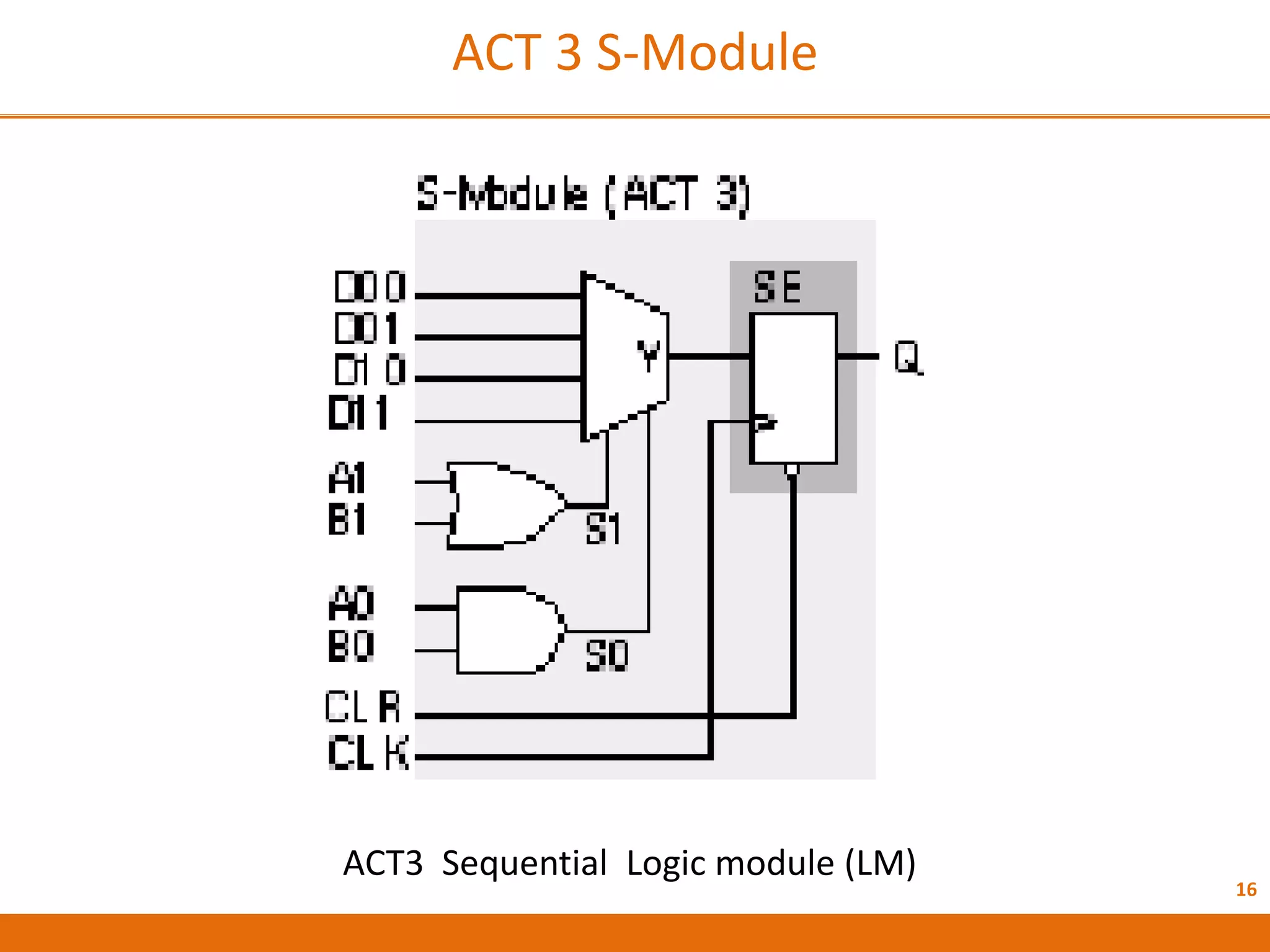
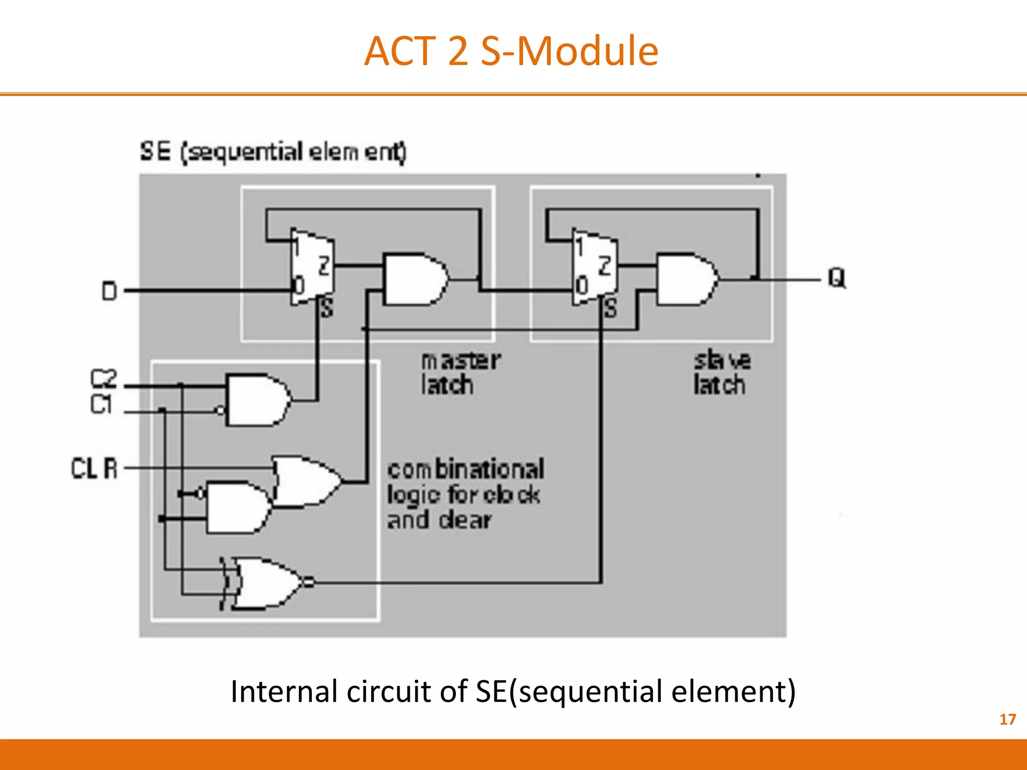
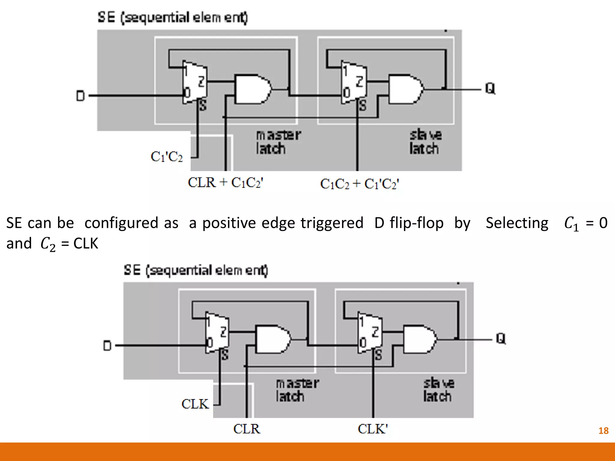
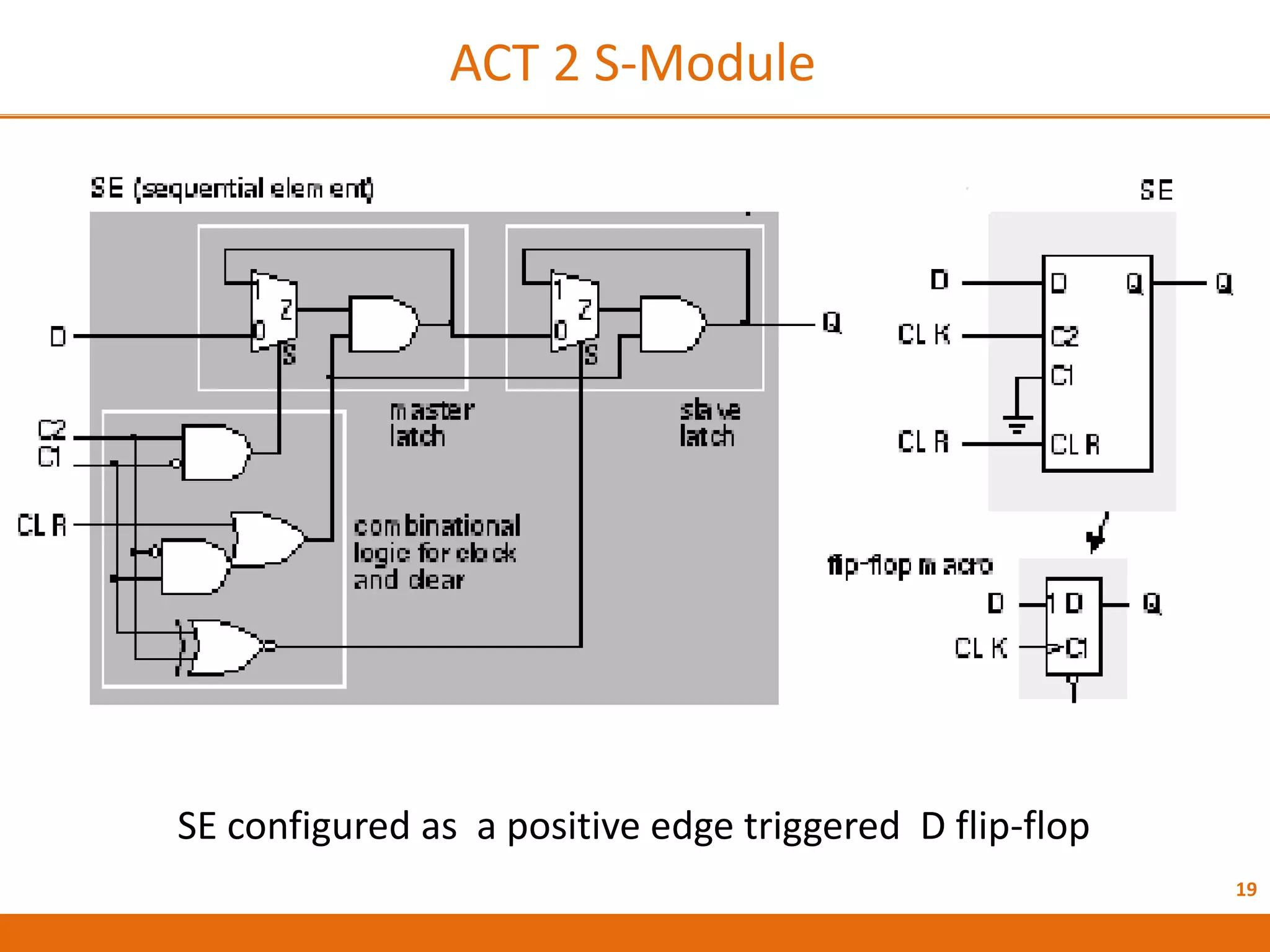


The document discusses Field Programmable Gate Arrays (FPGAs) and compares them to Application-Specific Integrated Circuits (ASICs), highlighting advantages such as quick configuration and reconfigurability, and disadvantages like larger space requirements and slower performance compared to ASICs. It also details the architecture of FPGAs, including components such as configurable logic blocks and input/output blocks, and identifies two types of FPGAs: reprogrammable and one-time programmable. Additionally, it touches on Actel FPGAs, emphasizing their multiplexer-based logic cells and various logic modules.