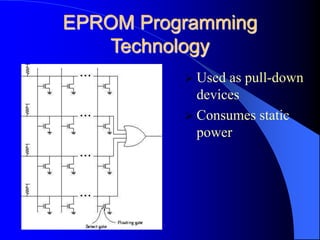
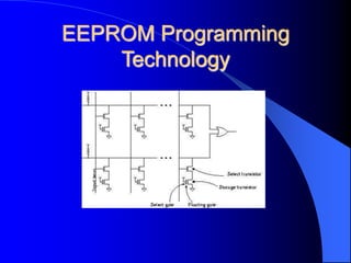
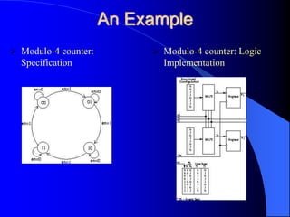
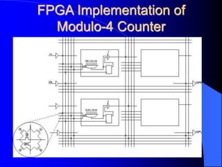
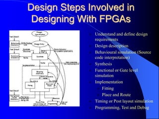
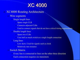
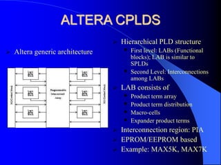
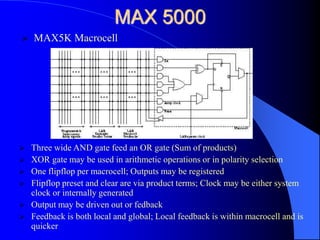
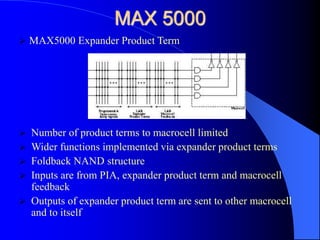
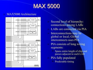
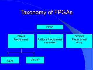
SlideShare a Scribd company logo
FPGA Architecture
Mrs.S.Priyatharsini
AP/ECE
KIT-CBE
Presentation Overview
 Available choice for digital designer
 FPGA – A detailed look
 Interconnection Framework
 FPGAs and CPLDs
 Field programmability and programming
technologies
 SRAM, Anti-fuse, EPROM and EEPROM
 Design steps
 Commercially available devices
 Xilinx XC4000
 Altera MAX 5000
Designer’s Choice
 Digital designer has various options
 SSI (small scale integrated circuits) or MSI (medium scale
integrated circuits) components
 Difficulties arises as design size increases
 Interconnections grow with complexity resulting in a
prolonged testing phase
 Simple programmable logic devices
 PALs (programmable array logic)
 PLAs (programmable logic array)
 Architecture not scalable; Power consumption and delays play
an important role in extending the architecture to complex
designs
 Implementation of larger designs leads to same difficulty as
that of discrete components
Designer’s Choice
 Quest for high capacity; Two choices
available
 MPGA (Masked Programmable Logic Devices)
 Customized during fabrication
 Low volume expensive
 Prolonged time-to-market and high financial risk
 FPGA (Field Programmable Logic Devices)
 Customized by end user
 Implements multi-level logic function
 Fast time to market and low risk
FPGA – A Quick Look
 Two dimensional array of customizable logic
block placed in an interconnect array
 Like PLDs programmable at users site
 Like MPGAs, implements thousands of gates of
logic in a single device
 Employs logic and interconnect structure capable of
implementing multi-level logic
 Scalable in proportion with logic removing many of the size
limitations of PLD derived two level architecture
 FPGAs offer the benefit of both MPGAs and
PLDs!
FPGA – A Detailed Look
 Based on the principle of functional completeness
 FPGA: Functionally complete elements (Logic
Blocks) placed in an interconnect framework
 Interconnection framework comprises of wire
segments and switches; Provide a means to
interconnect logic blocks
 Circuits are partitioned to logic block size,
mapped and routed
A Fictitious FPGA Architecture
(With Multiplexer As Functionally Complete Cell)
 Basic building block
Interconnection Framework
 Granularity and interconnection structure
has caused a split in the industry
 FPGA
– Fine grained
– Variable length
interconnect segments
– Timing in general is not
predictable; Timing
extracted after placement
and route
Interconnection Framework
 CPLD
– Coarse grained
(SPLD like blocks)
– Programmable crossbar
interconnect structure
– Interconnect structure uses
continuous metal lines
– The switch matrix may or may not
be fully populated
– Timing predictable if fully
populated
– Architecture does not scale well
Field Programmability
 Field programmability is achieved through
switches (Transistors controlled by memory
elements or fuses)
 Switches control the following aspects
 Interconnection among wire segments
 Configuration of logic blocks
 Distributed memory elements controlling the
switches and configuration of logic blocks are
together called “Configuration Memory”
Technology of Programmable
Elements
 Vary from vendor to vendor. All share the
common property: Configurable in one of the two
positions – ‘ON’ or ‘OFF’
 Can be classified into three categories:
 SRAM based
 Fuse based
 EPROM/EEPROM/Flash based
 Desired properties:
 Minimum area consumption
 Low on resistance; High off resistance
 Low parasitic capacitance to the attached wire
 Reliability in volume production
SRAM Programming
Technology
 Employs SRAM (Static RAM) cells
to control pass transistors and/or
transmission gates
 SRAM cells control the configuration
of logic block as well
 Volatile
 Needs an external storage
 Needs a power-on configuration
mechanism
 In-circuit re-programmable
 Lesser configuration time
 Occupies relatively larger area
Anti-fuse Programming
Technology
 Though implementation differ, all anti-fuse
programming elements share common property
 Uses materials which normally resides in high
impedance state
 But can be fused irreversibly into low impedance state
by applying high voltage
Anti-fuse Programming
Technology
 Very low ON Resistance (Faster implementation
of circuits)
 Limited size of anti-fuse elements; Interconnects
occupy relatively lesser area
 Offset : Larger transistors needed for programming
 One Time Programmable
 Cannot be re-programmed
 (Design changes are not possible)
 Retain configuration after power off
EPROM, EEPROM or Flash
Based Programming Technology
 EPROM Programming Technology
 Two gates: Floating and Select
 Normal mode:
 No charge on floating gate
 Transistor behaves as normal n-channel transistor
 Floating gate charged by applying high voltage
 Threshold of transistor (as seen by gate) increases
 Transistor turned off permanently
 Re-programmable by exposing to UV radiation
EPROM Programming
Technology
 Used as pull-down
devices
 Consumes static
power
EPROM Programming
Technology
 No external storage mechanism
 Re-programmable (Not all!)
 Not in-system re-programmable
 Re-programming is a time consuming task
EEPROM Programming
Technology
 Two gates: Floating and Select
 Functionally equivalent to EPROM; Construction
and structure differ
 Electrically Erasable: Re-programmable by
applying high voltage
(No UV radiation expose!)
 When un-programmed, the threshold (as seen by
select gate) is negative!
EEPROM Programming
Technology
EEPROM Programming
Technology
 Re-programmable; In general, in-system re-
programmable
 Re-programming consumes lesser time
compared to EPROM technology
 Multiple voltage sources may be required
 Area occupied is twice that of EPROM!
An Example
 Modulo-4 counter:
Specification
 Modulo-4 counter: Logic
Implementation
FPGA Implementation of
Modulo-4 Counter
Design Steps Involved in
Designing With FPGAs
 Understand and define design
requirements
 Design description
 Behavioural simulation (Source
code interpretation)
 Synthesis
 Functional or Gate level
simulation
 Implementation
 Fitting
 Place and Route
 Timing or Post layout simulation
 Programming, Test and Debug
Commercially Available
Devices
 Architecture differs from vendor to vendor
 Characterized by
 Structure and content of logic block
 Structure and content of routing resources
 To examine, look at some of available
devices
 FPGA: Xilinx (XC4000)
 CPLD: Altera (MAX 5K)
Xilinx FPGAs
 Symmetric Array based; Array
consists of CLBs with LUTs
and D-Flipflops
 N-input LUTs can implement
any n-input boolean function
 Array embedded within the
periphery of IO blocks
 Array elements interleaved with
routing resources (wire
segments, switch matrix and
single connection points)
 Employs SRAM technology
 Generic Xilinx Architecture
XC 4000
 XC4000 CLB
 3 LUTs and 2 Flip-flops in a
two stage arrangement
 2 Outputs: Can be registered or
combinational
 External signals can also be
registered
 More of internal signals are
available for connections
 Can implement any two
independent functions of four
variables or any single function
of five variables
XC4000
 XC4000 Routing Architecture
XC 4000
 XC4000 Routing Architecture
 Wire segments
 Single length lines
 Spans single CLB
 Connects adjacent CLBs
 Used to connect signals that do not have critical timing requirements
 Double length lines
 Spans two CLBs
 Uses half as much switch as a single length connection
 Long lines
 Low skew; Used for signals such as clock
 Relatively rare resource
 Switch Matrix
 Every line is connected to lines on the other three direction
 Each connection requires six transistors
ALTERA CPLDS
 Hierarchical PLD structure
 First level: LABs (Functional
blocks); LAB is similar to
SPLDs
 Second Level: Interconnections
among LABs
 LAB consists of
 Product term array
 Product term distribution
 Macro-cells
 Expander product terms
 Interconnection region: PIA
 EPROM/EEPROM based
 Example: MAX5K, MAX7K
 Altera generic architecture
MAX 5000
 Three wide AND gate feed an OR gate (Sum of products)
 XOR gate may be used in arithmetic operations or in polarity selection
 One flipflop per macrocell; Outputs may be registered
 Flipflop preset and clear are via product terms; Clock may be either system
clock or internally generated
 Output may be driven out or fedback
 Feedback is both local and global; Local feedback is within macrocell and is
quicker
 MAX5K Macrocell
MAX 5000
 Number of product terms to macrocell limited
 Wider functions implemented via expander product terms
 Foldback NAND structure
 Inputs are from PIA, expander product term and macrocell
feedback
 Outputs of expander product term are sent to other macrocell
and to itself
 MAX5000 Expander Product Term
MAX 5000
 Second level of hierarchy:
connections among LABs
 LABs are connected via PIA
 Interconnections may be
global or local; Global
interconnects uses PIA
 PIA consists of long wiring
segments:
 Spans entire length of chip and
passes adjacent to each LAB
 PIA fully populated
 Predictable timing
 MAX5000 Architecture
SRAM FPGA -- EEPROM
FPGA
 An FPGA is similar to several other types of
devices which have been around for quite a
while, the difference being that an FPGA is
simply much more expandable and versatile.
The devices which FPGAs get compared to
most often are CPLDs (Complex
Programmable Logic Devices), which are
similar in function but typically have way less
logic gates inside them; Customizable CPU
design is much more feasible with an FPGA.
Once upon a time, CPLDs also had the
distinct advantage of retaining their
SRAM FPGA -- EEPROM
FPGA
 when turned off; When FPGAs first came out,
they used simple SRAM to hold their
configuration, which of course would be lost
when the device lost power. Back then, the
FPGA had to be programmed from scratch
every time it was turned on, usually from a
separate serial ROM chip. But today, FPGAs
come in Flash, EPROM, and EEPROM
variants, which will retain configuration, and
which can also be re-programmed. (Fuse
and anti-fuse FPGAs also exist, which act
like PROMs in that they are one-time
SRAM FPGA -- EEPROM
FPGA
 afterward.) Despite this, however, most
FPGAs still use SRAM for reasons of
simplicity (when you need to reprogram it, it's
easier to re-encode a small ROM chip than to
reprogram a large FPGA chip), so count on
having to use a separate boot ROM for the
FPGA.
 Use of an FPGA is broadly divided into two
main stages: The first is "configuration
mode", the mode in which the FPGA is when
you first power it up. Configuration mode is,
as you may have guessed, where you
SRAM FPGA -- EEPROM
FPGA
 this is when you load your code into it,
dictating how the pins behave. Once
configuration is complete, the FPGA
goes into "user mode", its main mode of
operation, where the programmed
circuit actually starts functioning.
Product – FPGA vs ASIC
Comparison:
 FPGA benefits vs ASICs:
- Design time: 9 month design cycle vs 2-3 years
- Cost: No $3-5 M upfront (NRE) design cost.
No $100-500K mask-set cost
- Volume: High initial ASIC cost recovered only in very high volume products
 Due to Moore’s law, many ASIC market requirements now met by FPGAs
- Eg. Virtex II Pro has 4 processors, 10 Mb memory, IO
Resulting Market Shift:
 Dramatic decline in number of ASIC design starts:
- 11,000 in ’97
- 1,500 in ’02
 FPGAs as a % of Logic market:
- Increase from 10 to 22% in past 3-4 years
 FPGAs (or programmable logic) is the fastest growing segment of the
semiconductor industry!!
FPGA/ASIC Crossover Changes
Production Volume
Cost
FPGA Cost Advantage ASIC Cost Advantage
FPGA Cost Advantage
Taxonomy of FPGAs
Island Cellular
SRAM
Programmed Antifuse Programmed
channeled
EPROM
Programmed
Array
FPGA

More Related Content

Similar to FPGA-Architecture.ppt

Technical Seminar.pptx
Technical Seminar.pptxTechnical Seminar.pptx
Technical Seminar.pptx
VaishnaviRavella
 
L12_PROGRAMMABLE+LOGIC+DEVICES+(PLD).ppt
L12_PROGRAMMABLE+LOGIC+DEVICES+(PLD).pptL12_PROGRAMMABLE+LOGIC+DEVICES+(PLD).ppt
L12_PROGRAMMABLE+LOGIC+DEVICES+(PLD).ppt
MikeTango5
 
L12 programmable+logic+devices+(pld)
L12 programmable+logic+devices+(pld)L12 programmable+logic+devices+(pld)
L12 programmable+logic+devices+(pld)
NAGASAI547
 
Fundamentals of FPGA
Fundamentals of FPGAFundamentals of FPGA
Fundamentals of FPGA
velamakuri
 
Fpg as 11 body
Fpg as 11 bodyFpg as 11 body
Fpg as 11 body
Rameez Raja
 
Digital System Design-Introductio to ASIC
Digital System Design-Introductio to ASICDigital System Design-Introductio to ASIC
Digital System Design-Introductio to ASIC
Indira Priyadarshini
 
programmable_devices_en_02_2014
programmable_devices_en_02_2014programmable_devices_en_02_2014
programmable_devices_en_02_2014Svetozar Jovanovic
 
Fpga lecture
Fpga lectureFpga lecture
Fpga lecture
Zhwan Rashid
 
Digital Systems Design
Digital Systems DesignDigital Systems Design
Digital Systems Design
Reza Sameni
 
Fpga based motor controller
Fpga based motor controllerFpga based motor controller
Fpga based motor controller
Uday Wankar
 
Chapter 4
Chapter 4Chapter 4
Chapter 4
Sunil Kumar
 
1. FPGA architectures.pdf
1. FPGA architectures.pdf1. FPGA architectures.pdf
1. FPGA architectures.pdf
TesfuFiseha1
 
module 1-2 - Design Methods, parameters and examples.pptx
module 1-2 - Design Methods, parameters and examples.pptxmodule 1-2 - Design Methods, parameters and examples.pptx
module 1-2 - Design Methods, parameters and examples.pptx
Maaz609108
 
Embedded systems-unit-1
Embedded systems-unit-1Embedded systems-unit-1
Embedded systems-unit-1
Prabhu Mali
 
Iaetsd a design of fpga with ledr encoding and
Iaetsd a design of fpga with ledr encoding andIaetsd a design of fpga with ledr encoding and
Iaetsd a design of fpga with ledr encoding and
Iaetsd Iaetsd
 
Convolution
ConvolutionConvolution
Convolution
sridharbommu
 
Fpga optimus main_print
Fpga optimus  main_printFpga optimus  main_print
Fpga optimus main_printSushant Burde
 
Implementation strategies for digital ics
Implementation strategies for digital icsImplementation strategies for digital ics
Implementation strategies for digital ics
aroosa khan
 
AN DYNAMIC ENERGY MANAGEMENT ON FPGA FOR WIRELESS SENSOR NETWORK
AN DYNAMIC ENERGY MANAGEMENT ON FPGA FOR WIRELESS SENSOR NETWORKAN DYNAMIC ENERGY MANAGEMENT ON FPGA FOR WIRELESS SENSOR NETWORK
AN DYNAMIC ENERGY MANAGEMENT ON FPGA FOR WIRELESS SENSOR NETWORK
csijjournal
 

Similar to FPGA-Architecture.ppt (20)

Technical Seminar.pptx
Technical Seminar.pptxTechnical Seminar.pptx
Technical Seminar.pptx
 
L12_PROGRAMMABLE+LOGIC+DEVICES+(PLD).ppt
L12_PROGRAMMABLE+LOGIC+DEVICES+(PLD).pptL12_PROGRAMMABLE+LOGIC+DEVICES+(PLD).ppt
L12_PROGRAMMABLE+LOGIC+DEVICES+(PLD).ppt
 
L12 programmable+logic+devices+(pld)
L12 programmable+logic+devices+(pld)L12 programmable+logic+devices+(pld)
L12 programmable+logic+devices+(pld)
 
Fundamentals of FPGA
Fundamentals of FPGAFundamentals of FPGA
Fundamentals of FPGA
 
Fpg as 11 body
Fpg as 11 bodyFpg as 11 body
Fpg as 11 body
 
Asic
AsicAsic
Asic
 
Digital System Design-Introductio to ASIC
Digital System Design-Introductio to ASICDigital System Design-Introductio to ASIC
Digital System Design-Introductio to ASIC
 
programmable_devices_en_02_2014
programmable_devices_en_02_2014programmable_devices_en_02_2014
programmable_devices_en_02_2014
 
Fpga lecture
Fpga lectureFpga lecture
Fpga lecture
 
Digital Systems Design
Digital Systems DesignDigital Systems Design
Digital Systems Design
 
Fpga based motor controller
Fpga based motor controllerFpga based motor controller
Fpga based motor controller
 
Chapter 4
Chapter 4Chapter 4
Chapter 4
 
1. FPGA architectures.pdf
1. FPGA architectures.pdf1. FPGA architectures.pdf
1. FPGA architectures.pdf
 
module 1-2 - Design Methods, parameters and examples.pptx
module 1-2 - Design Methods, parameters and examples.pptxmodule 1-2 - Design Methods, parameters and examples.pptx
module 1-2 - Design Methods, parameters and examples.pptx
 
Embedded systems-unit-1
Embedded systems-unit-1Embedded systems-unit-1
Embedded systems-unit-1
 
Iaetsd a design of fpga with ledr encoding and
Iaetsd a design of fpga with ledr encoding andIaetsd a design of fpga with ledr encoding and
Iaetsd a design of fpga with ledr encoding and
 
Convolution
ConvolutionConvolution
Convolution
 
Fpga optimus main_print
Fpga optimus  main_printFpga optimus  main_print
Fpga optimus main_print
 
Implementation strategies for digital ics
Implementation strategies for digital icsImplementation strategies for digital ics
Implementation strategies for digital ics
 
AN DYNAMIC ENERGY MANAGEMENT ON FPGA FOR WIRELESS SENSOR NETWORK
AN DYNAMIC ENERGY MANAGEMENT ON FPGA FOR WIRELESS SENSOR NETWORKAN DYNAMIC ENERGY MANAGEMENT ON FPGA FOR WIRELESS SENSOR NETWORK
AN DYNAMIC ENERGY MANAGEMENT ON FPGA FOR WIRELESS SENSOR NETWORK
 

Recently uploaded

Final project report on grocery store management system..pdf
Final project report on grocery store management system..pdfFinal project report on grocery store management system..pdf
Final project report on grocery store management system..pdf
Kamal Acharya
 
Pile Foundation by Venkatesh Taduvai (Sub Geotechnical Engineering II)-conver...
Pile Foundation by Venkatesh Taduvai (Sub Geotechnical Engineering II)-conver...Pile Foundation by Venkatesh Taduvai (Sub Geotechnical Engineering II)-conver...
Pile Foundation by Venkatesh Taduvai (Sub Geotechnical Engineering II)-conver...
AJAYKUMARPUND1
 
Hybrid optimization of pumped hydro system and solar- Engr. Abdul-Azeez.pdf
Hybrid optimization of pumped hydro system and solar- Engr. Abdul-Azeez.pdfHybrid optimization of pumped hydro system and solar- Engr. Abdul-Azeez.pdf
Hybrid optimization of pumped hydro system and solar- Engr. Abdul-Azeez.pdf
fxintegritypublishin
 
NO1 Uk best vashikaran specialist in delhi vashikaran baba near me online vas...
NO1 Uk best vashikaran specialist in delhi vashikaran baba near me online vas...NO1 Uk best vashikaran specialist in delhi vashikaran baba near me online vas...
NO1 Uk best vashikaran specialist in delhi vashikaran baba near me online vas...
Amil Baba Dawood bangali
 
Investor-Presentation-Q1FY2024 investor presentation document.pptx
Investor-Presentation-Q1FY2024 investor presentation document.pptxInvestor-Presentation-Q1FY2024 investor presentation document.pptx
Investor-Presentation-Q1FY2024 investor presentation document.pptx
AmarGB2
 
6th International Conference on Machine Learning & Applications (CMLA 2024)
6th International Conference on Machine Learning & Applications (CMLA 2024)6th International Conference on Machine Learning & Applications (CMLA 2024)
6th International Conference on Machine Learning & Applications (CMLA 2024)
ClaraZara1
 
Water Industry Process Automation and Control Monthly - May 2024.pdf
Water Industry Process Automation and Control Monthly - May 2024.pdfWater Industry Process Automation and Control Monthly - May 2024.pdf
Water Industry Process Automation and Control Monthly - May 2024.pdf
Water Industry Process Automation & Control
 
Recycled Concrete Aggregate in Construction Part III
Recycled Concrete Aggregate in Construction Part IIIRecycled Concrete Aggregate in Construction Part III
Recycled Concrete Aggregate in Construction Part III
Aditya Rajan Patra
 
space technology lecture notes on satellite
space technology lecture notes on satellitespace technology lecture notes on satellite
space technology lecture notes on satellite
ongomchris
 
Governing Equations for Fundamental Aerodynamics_Anderson2010.pdf
Governing Equations for Fundamental Aerodynamics_Anderson2010.pdfGoverning Equations for Fundamental Aerodynamics_Anderson2010.pdf
Governing Equations for Fundamental Aerodynamics_Anderson2010.pdf
WENKENLI1
 
Heap Sort (SS).ppt FOR ENGINEERING GRADUATES, BCA, MCA, MTECH, BSC STUDENTS
Heap Sort (SS).ppt FOR ENGINEERING GRADUATES, BCA, MCA, MTECH, BSC STUDENTSHeap Sort (SS).ppt FOR ENGINEERING GRADUATES, BCA, MCA, MTECH, BSC STUDENTS
Heap Sort (SS).ppt FOR ENGINEERING GRADUATES, BCA, MCA, MTECH, BSC STUDENTS
Soumen Santra
 
HYDROPOWER - Hydroelectric power generation
HYDROPOWER - Hydroelectric power generationHYDROPOWER - Hydroelectric power generation
HYDROPOWER - Hydroelectric power generation
Robbie Edward Sayers
 
Standard Reomte Control Interface - Neometrix
Standard Reomte Control Interface - NeometrixStandard Reomte Control Interface - Neometrix
Standard Reomte Control Interface - Neometrix
Neometrix_Engineering_Pvt_Ltd
 
block diagram and signal flow graph representation
block diagram and signal flow graph representationblock diagram and signal flow graph representation
block diagram and signal flow graph representation
Divya Somashekar
 
Unbalanced Three Phase Systems and circuits.pptx
Unbalanced Three Phase Systems and circuits.pptxUnbalanced Three Phase Systems and circuits.pptx
Unbalanced Three Phase Systems and circuits.pptx
ChristineTorrepenida1
 
Basic Industrial Engineering terms for apparel
Basic Industrial Engineering terms for apparelBasic Industrial Engineering terms for apparel
Basic Industrial Engineering terms for apparel
top1002
 
Forklift Classes Overview by Intella Parts
Forklift Classes Overview by Intella PartsForklift Classes Overview by Intella Parts
Forklift Classes Overview by Intella Parts
Intella Parts
 
一比一原版(IIT毕业证)伊利诺伊理工大学毕业证成绩单专业办理
一比一原版(IIT毕业证)伊利诺伊理工大学毕业证成绩单专业办理一比一原版(IIT毕业证)伊利诺伊理工大学毕业证成绩单专业办理
一比一原版(IIT毕业证)伊利诺伊理工大学毕业证成绩单专业办理
zwunae
 
DfMAy 2024 - key insights and contributions
DfMAy 2024 - key insights and contributionsDfMAy 2024 - key insights and contributions
DfMAy 2024 - key insights and contributions
gestioneergodomus
 
NUMERICAL SIMULATIONS OF HEAT AND MASS TRANSFER IN CONDENSING HEAT EXCHANGERS...
NUMERICAL SIMULATIONS OF HEAT AND MASS TRANSFER IN CONDENSING HEAT EXCHANGERS...NUMERICAL SIMULATIONS OF HEAT AND MASS TRANSFER IN CONDENSING HEAT EXCHANGERS...
NUMERICAL SIMULATIONS OF HEAT AND MASS TRANSFER IN CONDENSING HEAT EXCHANGERS...
ssuser7dcef0
 

Recently uploaded (20)

Final project report on grocery store management system..pdf
Final project report on grocery store management system..pdfFinal project report on grocery store management system..pdf
Final project report on grocery store management system..pdf
 
Pile Foundation by Venkatesh Taduvai (Sub Geotechnical Engineering II)-conver...
Pile Foundation by Venkatesh Taduvai (Sub Geotechnical Engineering II)-conver...Pile Foundation by Venkatesh Taduvai (Sub Geotechnical Engineering II)-conver...
Pile Foundation by Venkatesh Taduvai (Sub Geotechnical Engineering II)-conver...
 
Hybrid optimization of pumped hydro system and solar- Engr. Abdul-Azeez.pdf
Hybrid optimization of pumped hydro system and solar- Engr. Abdul-Azeez.pdfHybrid optimization of pumped hydro system and solar- Engr. Abdul-Azeez.pdf
Hybrid optimization of pumped hydro system and solar- Engr. Abdul-Azeez.pdf
 
NO1 Uk best vashikaran specialist in delhi vashikaran baba near me online vas...
NO1 Uk best vashikaran specialist in delhi vashikaran baba near me online vas...NO1 Uk best vashikaran specialist in delhi vashikaran baba near me online vas...
NO1 Uk best vashikaran specialist in delhi vashikaran baba near me online vas...
 
Investor-Presentation-Q1FY2024 investor presentation document.pptx
Investor-Presentation-Q1FY2024 investor presentation document.pptxInvestor-Presentation-Q1FY2024 investor presentation document.pptx
Investor-Presentation-Q1FY2024 investor presentation document.pptx
 
6th International Conference on Machine Learning & Applications (CMLA 2024)
6th International Conference on Machine Learning & Applications (CMLA 2024)6th International Conference on Machine Learning & Applications (CMLA 2024)
6th International Conference on Machine Learning & Applications (CMLA 2024)
 
Water Industry Process Automation and Control Monthly - May 2024.pdf
Water Industry Process Automation and Control Monthly - May 2024.pdfWater Industry Process Automation and Control Monthly - May 2024.pdf
Water Industry Process Automation and Control Monthly - May 2024.pdf
 
Recycled Concrete Aggregate in Construction Part III
Recycled Concrete Aggregate in Construction Part IIIRecycled Concrete Aggregate in Construction Part III
Recycled Concrete Aggregate in Construction Part III
 
space technology lecture notes on satellite
space technology lecture notes on satellitespace technology lecture notes on satellite
space technology lecture notes on satellite
 
Governing Equations for Fundamental Aerodynamics_Anderson2010.pdf
Governing Equations for Fundamental Aerodynamics_Anderson2010.pdfGoverning Equations for Fundamental Aerodynamics_Anderson2010.pdf
Governing Equations for Fundamental Aerodynamics_Anderson2010.pdf
 
Heap Sort (SS).ppt FOR ENGINEERING GRADUATES, BCA, MCA, MTECH, BSC STUDENTS
Heap Sort (SS).ppt FOR ENGINEERING GRADUATES, BCA, MCA, MTECH, BSC STUDENTSHeap Sort (SS).ppt FOR ENGINEERING GRADUATES, BCA, MCA, MTECH, BSC STUDENTS
Heap Sort (SS).ppt FOR ENGINEERING GRADUATES, BCA, MCA, MTECH, BSC STUDENTS
 
HYDROPOWER - Hydroelectric power generation
HYDROPOWER - Hydroelectric power generationHYDROPOWER - Hydroelectric power generation
HYDROPOWER - Hydroelectric power generation
 
Standard Reomte Control Interface - Neometrix
Standard Reomte Control Interface - NeometrixStandard Reomte Control Interface - Neometrix
Standard Reomte Control Interface - Neometrix
 
block diagram and signal flow graph representation
block diagram and signal flow graph representationblock diagram and signal flow graph representation
block diagram and signal flow graph representation
 
Unbalanced Three Phase Systems and circuits.pptx
Unbalanced Three Phase Systems and circuits.pptxUnbalanced Three Phase Systems and circuits.pptx
Unbalanced Three Phase Systems and circuits.pptx
 
Basic Industrial Engineering terms for apparel
Basic Industrial Engineering terms for apparelBasic Industrial Engineering terms for apparel
Basic Industrial Engineering terms for apparel
 
Forklift Classes Overview by Intella Parts
Forklift Classes Overview by Intella PartsForklift Classes Overview by Intella Parts
Forklift Classes Overview by Intella Parts
 
一比一原版(IIT毕业证)伊利诺伊理工大学毕业证成绩单专业办理
一比一原版(IIT毕业证)伊利诺伊理工大学毕业证成绩单专业办理一比一原版(IIT毕业证)伊利诺伊理工大学毕业证成绩单专业办理
一比一原版(IIT毕业证)伊利诺伊理工大学毕业证成绩单专业办理
 
DfMAy 2024 - key insights and contributions
DfMAy 2024 - key insights and contributionsDfMAy 2024 - key insights and contributions
DfMAy 2024 - key insights and contributions
 
NUMERICAL SIMULATIONS OF HEAT AND MASS TRANSFER IN CONDENSING HEAT EXCHANGERS...
NUMERICAL SIMULATIONS OF HEAT AND MASS TRANSFER IN CONDENSING HEAT EXCHANGERS...NUMERICAL SIMULATIONS OF HEAT AND MASS TRANSFER IN CONDENSING HEAT EXCHANGERS...
NUMERICAL SIMULATIONS OF HEAT AND MASS TRANSFER IN CONDENSING HEAT EXCHANGERS...
 

FPGA-Architecture.ppt

  • 2. Presentation Overview  Available choice for digital designer  FPGA – A detailed look  Interconnection Framework  FPGAs and CPLDs  Field programmability and programming technologies  SRAM, Anti-fuse, EPROM and EEPROM  Design steps  Commercially available devices  Xilinx XC4000  Altera MAX 5000
  • 3. Designer’s Choice  Digital designer has various options  SSI (small scale integrated circuits) or MSI (medium scale integrated circuits) components  Difficulties arises as design size increases  Interconnections grow with complexity resulting in a prolonged testing phase  Simple programmable logic devices  PALs (programmable array logic)  PLAs (programmable logic array)  Architecture not scalable; Power consumption and delays play an important role in extending the architecture to complex designs  Implementation of larger designs leads to same difficulty as that of discrete components
  • 4. Designer’s Choice  Quest for high capacity; Two choices available  MPGA (Masked Programmable Logic Devices)  Customized during fabrication  Low volume expensive  Prolonged time-to-market and high financial risk  FPGA (Field Programmable Logic Devices)  Customized by end user  Implements multi-level logic function  Fast time to market and low risk
  • 5. FPGA – A Quick Look  Two dimensional array of customizable logic block placed in an interconnect array  Like PLDs programmable at users site  Like MPGAs, implements thousands of gates of logic in a single device  Employs logic and interconnect structure capable of implementing multi-level logic  Scalable in proportion with logic removing many of the size limitations of PLD derived two level architecture  FPGAs offer the benefit of both MPGAs and PLDs!
  • 6. FPGA – A Detailed Look  Based on the principle of functional completeness  FPGA: Functionally complete elements (Logic Blocks) placed in an interconnect framework  Interconnection framework comprises of wire segments and switches; Provide a means to interconnect logic blocks  Circuits are partitioned to logic block size, mapped and routed
  • 7. A Fictitious FPGA Architecture (With Multiplexer As Functionally Complete Cell)  Basic building block
  • 8. Interconnection Framework  Granularity and interconnection structure has caused a split in the industry  FPGA – Fine grained – Variable length interconnect segments – Timing in general is not predictable; Timing extracted after placement and route
  • 9. Interconnection Framework  CPLD – Coarse grained (SPLD like blocks) – Programmable crossbar interconnect structure – Interconnect structure uses continuous metal lines – The switch matrix may or may not be fully populated – Timing predictable if fully populated – Architecture does not scale well
  • 10. Field Programmability  Field programmability is achieved through switches (Transistors controlled by memory elements or fuses)  Switches control the following aspects  Interconnection among wire segments  Configuration of logic blocks  Distributed memory elements controlling the switches and configuration of logic blocks are together called “Configuration Memory”
  • 11. Technology of Programmable Elements  Vary from vendor to vendor. All share the common property: Configurable in one of the two positions – ‘ON’ or ‘OFF’  Can be classified into three categories:  SRAM based  Fuse based  EPROM/EEPROM/Flash based  Desired properties:  Minimum area consumption  Low on resistance; High off resistance  Low parasitic capacitance to the attached wire  Reliability in volume production
  • 12. SRAM Programming Technology  Employs SRAM (Static RAM) cells to control pass transistors and/or transmission gates  SRAM cells control the configuration of logic block as well  Volatile  Needs an external storage  Needs a power-on configuration mechanism  In-circuit re-programmable  Lesser configuration time  Occupies relatively larger area
  • 13. Anti-fuse Programming Technology  Though implementation differ, all anti-fuse programming elements share common property  Uses materials which normally resides in high impedance state  But can be fused irreversibly into low impedance state by applying high voltage
  • 14. Anti-fuse Programming Technology  Very low ON Resistance (Faster implementation of circuits)  Limited size of anti-fuse elements; Interconnects occupy relatively lesser area  Offset : Larger transistors needed for programming  One Time Programmable  Cannot be re-programmed  (Design changes are not possible)  Retain configuration after power off
  • 15. EPROM, EEPROM or Flash Based Programming Technology  EPROM Programming Technology  Two gates: Floating and Select  Normal mode:  No charge on floating gate  Transistor behaves as normal n-channel transistor  Floating gate charged by applying high voltage  Threshold of transistor (as seen by gate) increases  Transistor turned off permanently  Re-programmable by exposing to UV radiation
  • 16. EPROM Programming Technology  Used as pull-down devices  Consumes static power
  • 17. EPROM Programming Technology  No external storage mechanism  Re-programmable (Not all!)  Not in-system re-programmable  Re-programming is a time consuming task
  • 18. EEPROM Programming Technology  Two gates: Floating and Select  Functionally equivalent to EPROM; Construction and structure differ  Electrically Erasable: Re-programmable by applying high voltage (No UV radiation expose!)  When un-programmed, the threshold (as seen by select gate) is negative!
  • 20. EEPROM Programming Technology  Re-programmable; In general, in-system re- programmable  Re-programming consumes lesser time compared to EPROM technology  Multiple voltage sources may be required  Area occupied is twice that of EPROM!
  • 21. An Example  Modulo-4 counter: Specification  Modulo-4 counter: Logic Implementation
  • 23. Design Steps Involved in Designing With FPGAs  Understand and define design requirements  Design description  Behavioural simulation (Source code interpretation)  Synthesis  Functional or Gate level simulation  Implementation  Fitting  Place and Route  Timing or Post layout simulation  Programming, Test and Debug
  • 24. Commercially Available Devices  Architecture differs from vendor to vendor  Characterized by  Structure and content of logic block  Structure and content of routing resources  To examine, look at some of available devices  FPGA: Xilinx (XC4000)  CPLD: Altera (MAX 5K)
  • 25. Xilinx FPGAs  Symmetric Array based; Array consists of CLBs with LUTs and D-Flipflops  N-input LUTs can implement any n-input boolean function  Array embedded within the periphery of IO blocks  Array elements interleaved with routing resources (wire segments, switch matrix and single connection points)  Employs SRAM technology  Generic Xilinx Architecture
  • 26. XC 4000  XC4000 CLB  3 LUTs and 2 Flip-flops in a two stage arrangement  2 Outputs: Can be registered or combinational  External signals can also be registered  More of internal signals are available for connections  Can implement any two independent functions of four variables or any single function of five variables
  • 28. XC 4000  XC4000 Routing Architecture  Wire segments  Single length lines  Spans single CLB  Connects adjacent CLBs  Used to connect signals that do not have critical timing requirements  Double length lines  Spans two CLBs  Uses half as much switch as a single length connection  Long lines  Low skew; Used for signals such as clock  Relatively rare resource  Switch Matrix  Every line is connected to lines on the other three direction  Each connection requires six transistors
  • 29. ALTERA CPLDS  Hierarchical PLD structure  First level: LABs (Functional blocks); LAB is similar to SPLDs  Second Level: Interconnections among LABs  LAB consists of  Product term array  Product term distribution  Macro-cells  Expander product terms  Interconnection region: PIA  EPROM/EEPROM based  Example: MAX5K, MAX7K  Altera generic architecture
  • 30. MAX 5000  Three wide AND gate feed an OR gate (Sum of products)  XOR gate may be used in arithmetic operations or in polarity selection  One flipflop per macrocell; Outputs may be registered  Flipflop preset and clear are via product terms; Clock may be either system clock or internally generated  Output may be driven out or fedback  Feedback is both local and global; Local feedback is within macrocell and is quicker  MAX5K Macrocell
  • 31. MAX 5000  Number of product terms to macrocell limited  Wider functions implemented via expander product terms  Foldback NAND structure  Inputs are from PIA, expander product term and macrocell feedback  Outputs of expander product term are sent to other macrocell and to itself  MAX5000 Expander Product Term
  • 32. MAX 5000  Second level of hierarchy: connections among LABs  LABs are connected via PIA  Interconnections may be global or local; Global interconnects uses PIA  PIA consists of long wiring segments:  Spans entire length of chip and passes adjacent to each LAB  PIA fully populated  Predictable timing  MAX5000 Architecture
  • 33. SRAM FPGA -- EEPROM FPGA  An FPGA is similar to several other types of devices which have been around for quite a while, the difference being that an FPGA is simply much more expandable and versatile. The devices which FPGAs get compared to most often are CPLDs (Complex Programmable Logic Devices), which are similar in function but typically have way less logic gates inside them; Customizable CPU design is much more feasible with an FPGA. Once upon a time, CPLDs also had the distinct advantage of retaining their
  • 34. SRAM FPGA -- EEPROM FPGA  when turned off; When FPGAs first came out, they used simple SRAM to hold their configuration, which of course would be lost when the device lost power. Back then, the FPGA had to be programmed from scratch every time it was turned on, usually from a separate serial ROM chip. But today, FPGAs come in Flash, EPROM, and EEPROM variants, which will retain configuration, and which can also be re-programmed. (Fuse and anti-fuse FPGAs also exist, which act like PROMs in that they are one-time
  • 35. SRAM FPGA -- EEPROM FPGA  afterward.) Despite this, however, most FPGAs still use SRAM for reasons of simplicity (when you need to reprogram it, it's easier to re-encode a small ROM chip than to reprogram a large FPGA chip), so count on having to use a separate boot ROM for the FPGA.  Use of an FPGA is broadly divided into two main stages: The first is "configuration mode", the mode in which the FPGA is when you first power it up. Configuration mode is, as you may have guessed, where you
  • 36. SRAM FPGA -- EEPROM FPGA  this is when you load your code into it, dictating how the pins behave. Once configuration is complete, the FPGA goes into "user mode", its main mode of operation, where the programmed circuit actually starts functioning.
  • 37. Product – FPGA vs ASIC Comparison:  FPGA benefits vs ASICs: - Design time: 9 month design cycle vs 2-3 years - Cost: No $3-5 M upfront (NRE) design cost. No $100-500K mask-set cost - Volume: High initial ASIC cost recovered only in very high volume products  Due to Moore’s law, many ASIC market requirements now met by FPGAs - Eg. Virtex II Pro has 4 processors, 10 Mb memory, IO Resulting Market Shift:  Dramatic decline in number of ASIC design starts: - 11,000 in ’97 - 1,500 in ’02  FPGAs as a % of Logic market: - Increase from 10 to 22% in past 3-4 years  FPGAs (or programmable logic) is the fastest growing segment of the semiconductor industry!!
  • 38. FPGA/ASIC Crossover Changes Production Volume Cost FPGA Cost Advantage ASIC Cost Advantage FPGA Cost Advantage ASIC Cost Advantage FPGA Cost Advantage
  • 39. Taxonomy of FPGAs Island Cellular SRAM Programmed Antifuse Programmed channeled EPROM Programmed Array FPGA