Hardware(FPGA) Design
Challenges
Presentation by
Digitronix Nepal
Web: www.digitronixnepal.com
E-Mail: digitronixnepali@gmail.com
FPGA Design Challenges by Digitronix Nepal 1
Contents
• FPGA Design Challenges and Complexity
• Addressing Challenges and Complexity
• Selecting an FPGA-based prototyping system
• FPGA based Design must address
• Hardware Software Co-design
FPGA Design Challenges by Digitronix Nepal 2
FPGA design complexity and challenges
• Prolonged design cycles with longer design iterations and
runtimes because the designs are so large and
you may well be pushing the performance envelope
• System design complexity (use of DSP blocks, embedded
cores and use of IP blocks)
• The need to reduce power & part cost
• Traditional debug and verification takes too long and fails to
provide the required coverage (Synopsys)
FPGA Design Challenges by Digitronix Nepal 3
How can you most effectively achieve your performance
goals in the shortest possible time?
• Managing constraints
• Faster debug turns and results stability matter
• Physical Synthesis
• Managing Design Size and Complexity
• Addressing Low Power Consumption Demands
• Debug in RTL, Not Gates
• Debugging and Visibility Enhancement
FPGA Design Challenges by Digitronix Nepal 4
Challenges on FPGA
• Design Partitioning: while program don’t fit on single FPGA, program
need to be partitioned.
• Long bring up : lengthy process on design, test and built a PCB
• Difficult to debug: Limitations of internal logic analyzer inside the chip
• Performance : affect of impedance matching, multiplexing, clock
conversion
• Reusability: based upon the FPGA families, however the standard
tested program can be customized for different FPGA in short time.
(EE Times)
FPGA Design Challenges by Digitronix Nepal 5
Addressing the challenges
• Quality PCBs that can accommodate high speeds (e.g.,
minimal clock skew, equal-length I/Os, stable power and
ground, high signal integrity)
• Comprehensive self-test capabilities to detect and
resolve hardware issues
• Integrated logic analyzer support to debug a design
partitioned across multiple FPGAs
• Partitioning tools that can optimize results
• Systems with modular implementations that allow for
scalability and reuse.
FPGA Design Challenges by Digitronix Nepal 6
Selecting an FPGA-based prototyping system
Capacity: Without enough gate-level capacity to accommodate your design, you can't build a prototype.
Most systems need memory, too, so having sufficient memory available is critical.
Scalability: This is the ability to add capacity as needed, including gate-level and memory capacity.
Scalability also deals with extensibility -- adding components such as processors and communication
interfaces to grow the system functionality. Another dimension of scalability is system replication, the ability
to quickly (and cost-effectively) produce copies of a given design for multiple deployments or intersystem
testing.
Performance: The whole purpose of building an FPGA-based prototype is to achieve sufficient
performance for the next level of tasks: hardware verification, software development and optimization, and
system test. If your prototype can't deliver the performance, it will fail at its original purpose. Achieving
performance requires the PCBs to be specially designed with careful interconnect and I/O design, including
load balancing, clock performance, and the use of high-speed communication channels such as gigabit
transceivers.
FPGA Design Challenges by Digitronix Nepal 7
Selecting an FPGA-based prototyping system
Compile/partition software: The ability to partition a design reliably across multiple FPGAs is critical to
handling large designs. It's very important to have a software tool to make this task easy and reliable. The
partitioning software must also optimize I/Os, clocks, and pin multiplexing to ensure maximum performance.
Since the partitioning algorithms and hardware architecture are closely related, they yield the best results if
they are considered together, so finding an integrated solution for this is preferred.
Debug tools: Debugging a design partitioned across multiple FPGAs is all but impossible without a tool
that helps set up probes and makes signals easy to track based on their RTL-level names. Debugging
should use FPGA I/O efficiently and maintain a useful debug trace depth.
Transaction-based interface: A recent DeepChip report stressed the importance of "transactors" --
interfaces that bridge the gap between abstraction levels. This could be a well-known bus protocol such as
AXI or an industry-standard transaction protocol such as SCE-MI that communicates between a design
mapped to an FPGA and a behavioral simulation. Transactors extend the functionality of the system,
allowing it to be used for algorithm/architectural exploration, system integration with virtual prototypes, and
exhaustive testing through software-generated corner tests. Where transactors are used, they must be
efficient to avoid becoming bottlenecks to overall system performance.
FPGA Design Challenges by Digitronix Nepal 8
Selecting an FPGA-based prototyping system
FPGA Design Challenges by Digitronix Nepal 9
Selecting an FPGA-based prototyping system
Reliability: A reliable hardware platform is paramount. In order to ensure reliability, a system should have self-test
capability and should include protection mechanisms to guard against problems such as overcurrent, overvoltage,
and overtemperature.
Reusability: The ability to reuse your prototype platform enhances its usefulness, speeds the process of developing
new prototypes, and reduces overall costs.
Remote management: Managing a prototype remotely makes it easier to deploy for multiple users and projects. As a
result, prototype resources can be located anywhere -- in a centralized facility for easy maintenance, for example --
yet used by groups distributed around the world. The ability to download the FPGAs remotely makes it easy to
reconfigure a system for any purpose.
Whither the state of the art?
The state of the art has progressed spectacularly since early forays into FPGA-based prototyping. Commercial systems
abound in both size and approach -- from huge emulation boxes costing millions of dollars to modest providers with
small, low-end boards.
FPGA Design Challenges by Digitronix Nepal 10
FPGA based design must address
• RTL code analysis,
• through embedded design support, functional verification
integration, DSP optimization, physical synthesis for early timing
• predictability and results stability from one run to the next,
incremental features that let you save runtime and preserve working
parts of the design,
• Integration with FPGA vendors’ P&R systems, debug with visibility
enhancement technology,
• Power analysis features.
FPGA Design Challenges by Digitronix Nepal 11
Hardware Software Co Design
Figure: Typical embedded computational system: microprocessor, memory, IO
FPGA Design Challenges by Digitronix Nepal 12
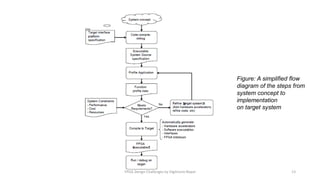
Figure: A simplified flow
diagram of the steps from
system concept to
implementation
on target system
FPGA Design Challenges by Digitronix Nepal 13

FPGA Design Challenges

  • 1.
    Hardware(FPGA) Design Challenges Presentation by DigitronixNepal Web: www.digitronixnepal.com E-Mail: digitronixnepali@gmail.com FPGA Design Challenges by Digitronix Nepal 1
  • 2.
    Contents • FPGA DesignChallenges and Complexity • Addressing Challenges and Complexity • Selecting an FPGA-based prototyping system • FPGA based Design must address • Hardware Software Co-design FPGA Design Challenges by Digitronix Nepal 2
  • 3.
    FPGA design complexityand challenges • Prolonged design cycles with longer design iterations and runtimes because the designs are so large and you may well be pushing the performance envelope • System design complexity (use of DSP blocks, embedded cores and use of IP blocks) • The need to reduce power & part cost • Traditional debug and verification takes too long and fails to provide the required coverage (Synopsys) FPGA Design Challenges by Digitronix Nepal 3
  • 4.
    How can youmost effectively achieve your performance goals in the shortest possible time? • Managing constraints • Faster debug turns and results stability matter • Physical Synthesis • Managing Design Size and Complexity • Addressing Low Power Consumption Demands • Debug in RTL, Not Gates • Debugging and Visibility Enhancement FPGA Design Challenges by Digitronix Nepal 4
  • 5.
    Challenges on FPGA •Design Partitioning: while program don’t fit on single FPGA, program need to be partitioned. • Long bring up : lengthy process on design, test and built a PCB • Difficult to debug: Limitations of internal logic analyzer inside the chip • Performance : affect of impedance matching, multiplexing, clock conversion • Reusability: based upon the FPGA families, however the standard tested program can be customized for different FPGA in short time. (EE Times) FPGA Design Challenges by Digitronix Nepal 5
  • 6.
    Addressing the challenges •Quality PCBs that can accommodate high speeds (e.g., minimal clock skew, equal-length I/Os, stable power and ground, high signal integrity) • Comprehensive self-test capabilities to detect and resolve hardware issues • Integrated logic analyzer support to debug a design partitioned across multiple FPGAs • Partitioning tools that can optimize results • Systems with modular implementations that allow for scalability and reuse. FPGA Design Challenges by Digitronix Nepal 6
  • 7.
    Selecting an FPGA-basedprototyping system Capacity: Without enough gate-level capacity to accommodate your design, you can't build a prototype. Most systems need memory, too, so having sufficient memory available is critical. Scalability: This is the ability to add capacity as needed, including gate-level and memory capacity. Scalability also deals with extensibility -- adding components such as processors and communication interfaces to grow the system functionality. Another dimension of scalability is system replication, the ability to quickly (and cost-effectively) produce copies of a given design for multiple deployments or intersystem testing. Performance: The whole purpose of building an FPGA-based prototype is to achieve sufficient performance for the next level of tasks: hardware verification, software development and optimization, and system test. If your prototype can't deliver the performance, it will fail at its original purpose. Achieving performance requires the PCBs to be specially designed with careful interconnect and I/O design, including load balancing, clock performance, and the use of high-speed communication channels such as gigabit transceivers. FPGA Design Challenges by Digitronix Nepal 7
  • 8.
    Selecting an FPGA-basedprototyping system Compile/partition software: The ability to partition a design reliably across multiple FPGAs is critical to handling large designs. It's very important to have a software tool to make this task easy and reliable. The partitioning software must also optimize I/Os, clocks, and pin multiplexing to ensure maximum performance. Since the partitioning algorithms and hardware architecture are closely related, they yield the best results if they are considered together, so finding an integrated solution for this is preferred. Debug tools: Debugging a design partitioned across multiple FPGAs is all but impossible without a tool that helps set up probes and makes signals easy to track based on their RTL-level names. Debugging should use FPGA I/O efficiently and maintain a useful debug trace depth. Transaction-based interface: A recent DeepChip report stressed the importance of "transactors" -- interfaces that bridge the gap between abstraction levels. This could be a well-known bus protocol such as AXI or an industry-standard transaction protocol such as SCE-MI that communicates between a design mapped to an FPGA and a behavioral simulation. Transactors extend the functionality of the system, allowing it to be used for algorithm/architectural exploration, system integration with virtual prototypes, and exhaustive testing through software-generated corner tests. Where transactors are used, they must be efficient to avoid becoming bottlenecks to overall system performance. FPGA Design Challenges by Digitronix Nepal 8
  • 9.
    Selecting an FPGA-basedprototyping system FPGA Design Challenges by Digitronix Nepal 9
  • 10.
    Selecting an FPGA-basedprototyping system Reliability: A reliable hardware platform is paramount. In order to ensure reliability, a system should have self-test capability and should include protection mechanisms to guard against problems such as overcurrent, overvoltage, and overtemperature. Reusability: The ability to reuse your prototype platform enhances its usefulness, speeds the process of developing new prototypes, and reduces overall costs. Remote management: Managing a prototype remotely makes it easier to deploy for multiple users and projects. As a result, prototype resources can be located anywhere -- in a centralized facility for easy maintenance, for example -- yet used by groups distributed around the world. The ability to download the FPGAs remotely makes it easy to reconfigure a system for any purpose. Whither the state of the art? The state of the art has progressed spectacularly since early forays into FPGA-based prototyping. Commercial systems abound in both size and approach -- from huge emulation boxes costing millions of dollars to modest providers with small, low-end boards. FPGA Design Challenges by Digitronix Nepal 10
  • 11.
    FPGA based designmust address • RTL code analysis, • through embedded design support, functional verification integration, DSP optimization, physical synthesis for early timing • predictability and results stability from one run to the next, incremental features that let you save runtime and preserve working parts of the design, • Integration with FPGA vendors’ P&R systems, debug with visibility enhancement technology, • Power analysis features. FPGA Design Challenges by Digitronix Nepal 11
  • 12.
    Hardware Software CoDesign Figure: Typical embedded computational system: microprocessor, memory, IO FPGA Design Challenges by Digitronix Nepal 12
  • 13.
    Figure: A simplifiedflow diagram of the steps from system concept to implementation on target system FPGA Design Challenges by Digitronix Nepal 13