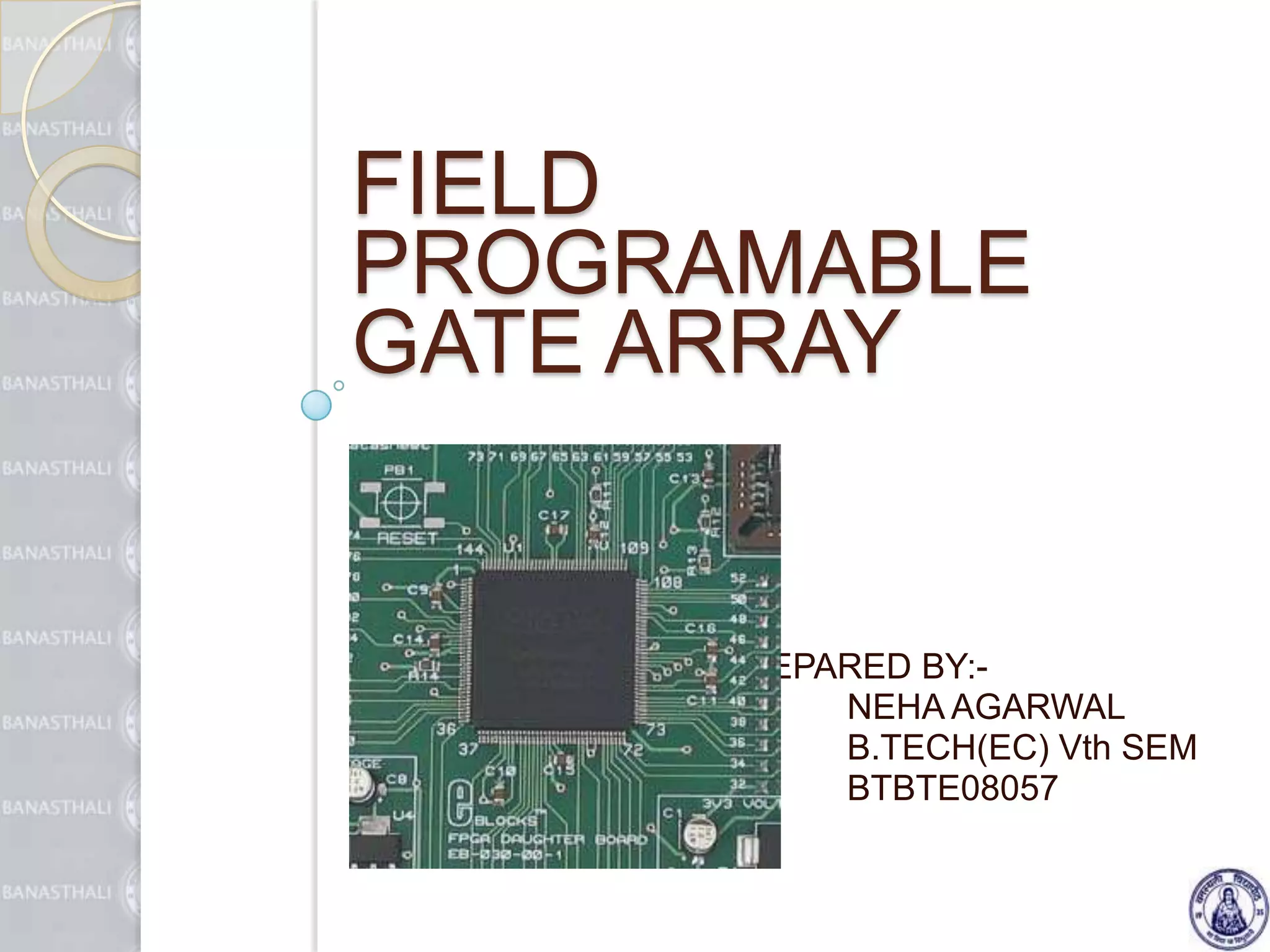
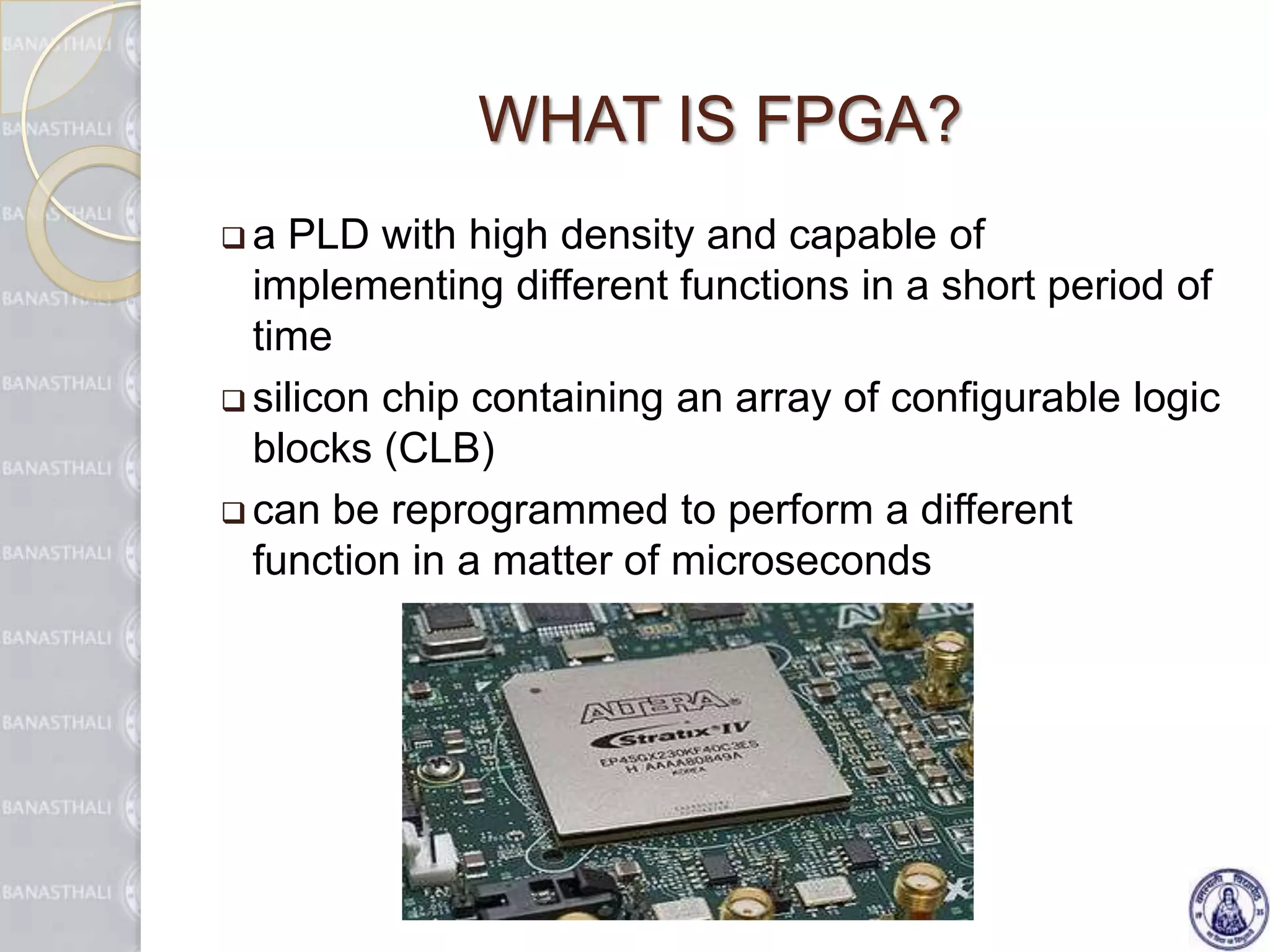
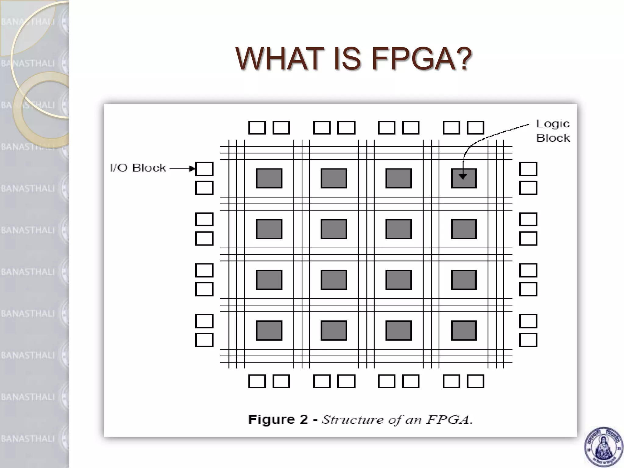
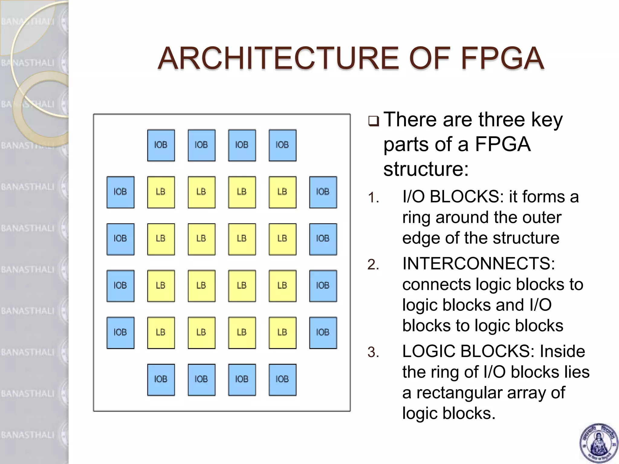
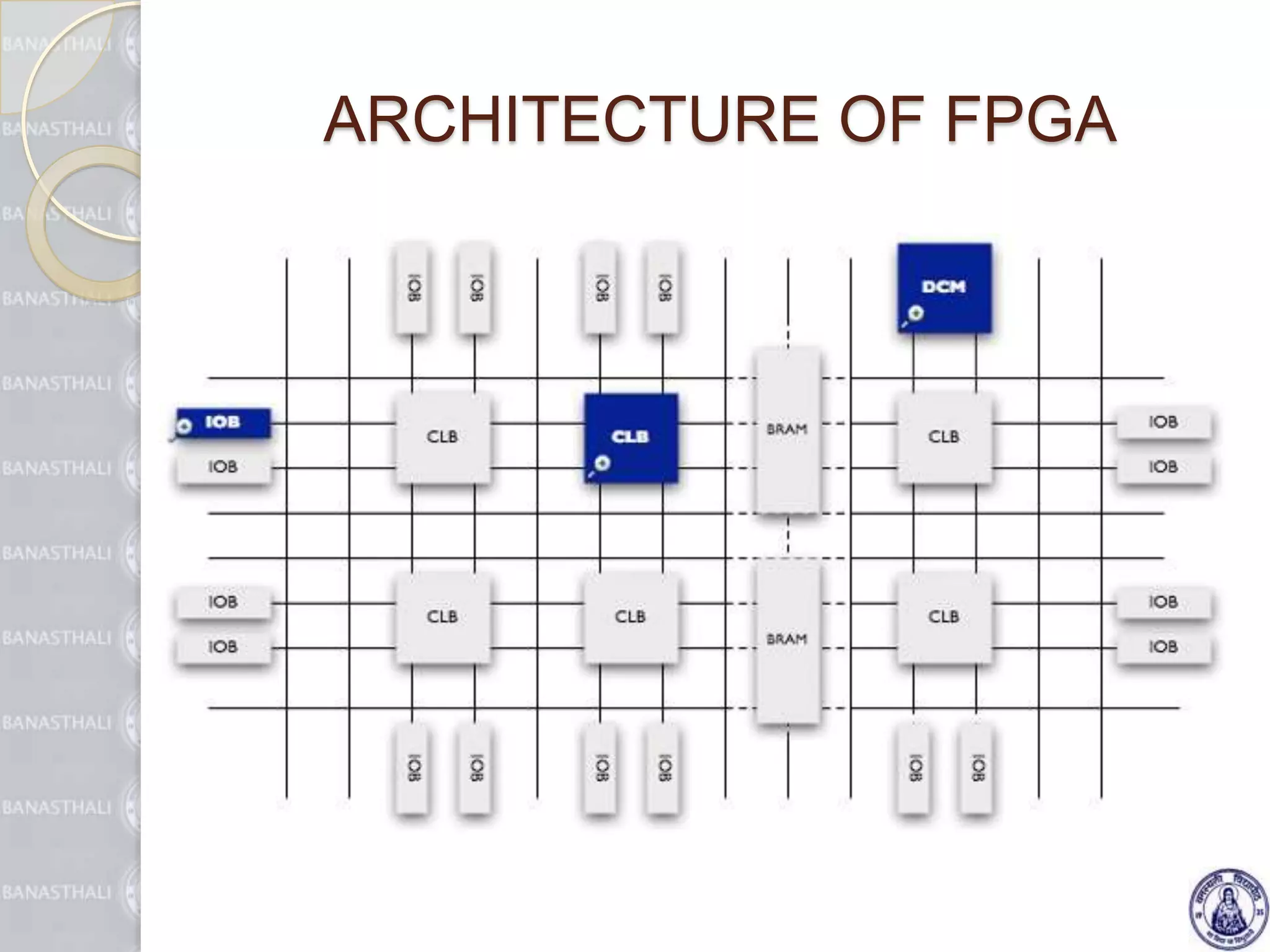
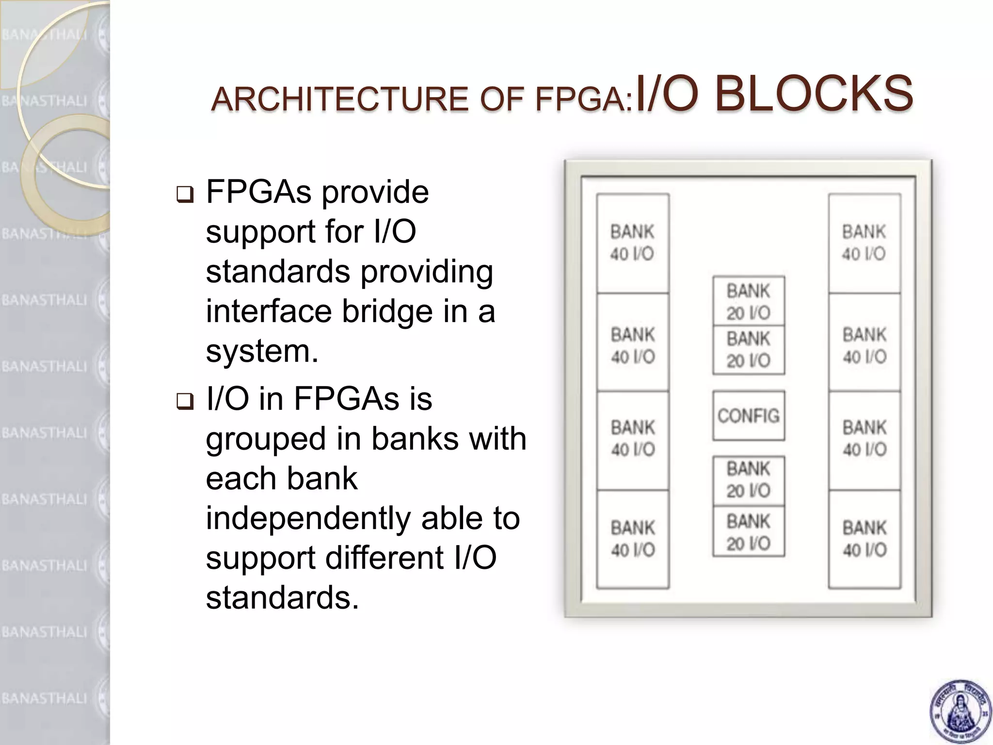
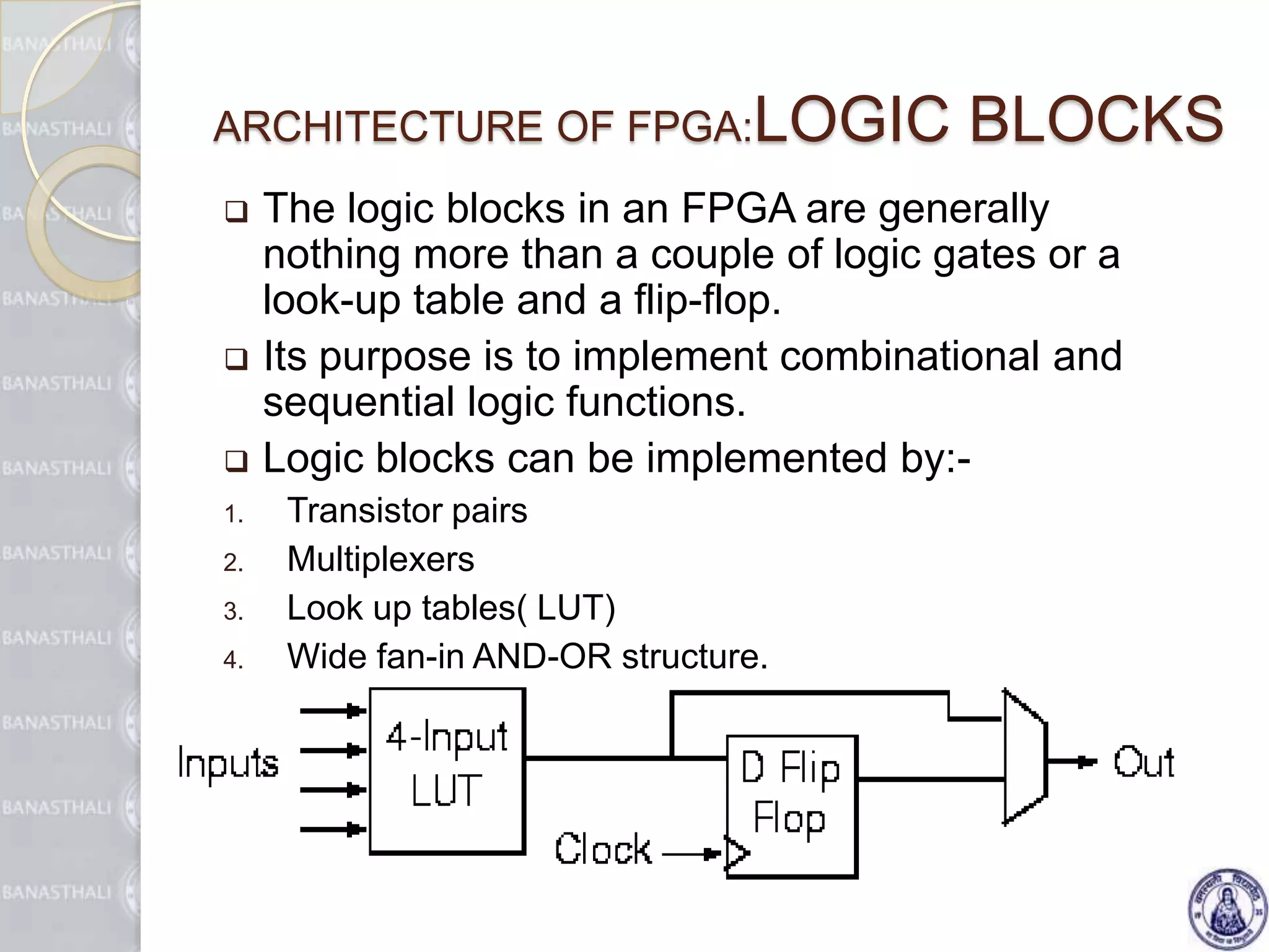
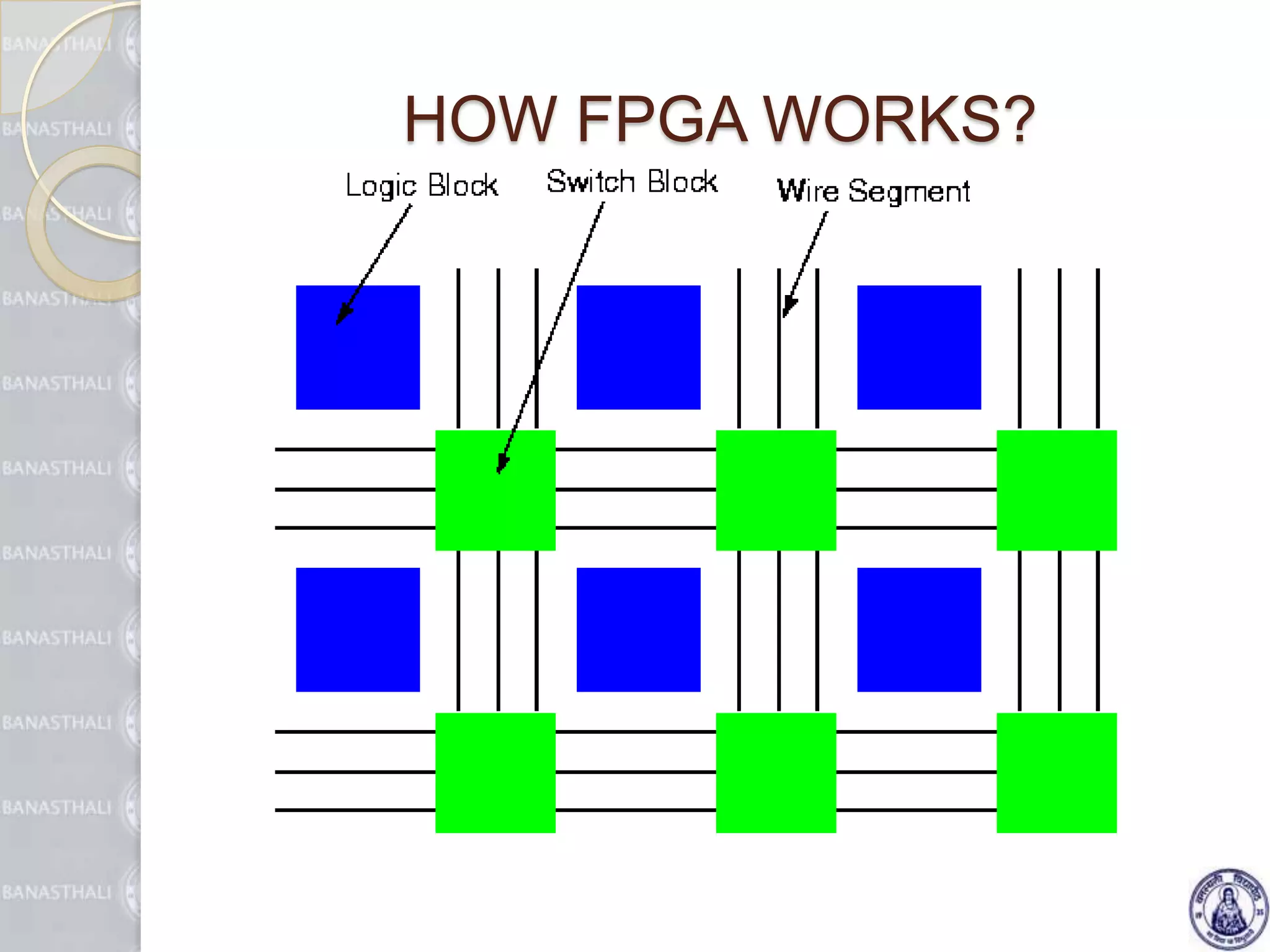
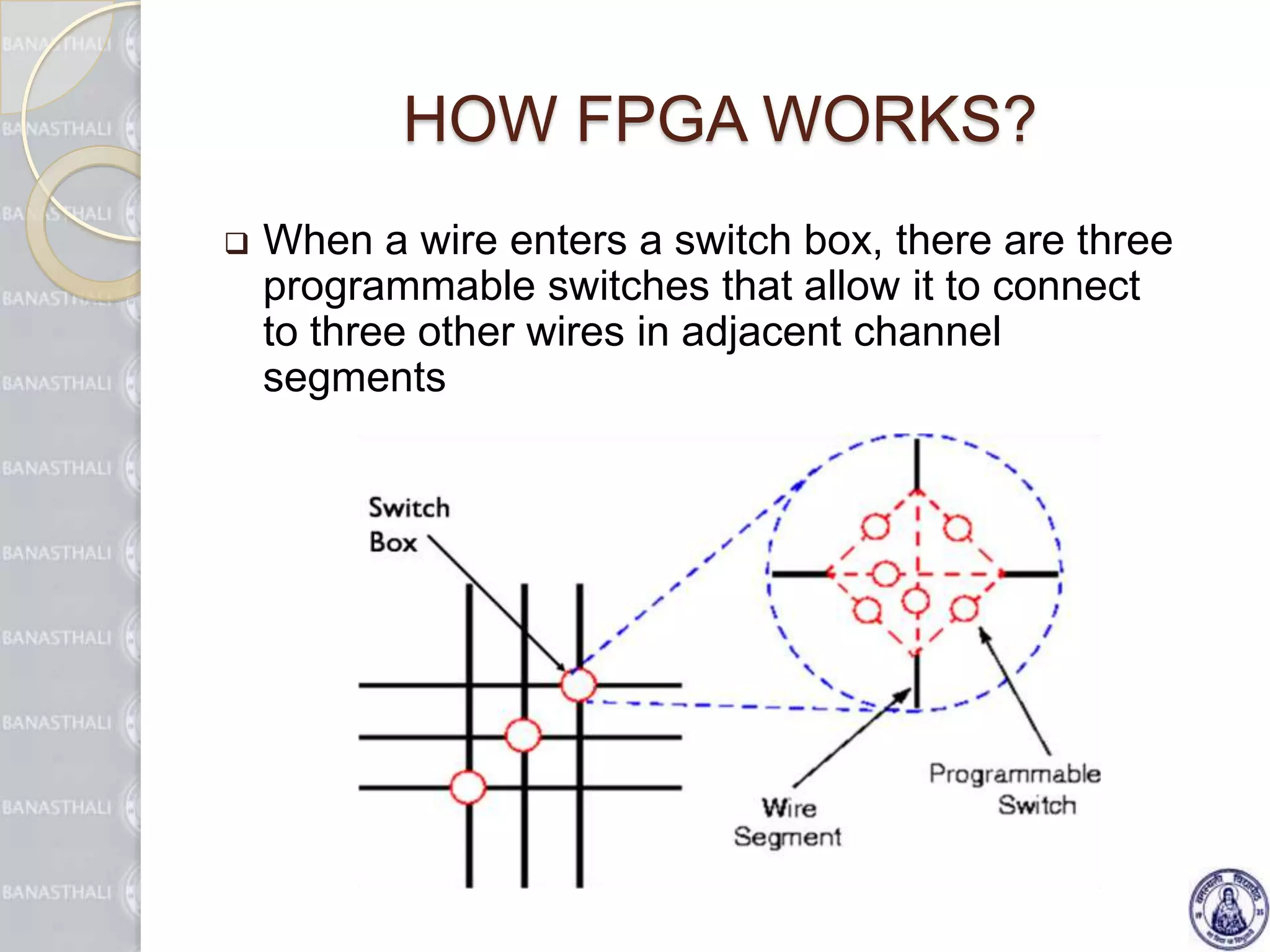
FIELD PROGRAMABLE GATE ARRAYPREPARED BY:-		NEHA AGARWAL	B.TECH(EC) Vth SEM	BTBTE08057
WHAT IS FPGA?a PLD with high density and capable of implementing different functions in a short period of time
silicon chip containing an array of configurable logic blocks (CLB)
can be reprogrammed to perform a different function in a matter of microsecondsWHAT IS FPGA?
WHAT IS PROGRAMMABLE LOGIC DEVICE (PLD)?is an electronic component used to build reconfigurable digital circuits
has an undefined function at the time of manufacture
before using in a circuit it must be programmed or reconfigured
can be customized as per needs of the user by programming
can be reprogrammed in case of problemsARCHITECTURE OF FPGAThere are three key parts of a FPGA structure: I/O BLOCKS: it forms a ring around the outer edge of the structureINTERCONNECTS: connects logic blocks to logic blocks and I/O blocks to logic blocksLOGIC BLOCKS: Inside the ring of I/O blocks lies a rectangular array of logic blocks.
ARCHITECTURE OF FPGA
ARCHITECTURE OF FPGA:I/O BLOCKSFPGAs provide support for I/O standards providing interface bridge in a system.
I/O in FPGAs is grouped in banks with each bank independently able to support different I/O standards.ARCHITECTURE OF FPGA:LOGIC BLOCKSThe logic blocks in an FPGA are generally nothing more than a couple of logic gates or a look-up table and a flip-flop.
Its purpose is to implement combinational and sequential logic functions.
Logic blocks can be implemented by:-Transistor pairsMultiplexers Look up tables( LUT)Wide fan-in AND-OR structure.
ARCHITECTURE OF FPGA: ROUTING MATRIXAn FPGA device contains flexible programmable routing matrix which is used to connect logic blocks with each other.
There are various type of connection lines in FPGA:long lines are used to connect distant logic blocksshort lines connect neighboring blocks with each otherdedicated clock trees are used to distribute synchronization signalsdedicated set/reset lines are used to reset all flip-flops in the FPGA
HOW FPGA WORKS?
HOW FPGA WORKS?When a wire enters a switch box, there are three programmable switches that allow it to connect to three other wires in adjacent channel segmentsPROGRAMMING A FPGAUnderstand and define design requirements
Design description
Behavioral simulation
Synthesis

Field programable gate array