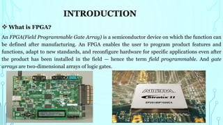
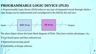
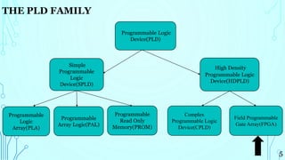
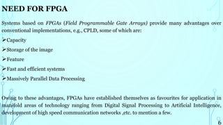
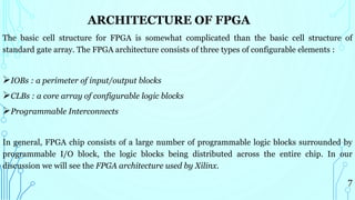
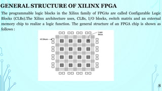
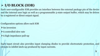
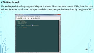
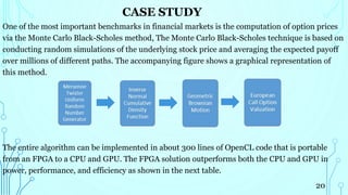
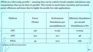
This document summarizes a seminar presentation on field programmable gate arrays (FPGAs) given by Saransh Choudhary. The presentation covered the introduction, architecture, applications and conclusion of FPGAs. It discussed the components of an FPGA including configurable logic blocks, input/output blocks and programmable interconnects. A case study demonstrated how FPGAs can efficiently implement Monte Carlo option pricing simulations. Applications mentioned included digital signal processing, image processing, radar systems and supercomputers.

![EXAMPLE : THREE-BAND AUDIO EQUALIZER
In the brief example below, a three-band audio equalizer has been implemented on an FPGA. For
reasons of clarity, we use half-band filters in the equalizer algorithm. In this, a digital high-pass
(HP) and a digital low-pass (LP) each split the discrete-time input signal into two sub-bands. In
turn, the sum of the two sub-bands yields the input signal.
In MATLAB, it is possible to calculate this type of filter using just a few instructions:
% Buttworth low-pass filter with cut-off frequency w1:
[G_LP_num, G_LP_den] = butter(2, w1);
% Complement-res high-pass filter:
G_HP_num = G_LP_den - G_LP_num;
G_HP_den = G_LP_den;
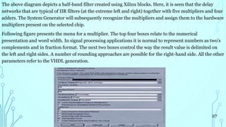
The block diagram for the entire equalizer with two half-band filter stages is shown.
23](https://image.slidesharecdn.com/seminaronfieldprogrammablegatearrays-170911111456/85/Seminar-on-field-programmable-gate-array-23-320.jpg)
![Fig. : Block diagram of Three-band digital equalizer
Each of the three bands is multiplied by a coefficient (K_Low, K_Mid and K_High). The output
signal y[.] is given by the sum of the three weighted sub-bands. If one of the coefficients is greater
than one then the corresponding band is amplified. If it is less than one, then the band is
attenuated.
24](https://image.slidesharecdn.com/seminaronfieldprogrammablegatearrays-170911111456/85/Seminar-on-field-programmable-gate-array-24-320.jpg)