Download as PDF, PPTX
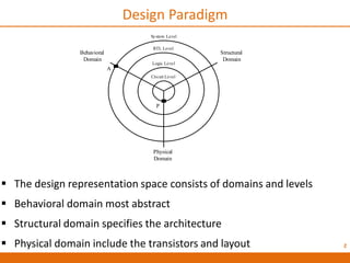
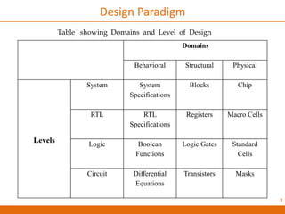
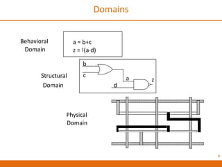
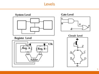
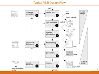
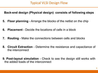
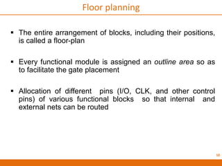
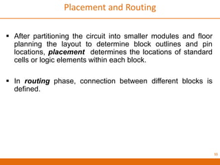


The VLSI design flow consists of three domains - behavioral, structural, and physical - and multiple levels from system to circuit level. The front-end design includes logic synthesis to generate a netlist from HDL code through technology mapping and optimization. Back-end physical design involves floorplanning, placement of cells, routing of interconnects, and simulation to verify functionality and timing.