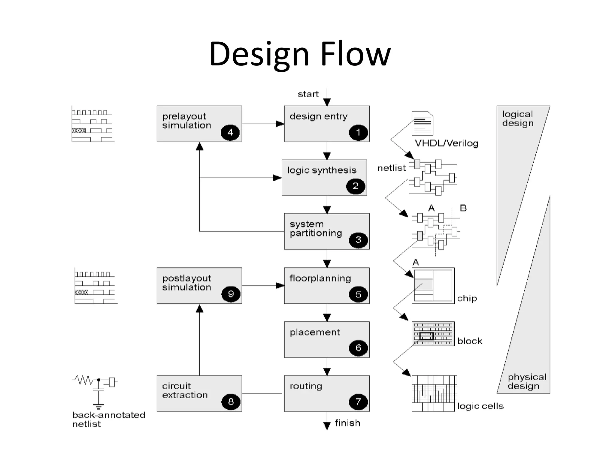
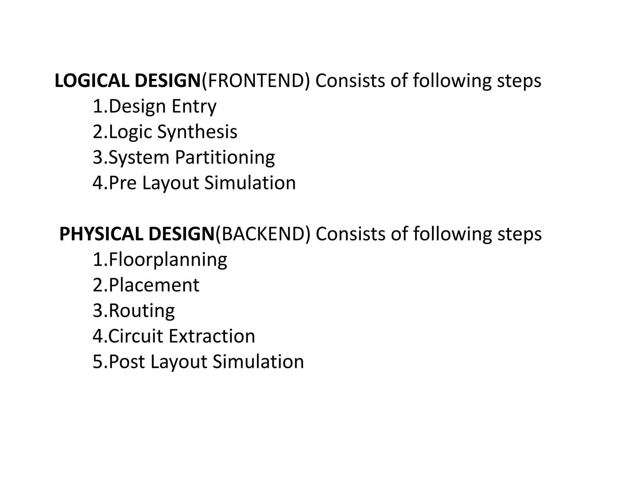
The document describes the ASIC design flow, which consists of two main phases: logical design (frontend) and physical design (backend).
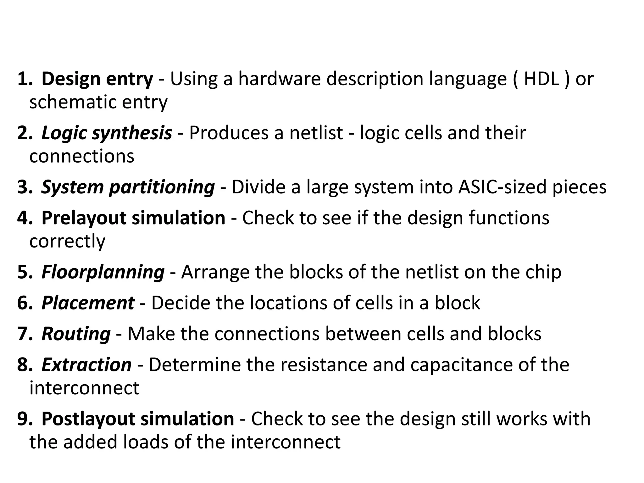
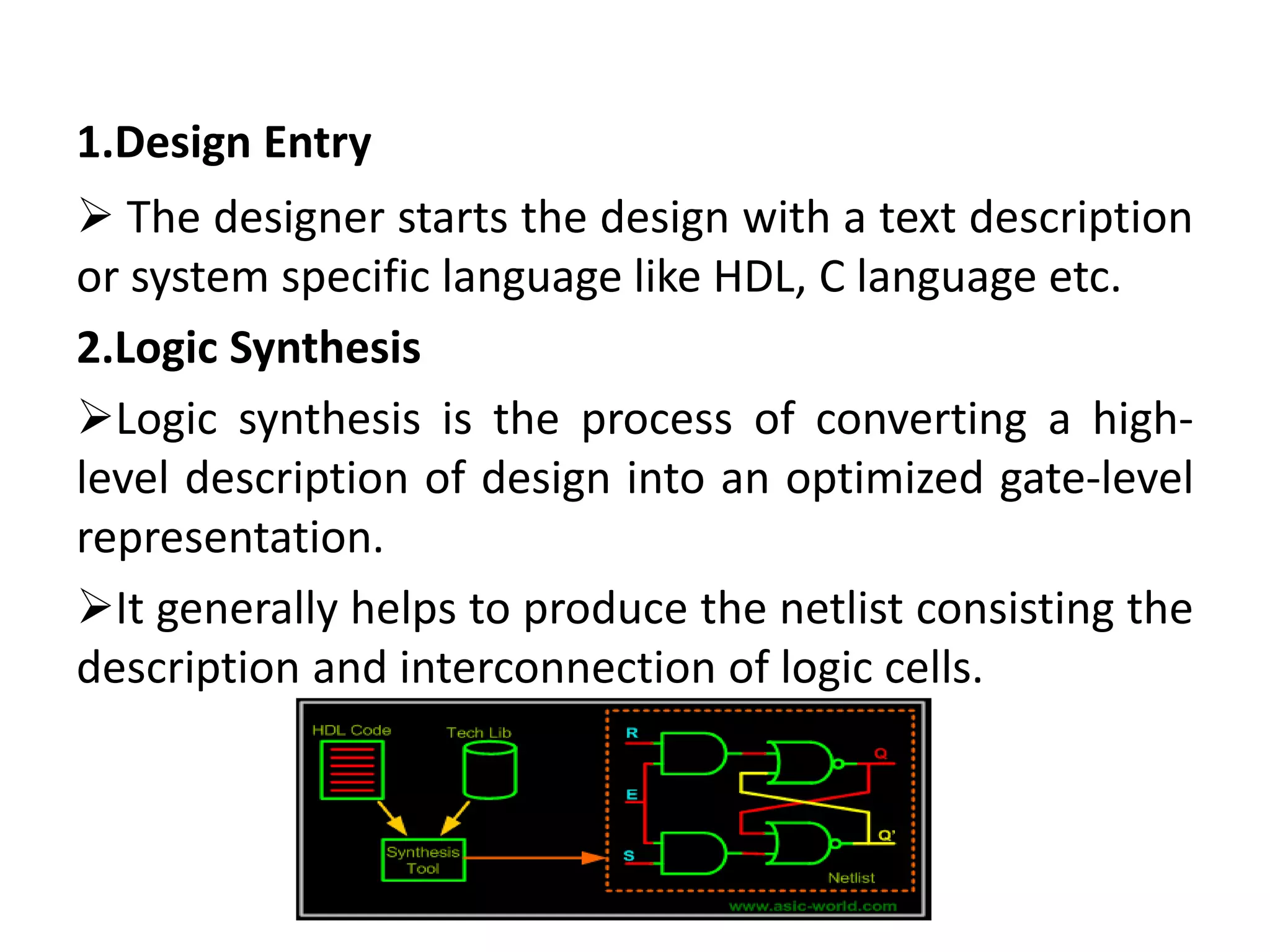
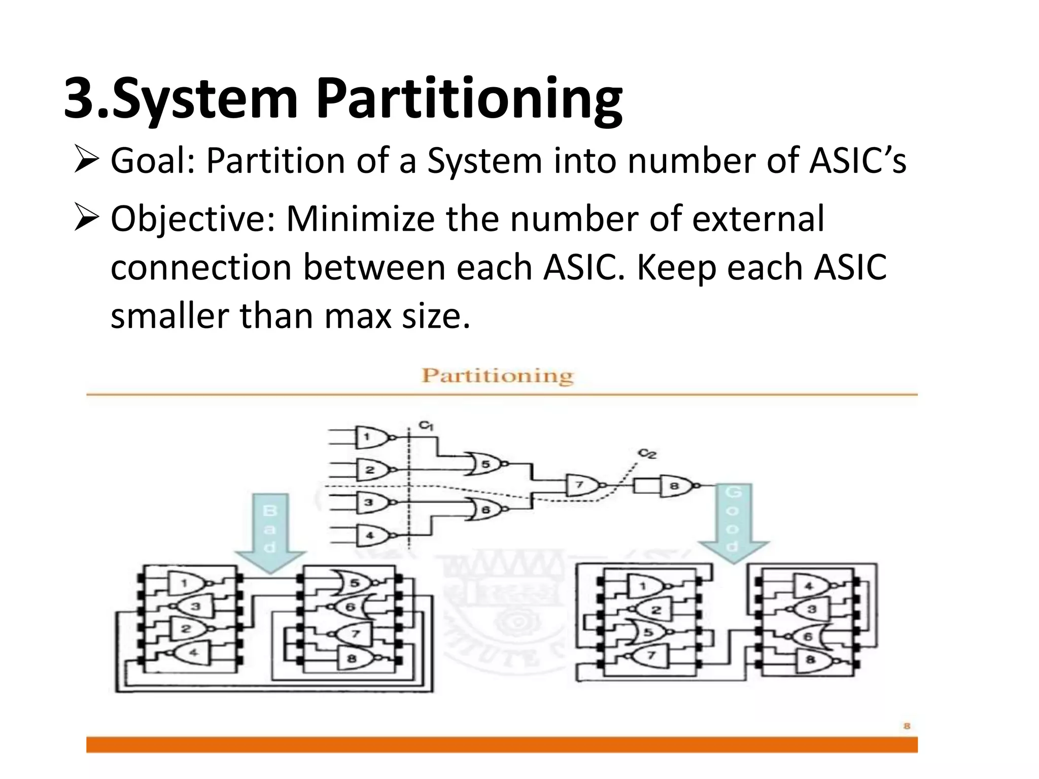
The logical design phase includes design entry, logic synthesis, system partitioning, and pre-layout simulation. This phase converts the design from HDL or schematic to a netlist.
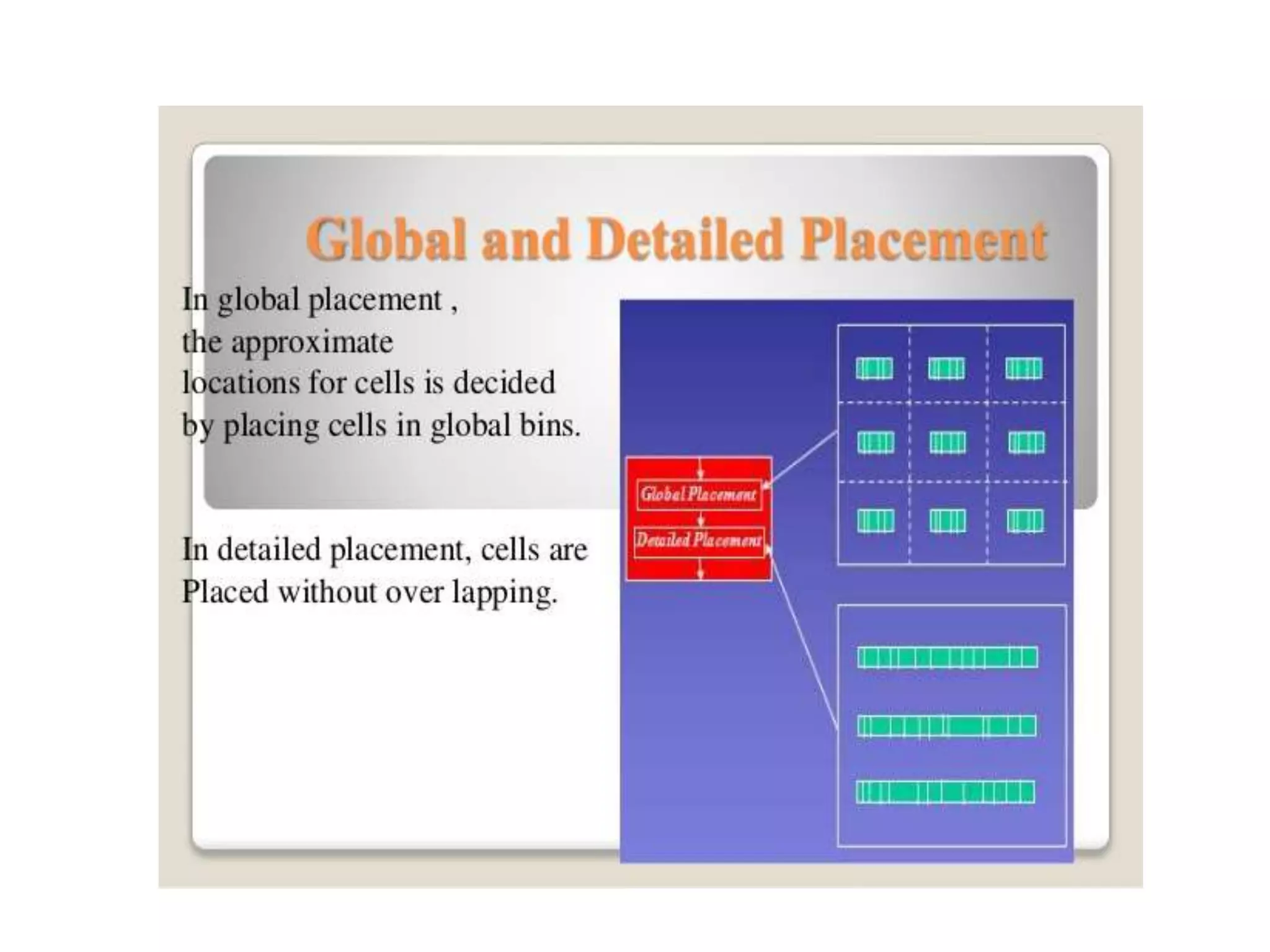
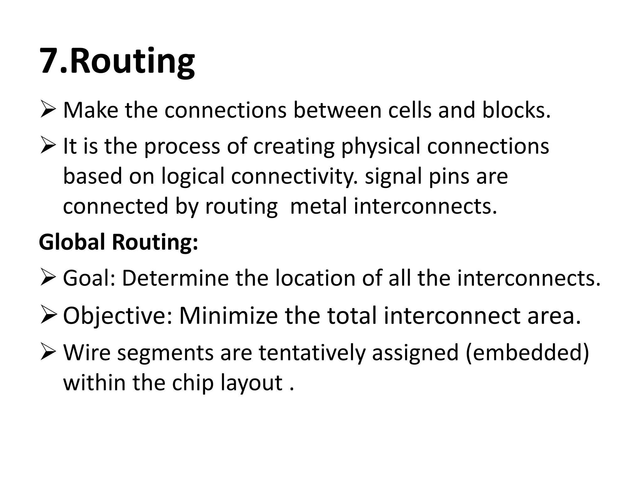
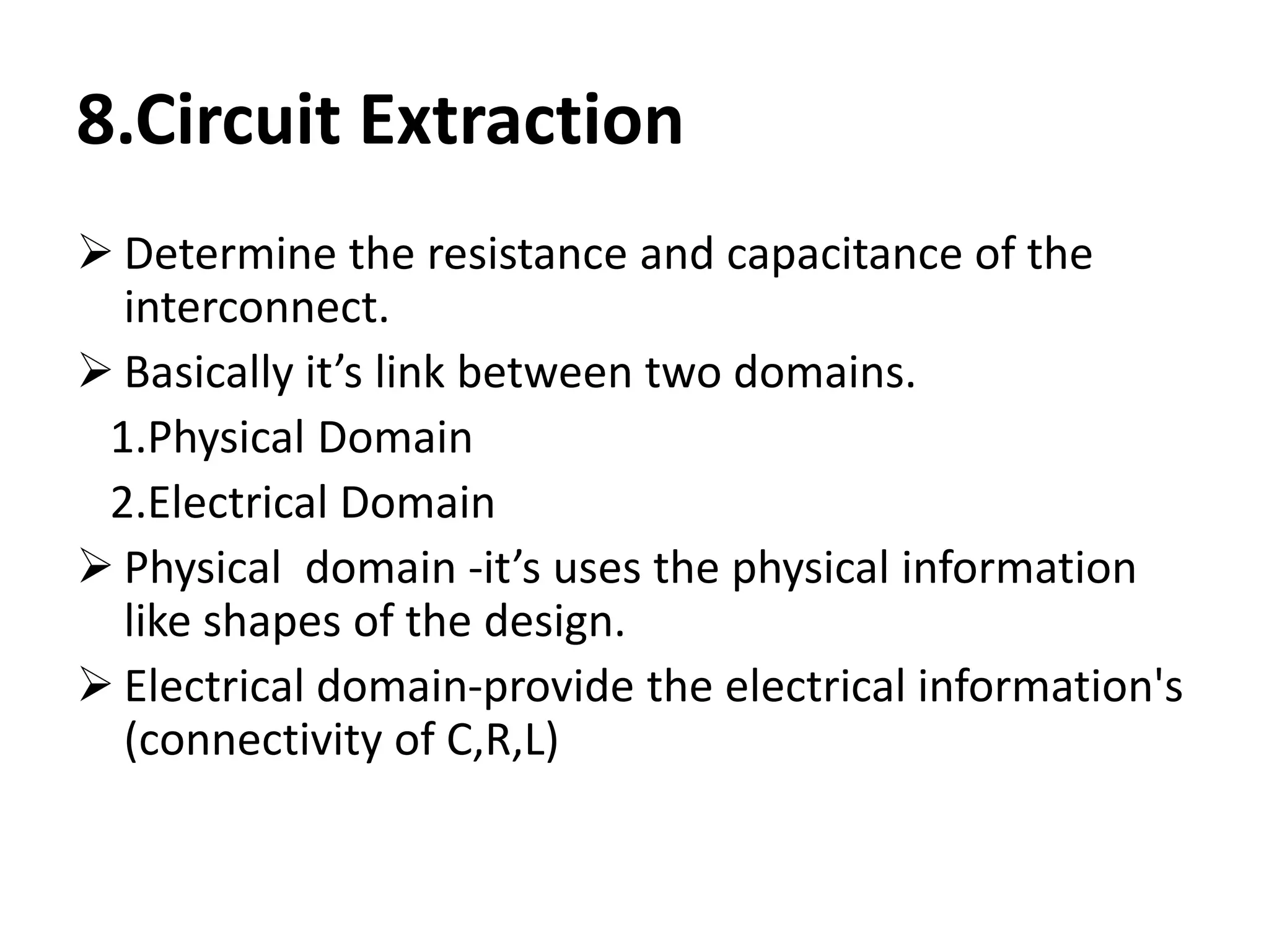
The physical design phase includes floorplanning, placement, routing, circuit extraction, and post-layout simulation. This phase adds physical details and checks timing with parasitics. Floorplanning places blocks, placement assigns cell locations, and routing connects cells and blocks. Circuit extraction determines resistances and capacitances, and post-layout simulation verifies functionality and timing.