Download to read offline
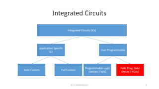
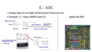
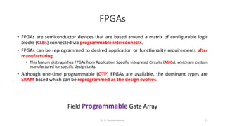
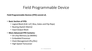
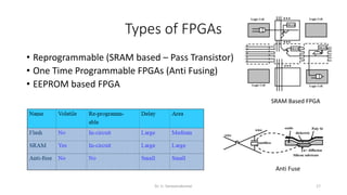
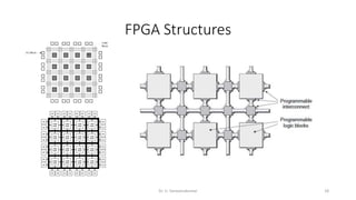
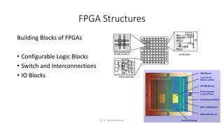
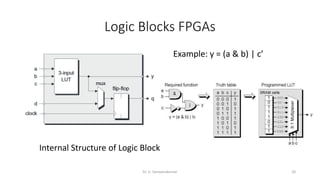
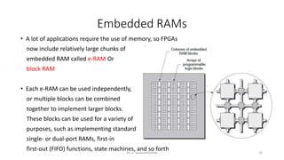
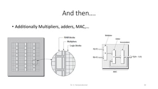
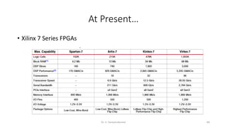


Field Programmable Gate Arrays (FPGAs) are semiconductor devices that contain programmable logic components and programmable interconnects. FPGAs can be reprogrammed to desired functionality requirements after manufacturing. The document discusses the building blocks of FPGAs, including configurable logic blocks (CLBs), interconnects, input/output blocks, block RAM, digital signal processing slices, and clock management resources. It also covers FPGA routing architectures and common FPGA design flows.