Download as PPSX, PPTX
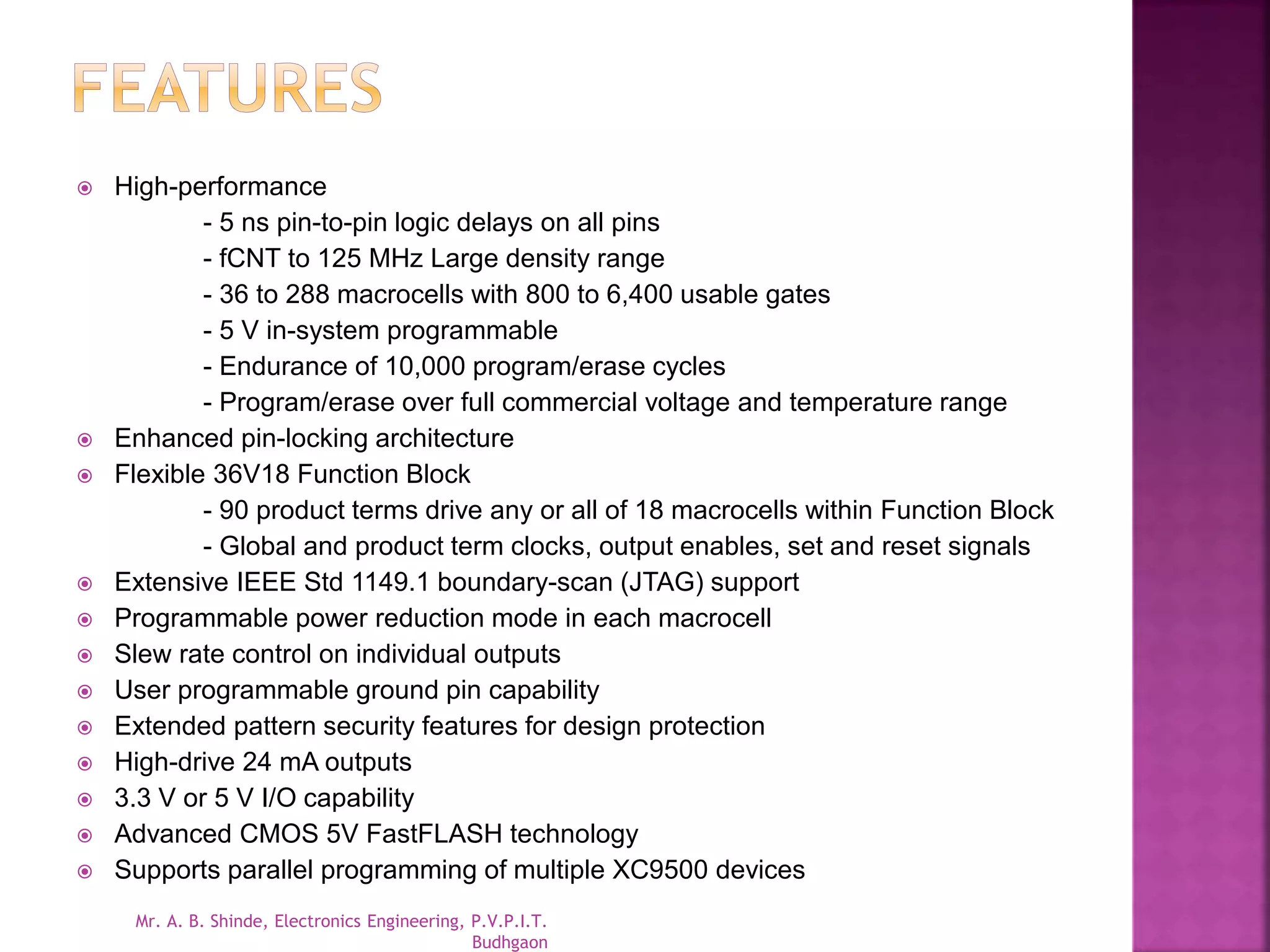
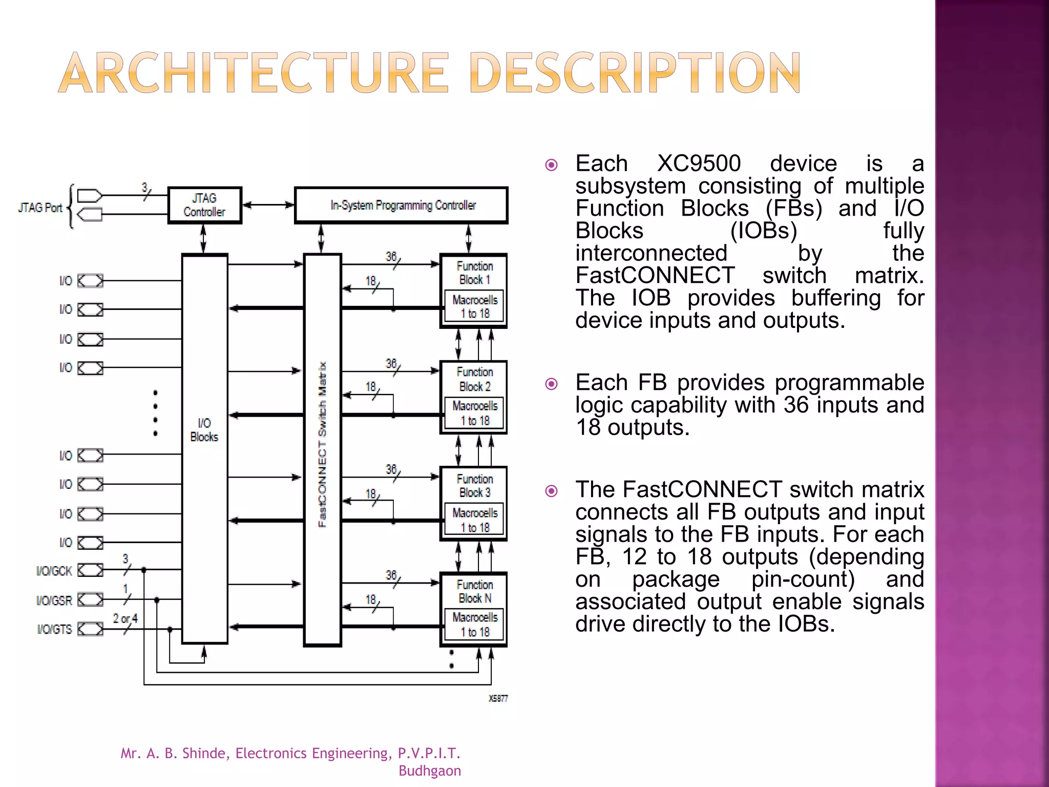
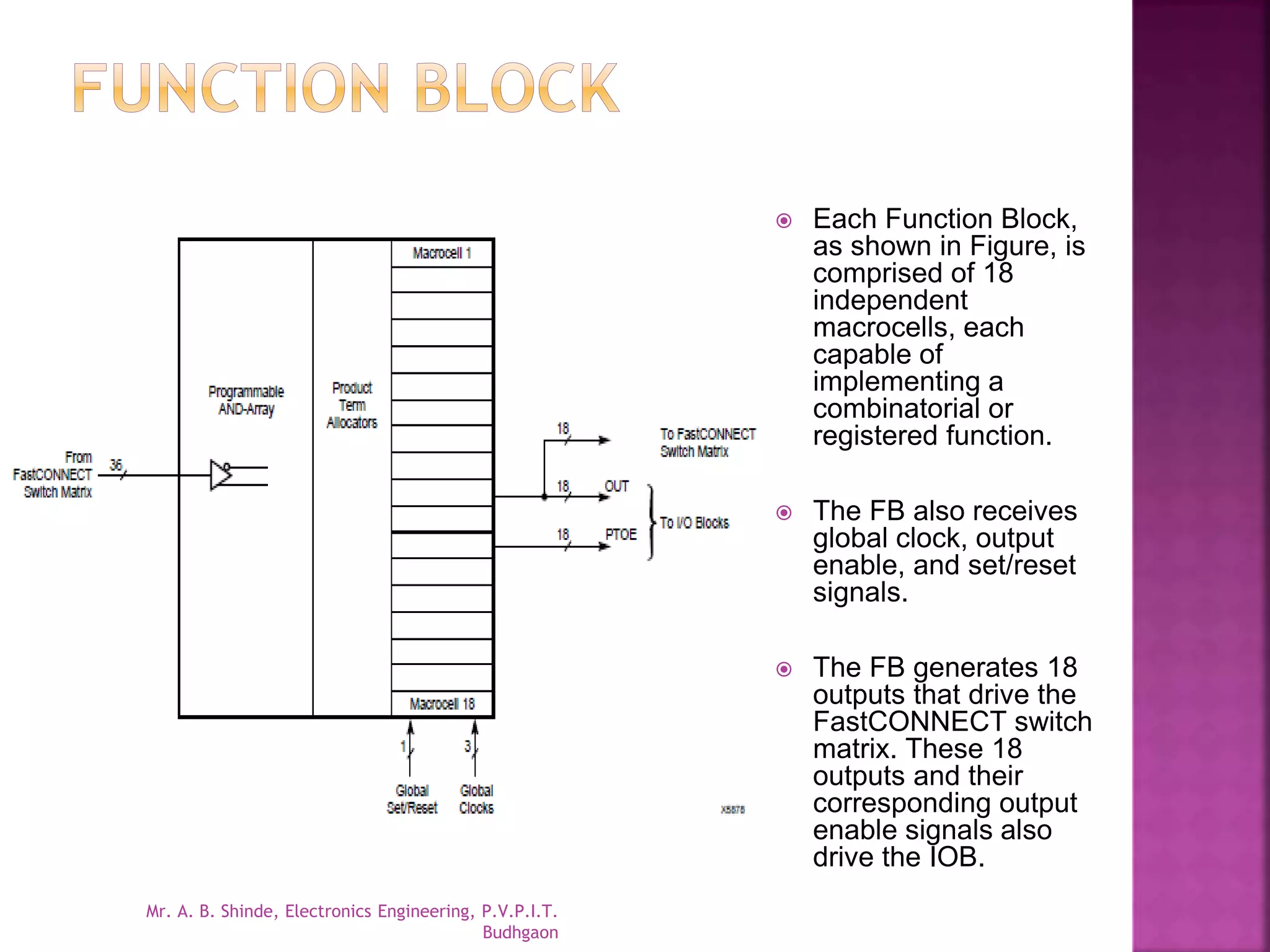
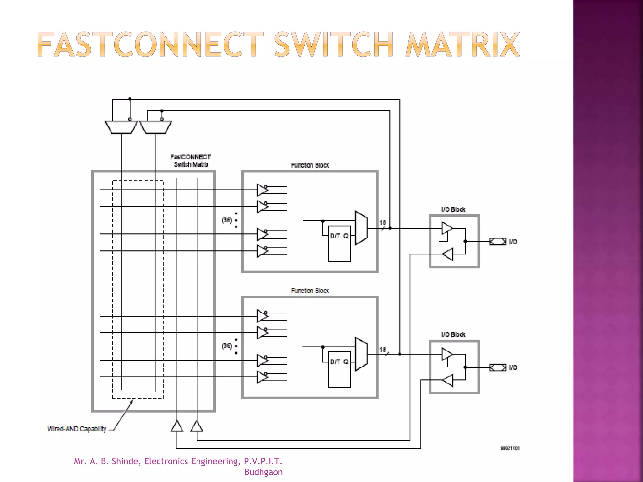

1) The document describes the architecture and features of the XC9500 CPLD, which consists of multiple Function Blocks and I/O Blocks interconnected by a FastCONNECT switch matrix. 2) Each Function Block provides programmable logic with 36 inputs and 18 outputs, and contains 18 independent macrocells that can each implement combinatorial or registered logic functions. 3) The I/O Block interfaces between internal logic and user I/O pins, and contains input/output buffers and output enable selection multiplexers.
Mr. A. B. Shinde is presented as an assistant professor in Electronics Engineering at P.V.P.I.T., Budhgaon.
Illustrates XC9500 device architecture with Function Blocks (FBs) and I/O Blocks (IOBs) interconnected via FastCONNECT, highlighting programmable logic capabilities.
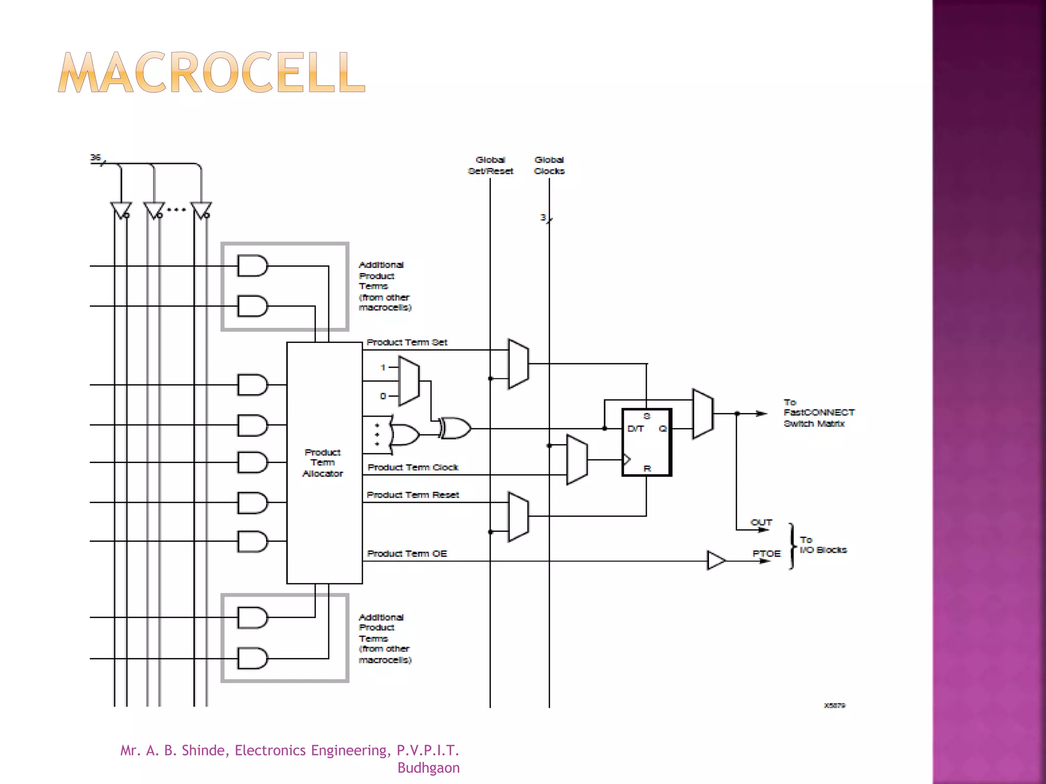
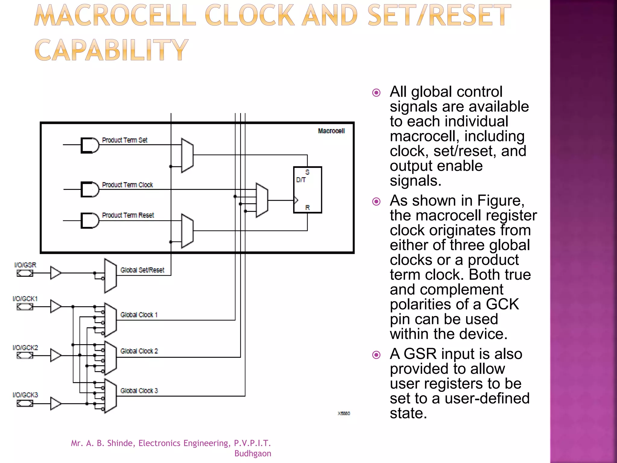
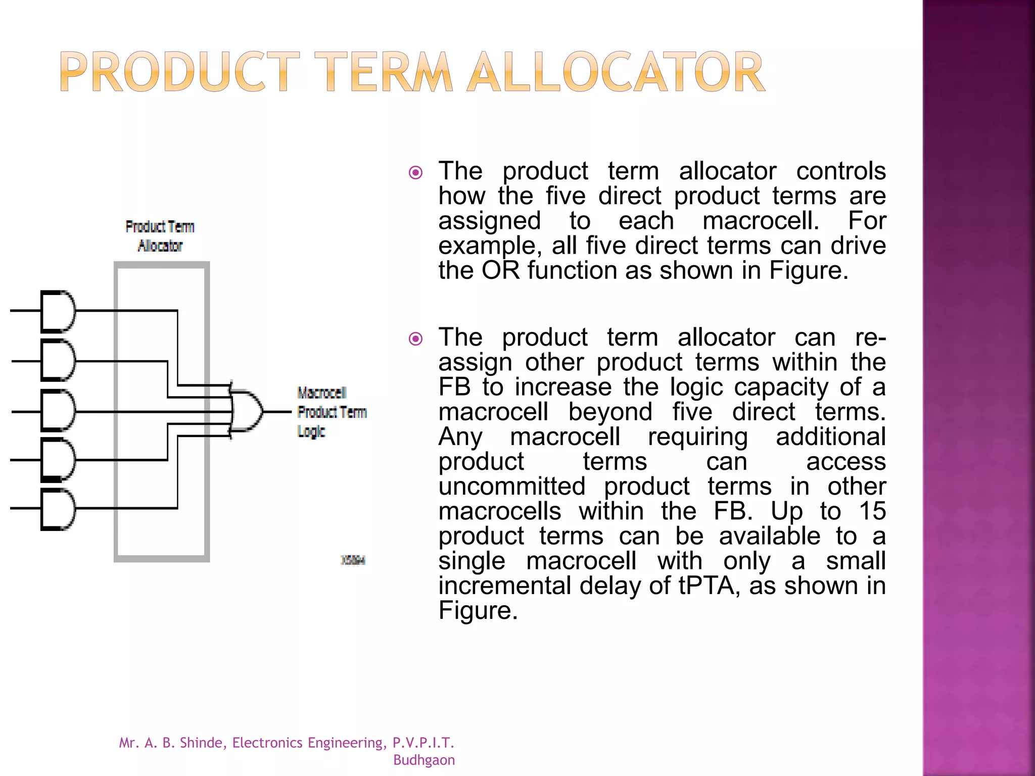
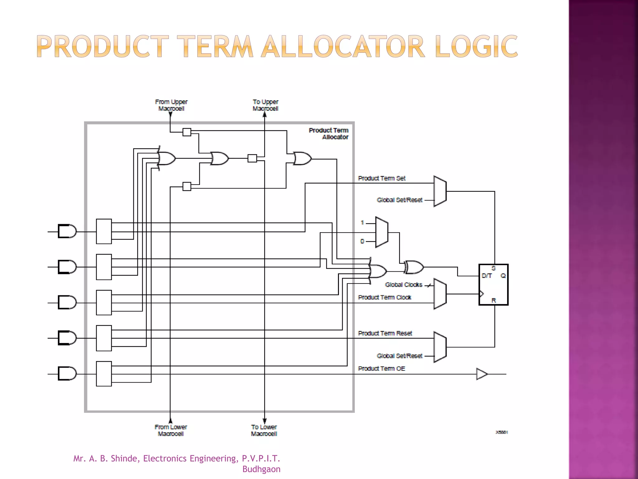
Explains the configuration and logic implementation within Function Blocks, including product term allocation and macrocell control signals.
Explains the configuration and logic implementation within Function Blocks, including product term allocation and macrocell control signals.
Details the FastCONNECT switch matrix capabilities, allowing multiple internal connections and enhancing logic without additional timing delays.
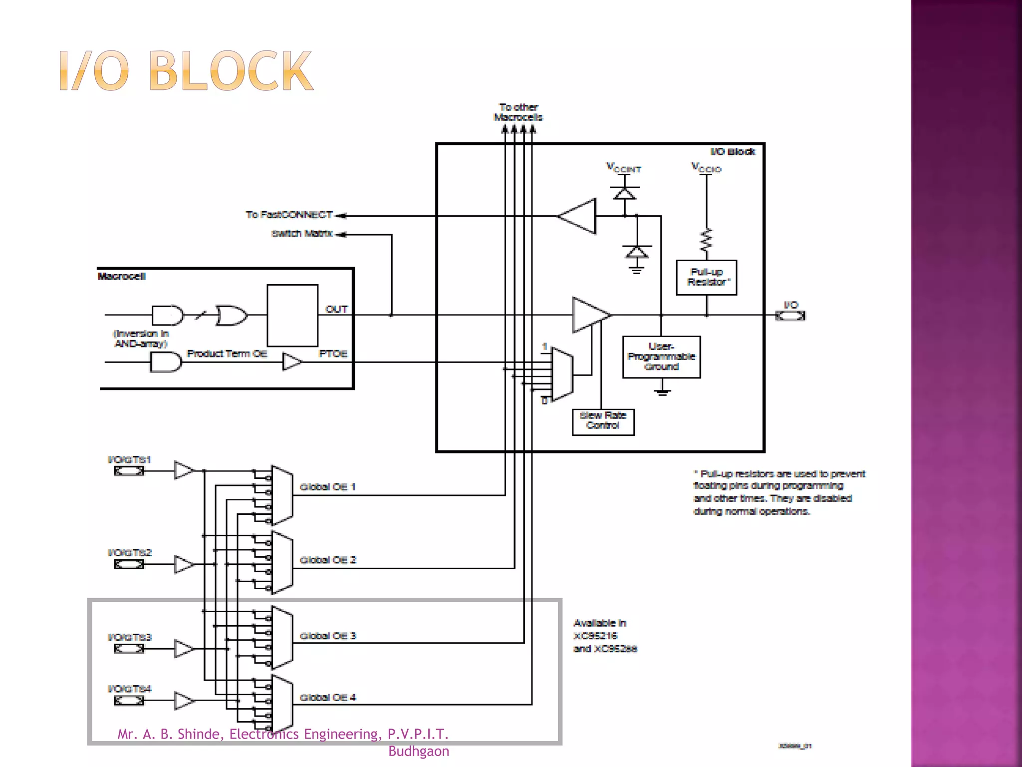
Describes the function of the I/O Block (IOB) with respect to user I/O pins, including buffer compatibility and output control features.
Provides contact details for Mr. A. B. Shinde for further communications as part of the presentation's conclusion.