This presentation gives an overview of FPGA devices. An FPGA is a device that contains a matrix of re-configurable gate array logic circuitry. When a FPGA is configured, the internal circuitry is connected in a way that creates a hardware implementation of the software application.
FPGA devices can deliver the performance and reliability of dedicated hardware circuitry.
An application-specific IC (ASIC) can be either a digital or an analog circuit. As their name implies, ASICs are not reconfigurable; they perform only one specific function. For example, a speed controller IC for a remote control car is hard-wired to do one job and could never become a microprocessor. An ASIC does not contain any ability to follow alternate instructions.
FPGA are a special form of Programmable logic devices(PLDs) with higher densities as compared to custom ICs and capable of implementing functionality in a short period of time using computer aided design (CAD) software....by mathewsubin3388@gmail.com
Routing in Integrated circuits is an important task which requires extreme care while placing the modules and circuits and connecting them with each other.
TYPES OF PLACEMENT,GOOD PLACEMENT VS. BAD PLACEMENT ,ALGORITHMS, ASIC DESIGN FLOW DIAGRAM,DEFINITION OF PLACEMENT,TECHNIQUES USED FOR PLACEMENT,PLACEMENT TRENDS,SOLUTIONS
This presentation discusses the basics of Pass Transistor Logic, its advantages, limitation and finally implementation of Boolean functions/Combinational Logic circuits using Pass Transistor Logic.
Field-programmable gate array\
only for these students that are intrested in Field-programmable gate array
field-programmable gate array (FPGA) is an integrated circuit designed to be configured by a customer or a designer after manufacturing – hence "field-programmable". The FPGA configuration is generally specified using a hardware description language (HDL), similar to that used for an application-specific integrated circuit (ASIC). (Circuit diagrams were previously used to specify the configuration, as they were for ASICs
The FPGA industry sprouted from programmable read-only memory (PROM) and programmable logic devices (PLDs). PROMs and PLDs both had the option of being programmed in batches in a factory or in the field (field-programmable). However, programmable logic was hard-wired between logic gates.[6]
In the late 1980s, the Naval Surface Warfare Center funded an experiment proposed by Steve Casselman to develop a computer that would implement 600,000 reprogrammable gates. Casselman was successful and a patent related to the system was issued in 1992.[6]
Some of the industry's foundational concepts and technologies for programmable logic arrays, gates, and logic blocks are founded in patents awarded to David W. Page and LuVerne R. Peterson in 1985.
A low power cmos analog circuit design for acquiring multichannel eeg signalsVLSICS Design
EEG signals are the signatures of neural activities and are captured by multiple-electrodes and the signals are recorded from pairs of electrodes. To acquire these multichannel signals a low power CMOS circuit was designed and implemented. The design operates in weak inversion region employing sub threshold
source coupled logic. A 16 channel differential multiplexer is designed by utilizing a transmission gate with
dynamic threshold logic and a 4 to 16 decoder is used to select the individual channels. The ON and OFF
resistance of the transmission gate obtained is 27 ohms and 10 M ohms respectively. The power dissipation
achieved is around 337nW for a dynamic range of 1μV to 0.4 V.
Presentation on various logic families like RTL, DTL, TTL, IIL etc with diagram, advantages and limitations plus some basic concepts like fan out, noise margin, propagation delay.
Design and Implementation of Submicron Level 10T Full Adder in ALU Using Cell...IJERA Editor
As technology scales into the nanometer regime leakage current, active power, delay and area are becoming important metric for the analysis and design of complex circuits. The main concern in mobile and battery based systems are leakage current and power dissipation. A transistor resizing approach for 10 transistor single bit full adder cells is used to determine optimal sleep transistor size which reduces power dissipation and leakage current. A submicron level 10-transistor single bit full adder cell is considered to achieve low leakage current, reduced power dissipation and high speed. In this paper initially 10T full adder cell is designed with submicron technique and later this is employed to design an ALU adder unit. The modified ALU is simulated and synthesized successfully on cadence 180nm technology.
AREA EFFICIENT 3.3GHZ PHASE LOCKED LOOP WITH FOUR MULTIPLE OUTPUT USING 45NM ...VLSICS Design
This paper present area efficient layout designs for 3.3GigaHertz (GHz) Phase Locked loop (PLL) with four multiple output. Effort has been taken to design Low Power Phase locked loop with multiple output, using VLSI technology. VLSI Technology includes process design, trends, chip fabrication, real circuit parameters, circuit design, electrical characteristics, configuration building blocks, switching circuitry, translation onto silicon, CAD and practical experience in layout design. The proposed PLL is designed using 45 nm CMOS/VLSI technology with microwind 3.1. This software allows designing and simulating an integrated circuit at physical description level. The main novelties related to the 45 nm technology are the high-k gate oxide, metal gate and very low-k interconnect dielectric. The effective gate length required for 45 nm technology is 25nm. Low Power (0.211miliwatt) phase locked loop with four multiple outputs as PLL8x, PLL4x, PLL2x, & PLL1x of 3.3 GHz, 1.65 GHz, 0.825 GHz, and 0.412 GHz respectively is obtained using 45 nm VLSI technology.
NO1 Uk best vashikaran specialist in delhi vashikaran baba near me online vas...Amil Baba Dawood bangali
Contact with Dawood Bhai Just call on +92322-6382012 and we'll help you. We'll solve all your problems within 12 to 24 hours and with 101% guarantee and with astrology systematic. If you want to take any personal or professional advice then also you can call us on +92322-6382012 , ONLINE LOVE PROBLEM & Other all types of Daily Life Problem's.Then CALL or WHATSAPP us on +92322-6382012 and Get all these problems solutions here by Amil Baba DAWOOD BANGALI
#vashikaranspecialist #astrologer #palmistry #amliyaat #taweez #manpasandshadi #horoscope #spiritual #lovelife #lovespell #marriagespell#aamilbabainpakistan #amilbabainkarachi #powerfullblackmagicspell #kalajadumantarspecialist #realamilbaba #AmilbabainPakistan #astrologerincanada #astrologerindubai #lovespellsmaster #kalajaduspecialist #lovespellsthatwork #aamilbabainlahore#blackmagicformarriage #aamilbaba #kalajadu #kalailam #taweez #wazifaexpert #jadumantar #vashikaranspecialist #astrologer #palmistry #amliyaat #taweez #manpasandshadi #horoscope #spiritual #lovelife #lovespell #marriagespell#aamilbabainpakistan #amilbabainkarachi #powerfullblackmagicspell #kalajadumantarspecialist #realamilbaba #AmilbabainPakistan #astrologerincanada #astrologerindubai #lovespellsmaster #kalajaduspecialist #lovespellsthatwork #aamilbabainlahore #blackmagicforlove #blackmagicformarriage #aamilbaba #kalajadu #kalailam #taweez #wazifaexpert #jadumantar #vashikaranspecialist #astrologer #palmistry #amliyaat #taweez #manpasandshadi #horoscope #spiritual #lovelife #lovespell #marriagespell#aamilbabainpakistan #amilbabainkarachi #powerfullblackmagicspell #kalajadumantarspecialist #realamilbaba #AmilbabainPakistan #astrologerincanada #astrologerindubai #lovespellsmaster #kalajaduspecialist #lovespellsthatwork #aamilbabainlahore #Amilbabainuk #amilbabainspain #amilbabaindubai #Amilbabainnorway #amilbabainkrachi #amilbabainlahore #amilbabaingujranwalan #amilbabainislamabad
Sachpazis:Terzaghi Bearing Capacity Estimation in simple terms with Calculati...Dr.Costas Sachpazis
Terzaghi's soil bearing capacity theory, developed by Karl Terzaghi, is a fundamental principle in geotechnical engineering used to determine the bearing capacity of shallow foundations. This theory provides a method to calculate the ultimate bearing capacity of soil, which is the maximum load per unit area that the soil can support without undergoing shear failure. The Calculation HTML Code included.
Student information management system project report ii.pdfKamal Acharya
Our project explains about the student management. This project mainly explains the various actions related to student details. This project shows some ease in adding, editing and deleting the student details. It also provides a less time consuming process for viewing, adding, editing and deleting the marks of the students.
Industrial Training at Shahjalal Fertilizer Company Limited (SFCL)MdTanvirMahtab2
This presentation is about the working procedure of Shahjalal Fertilizer Company Limited (SFCL). A Govt. owned Company of Bangladesh Chemical Industries Corporation under Ministry of Industries.
1. FPGA programming technology and
Interconnect architecture
Dr. D. V. Kamath
Professor, Department of E&C Engg.,
Manipal Institute of Technology, Manipal
1
2. 2
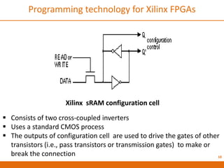
Programming technology for FPGAs
The logic cells within an FPGA are configured using a programming
technology. There are two classes of programming technology :
[i] OTP(One time programmable) [ii] Reprogrammable
Different FPGAs use different programmable (switching) elements :
[i] Antifuse in ACTEL FPGA
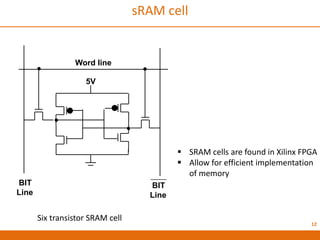
[ii] Static RAM cell in Xilinx FPGA
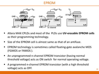
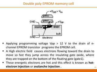
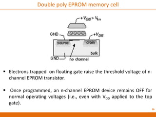
[iii] EPROM/ EEPROM in Altera CPLD
Programmable interconnect (PI) is used to connect any two logic
cells.
Different FPGAs use different interconnect architectures
[i] Segmented Channel routing in ACTEL FPGA
[ii] LCA interconnect architecture in Xilinx FPGA
3. 3
Antifuse technology for ACTEL FPGAs
An antifuse is the opposite of a regular fuse
An antifuse is a normally open(N.O) type of switch. A programming
current of 5 mA through it closes the switch.
e.g. In a poly-diffusion antifuse, the high current density causes a
large power dissipation in a small area, which melts a thin insulating
dielectric between polysilicon and diffusion electrodes and forms a
thin (about 20 nm in diameter), permanent, and resistive silicon.
Antifuses separate interconnect wires on FPGA and programmer
blows an antifuse to make a permanent connection. This
programming process cannot be reversed.
4. 4
Programming technology for ACTEL FPGAs
Actel’s Antifuse
Two types of antifuses are used :
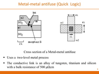
[i] Poly-diffusion antifuse (Actel) [ii] Metal-metal antifuse (Quick
Logic)
Actel calls its antifuse as Programmable Low Impedance Circuit
Element (PLICE)
Advantage: small area overhead (size of the antifuse switching
element is very small in comparison with size of sRAM cell)
Disadvantage : OTP
5. 5
ACTEL antifuse
A cross section of Actel antifuse
The ONO (oxide-nitride-oxide) dielectric layer having thickness less
than 10 nm is deposited between conducting polysilicon and
diffusion layers.
ONO dielectric is a combination of silicon dioxide and silicon nitride
2λ
6. 6
ACTEL antifuse
Actel antifuse (a) A cross section of a poly-diffusion antifuse (b) A
simplified drawing. The ONO (oxide–nitride–oxide) dielectric is less
than 10 nm thick, so this diagram is not to scale. (c) From above, an
antifuse is approximately the same size as a contact.
7. 7
ACTEL ‘s PLICE
• The size of an antifuse is limited by the resolution of the
lithography equipment used to makes ICs.
The fabrication process and the programming current
control the average resistance of a blown antifuse.
For programming current of 5 mA, antifuse resistance is
of the order of about 500 Ω. For 15 mA current, antifuse
resistance is about 100 Ω.
The number of antifuse switches used in an ACTEL FPGA
is large. Eg. An Actel 1010 contains 1,12,000 antifuses.
8. 8
Metal-metal antifuse (Quick Logic)
Cross section of a Metal-metal antifuse
Uses a two-level metal process
The conductive link is an alloy of tungsten, titanium and silicon
with a bulk resistance of 500 μΩcm
9. 9
Metal-metal antifuse
Advantages of metal-metal antifuse over poly-diffusion antifuse
(i) Connections form antifuses to wiring layers (metal) are direct.
Hence, associated parasitic capacitance is less.
(ii) Because of direct connection, area requirement is also reduced.
(i) Also due to direct connection, it is easier to use larger
programming current which results in reduced antifuse
resistance.
For Quick logic antifuse resistance is given by
R ≈ 0.8/ I Ω, where I in mA
Resistance of metal-metal antifuse is around 80 Ω for a
programming current of 15 mA (for quick logic).
10. 10
Programming technology for Xilinx FPGAs
Xilinx sRAM configuration cell
Consists of two cross-coupled inverters
Uses a standard CMOS process
The outputs of configuration cell are used to drive the gates of other
transistors (i.e., pass transistors or transmission gates) to make or
break the connection
11. 11
Xilinx sRAM configuration cell
Advantages:
Designers can reuse chips
Easy to upgrade the circuit design
Disadvantages:
Volatile and power supply should be kept applied (Alternatively,
the configuration data can be downloaded from a PROM or Flash
memory) every time the system is turned ON)
Larger in size
14. 14
EPROM
Altera MAX CPLDs and most of the PLDs use UV-erasable EPROM cells
as their programming technology.
Size of the EPROM cell is almost same as that of an antifuse.
EPROM technology is sometimes called floating-gate avalanche MOS
(FGMOS or FAMOS ).
An unprogrammed n-channel EPROM transistor (having normal
threshold voltage) acts as ON switch for normal operating voltage.
A programmed n-channel EPROM transistor (with a high threshold
voltage) acts as OFF.
15. 15
Double poly EPROM memory cell
Applying programming voltage Vpp > 12 V to the drain of n-
channel EPROM transistor programs the EPROM cell.
A High electric field causes electrons flowing toward the drain to
move so fast they jump across the insulating gate oxide, where
they are trapped on the bottom of the floating gate (gate1).
These energetic electrons are hot and this effect is known as hot-
electron injection or avalanche injection .
16. 16
Double poly EPROM memory cell
Electrons trapped on floating gate raise the threshold voltage of n-
channel EPROM transistor.
Once programmed, an n-channel EPROM device remains OFF for
normal operating voltages (i.e., even with VDD applied to the top
gate).
17. 17
Double poly EPROM memory cell
UV light is used to erase the EPROM cell. UV light provides
enough energy for the electrons stuck on gate1 to “jump” back to the
bulk, allowing the transistor to operate normally.
18. 18
EEPROM
Programming an EEPROM transistor is similar to programming
an UV-erasable EPROM transistor, but the erase mechanism is
different.
In an EEPROM transistor an electric field is also used to remove
electrons from the floating gate of a programmed transistor.
This is faster than using a UV lamp and the chip does not have to
be removed from the system.
19. 19
Actel ACT family interconnect
The channel routing uses dedicated rectangular areas of fixed size
within the chip called wiring channels or just channels.
The horizontal channels run across the chip in the horizontal direction.
The vertical channels run over the top of the basic logic cells in the
vertical direction .
Within the horizontal or vertical channels wires run horizontally or
vertically, respectively, within tracks.
The channel capacity refers to the number of tracks it contains. Each
track holds one wire.
In a channeled gate array the designer decides the location and length
of the interconnect within a channel. But, in an FPGA the interconnect
is fixed at the time of manufacture.
Each Logic Module is provided with the input stubs and output stubs.
21. 21
Segmented channel routing
To allow programming of the interconnect, Actel divides the fixed
interconnect wires within each channel into wires of various
lengths called wire segments.
This is referred as segmented channel routing, a type of channel
routing.
Antifuses join the wire segments. The designer then programs
the interconnections by blowing antifuses and making
connections between wire segments; unwanted connections are
left unprogrammed.
A statistical analysis of many different layouts determines the
optimum number and the lengths of the wire segments.
23. 23
Horizontal tracks
The ACT1 interconnection architecture uses a total of 25
tracks per channel ( 22 horizontal tracks per channel for
signal routing + 3 tracks dedicated to VDD, GND, and the
global clock (GCLK))
Horizontal segments vary in length from 4 columns of
Logic Modules to the entire row of modules (Actel calls
these long segments as long lines).
ACT1 interconnection architecture
24. 24
Vertical tracks
Each ACT1 logic module has 8 inputs ( 4 input stubs on top and 4 on
bottom)
8 vertical tracks per LM are available for inputs (4 from the LM above
the channel and 4 from the LM below).These connections are the input
stubs.
The single LM output connects to a vertical track that extends across
the 2 channels above the module and across the 2 channels below the
module (output stub). Since this is a dedicated connection, no antifuse
is needed.
Thus module outputs use 4 vertical tracks per module (counting 2 tracks
from the modules below, and 2 tracks from the modules above each
channel).
ACT1 interconnection architecture
25. 25
Vertical tracks
One vertical track per column is a long vertical track (
LVT ) that spans the entire height of the chip (Actel
1020 contains some segmented LVTs).
There are thus a total of 13 vertical tracks per column
in the ACT 1 architecture (8 for inputs, 4 for outputs,
and 1 for an LVT).
ACT1 interconnection architecture
26. 26
The ACT 1 devices are very nearly fully populated (an antifuse at
every horizontal and vertical interconnect intersection).
If the Logic Module at the end of a net is less than two rows away
from the driver module, a connection requires 2 antifuses, 1
vertical track, and 2 horizontal segments.
If the modules are more than two rows apart, a connection
between them will require a long vertical track (LVT) together with
another vertical track (the output stub) and two horizontal tracks.
To connect these tracks will require a total of 4 antifuses in series
and this will add delay due to the resistance of the antifuses.
ACT1 interconnection architecture
27. 27
Xilinx LCA
The vertical lines and horizontal lines run between CLBs.
The general-purpose interconnect joins switch boxes (also known
as magic boxes or switching matrices).
The long lines run across the entire chip. It is possible to form
internal buses using long lines and the three-state buffers that are
next to each CLB.
The direct connections (not used on the XC4000) bypass the
switch matrices and directly connect adjacent CLBs.
The Programmable Interconnection Points (PIP’s) are
programmable pass transistors that connect the CLB inputs and
outputs to the routing network.
The bidirectional (BIDI) interconnect buffers restore the logic level
and logic strength on long interconnect paths.
28. 28
Xilinx LCA
Xilinx LCA interconnect. (a) The LCA architecture (notice the matrix element size is
larger than a CLB). (b) A simplified representation of the interconnect resources.
Each of the lines is a bus.
29. 29
Components of interconnect delay in a Xilinx LCA array. (a) A portion of the interconnect
around the CLBs. (b) A switching matrix. (c) A detailed view inside the switching matrix
showing the passtransistor arrangement. (d) The equivalent circuit for the connection
between nets 6 and 20 using the matrix. (e) A view of the interconnect at a Programmable
Interconnection Point (PIP). (f) and (g) The equivalent schematic of a PIP connection.
30. 30
Altera MAX 5000 and 7000 Interconnect scheme
A simplified block diagram of the Altera MAX interconnect scheme. (a) The PIA
(Programmable Interconnect Array) is deterministic— delay is independent of the
path length. (b) Each LAB (Logic Array Block) contains a programmable AND array.
31. 31
Altera MAX Interconnect scheme
• Altera MAX 5000/7000 devices use a Programmable
Interconnect Array ( PIA ).
• The PIA is a cross-point switch for logic signals traveling
between LABs.
• The advantages of this architecture is it uses a fixed
number of connections so the routing delay is also
fixed.
• Simpler and regular structure in nature that improved
speed of the placement and routing software.
• The delay between LAB1 and LAB2 is the same as the
delay between LAB1 and LAB6