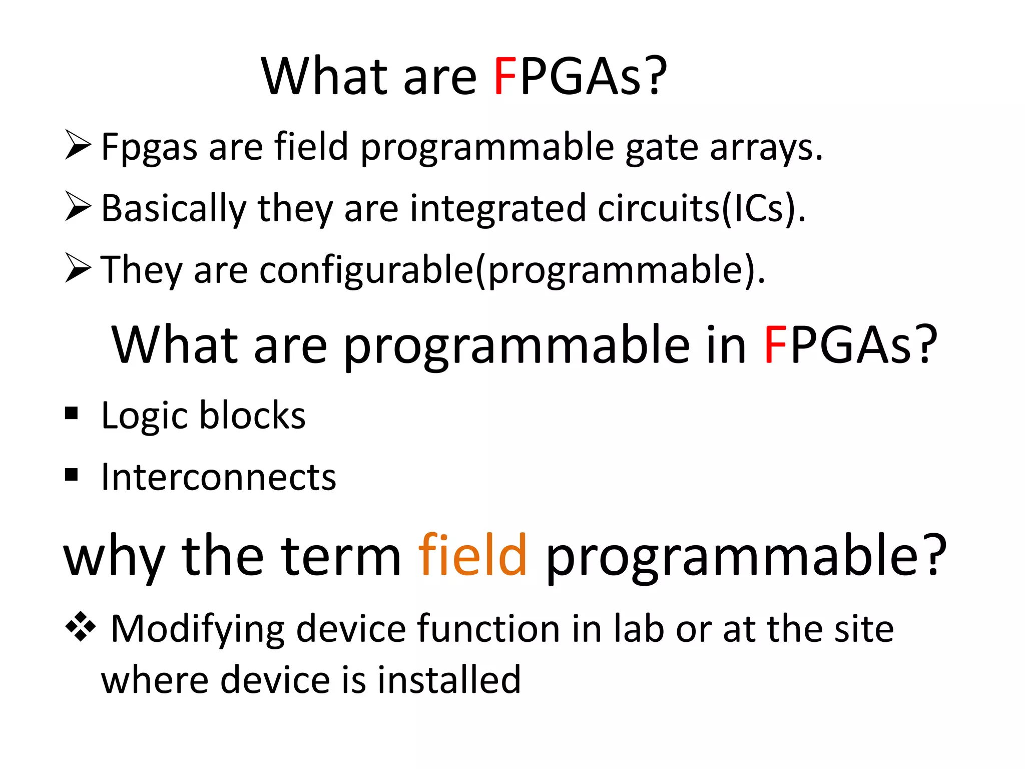
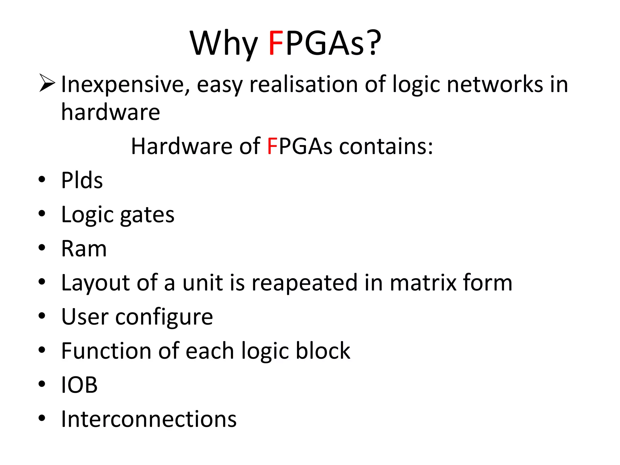
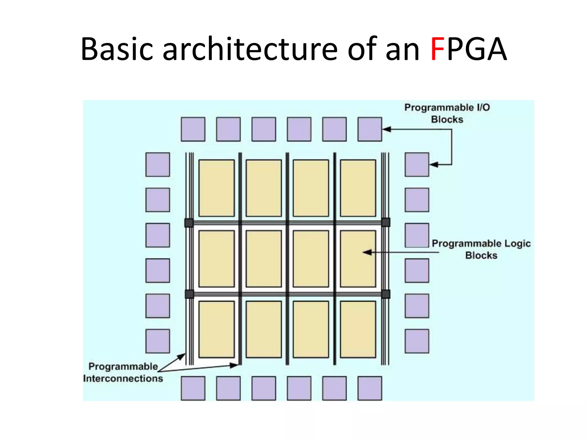
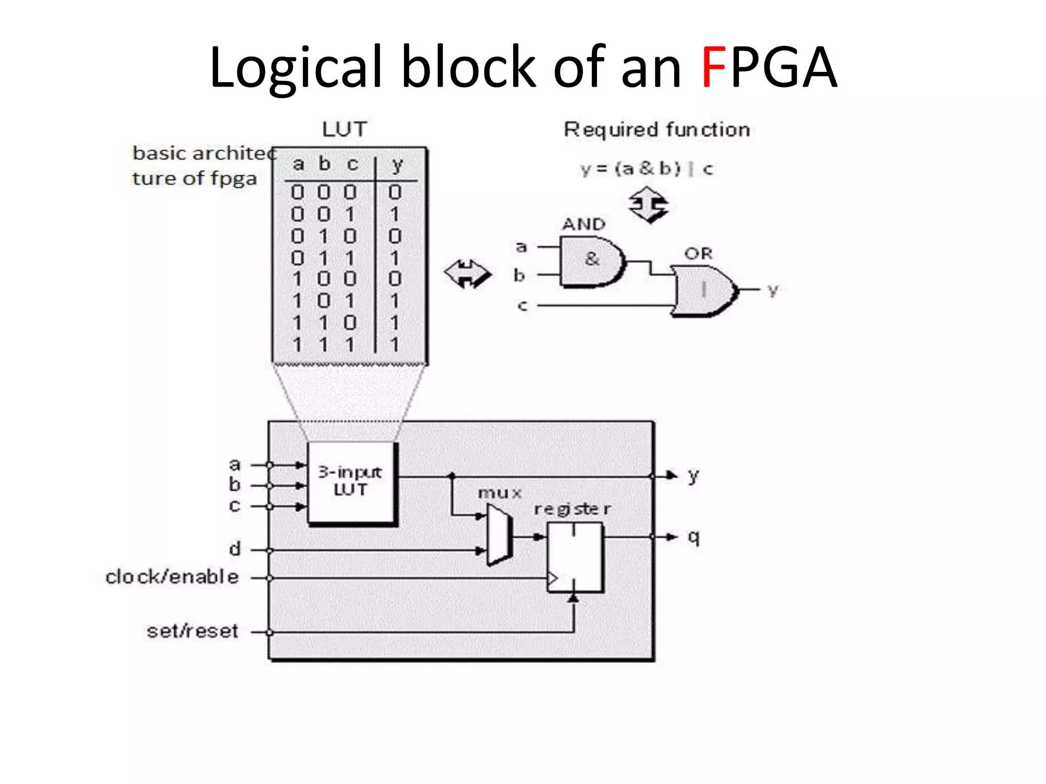
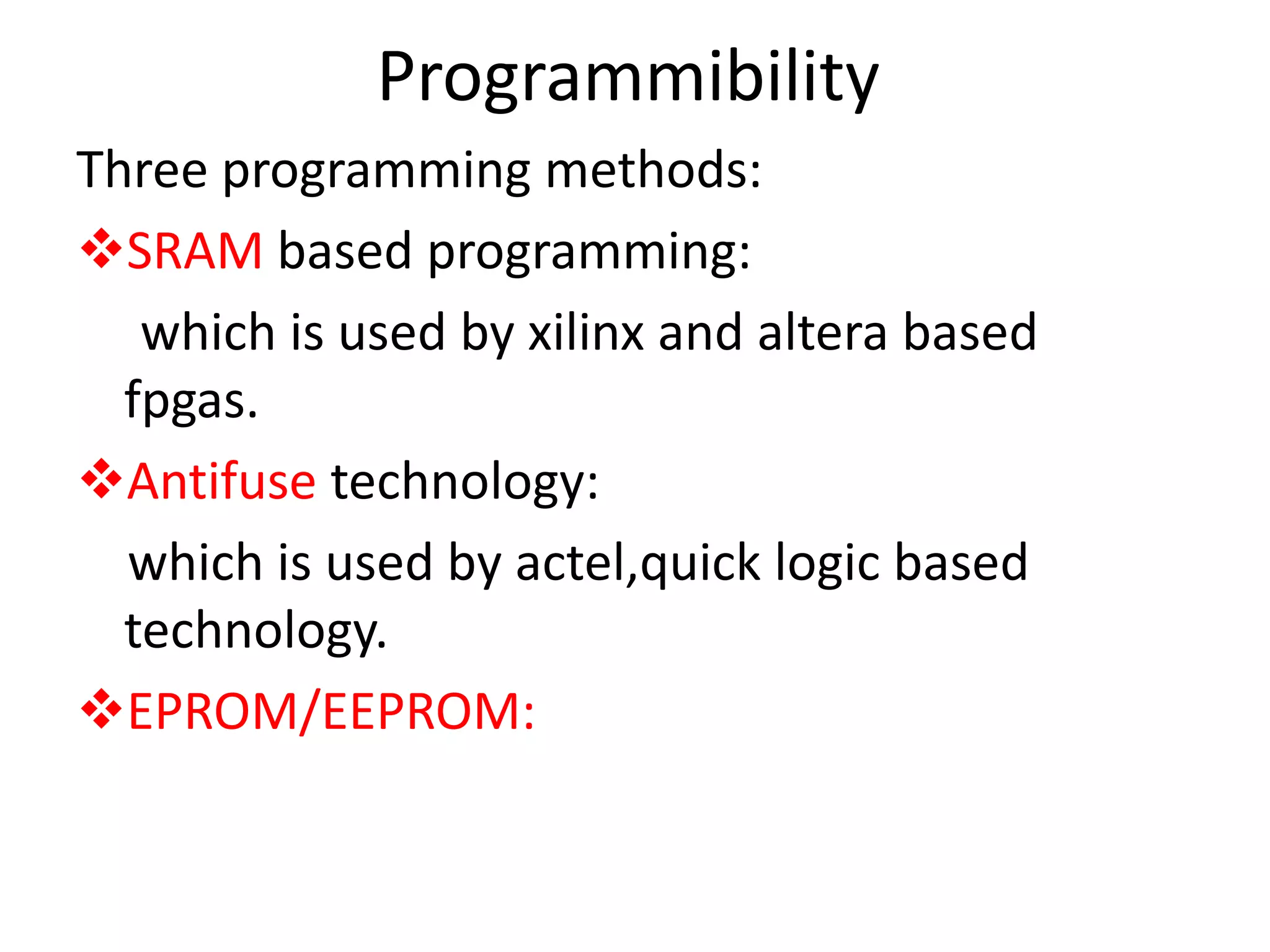
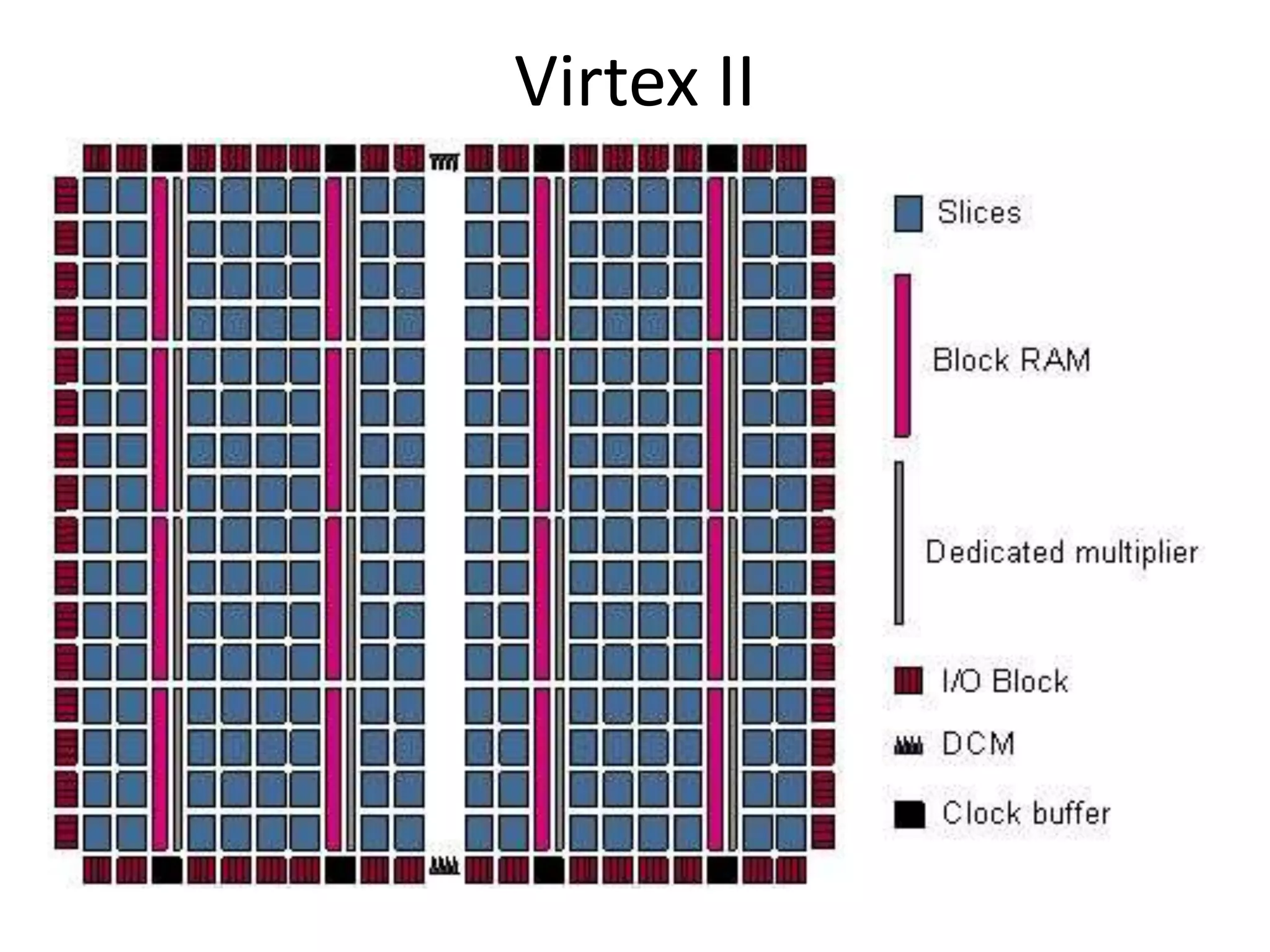
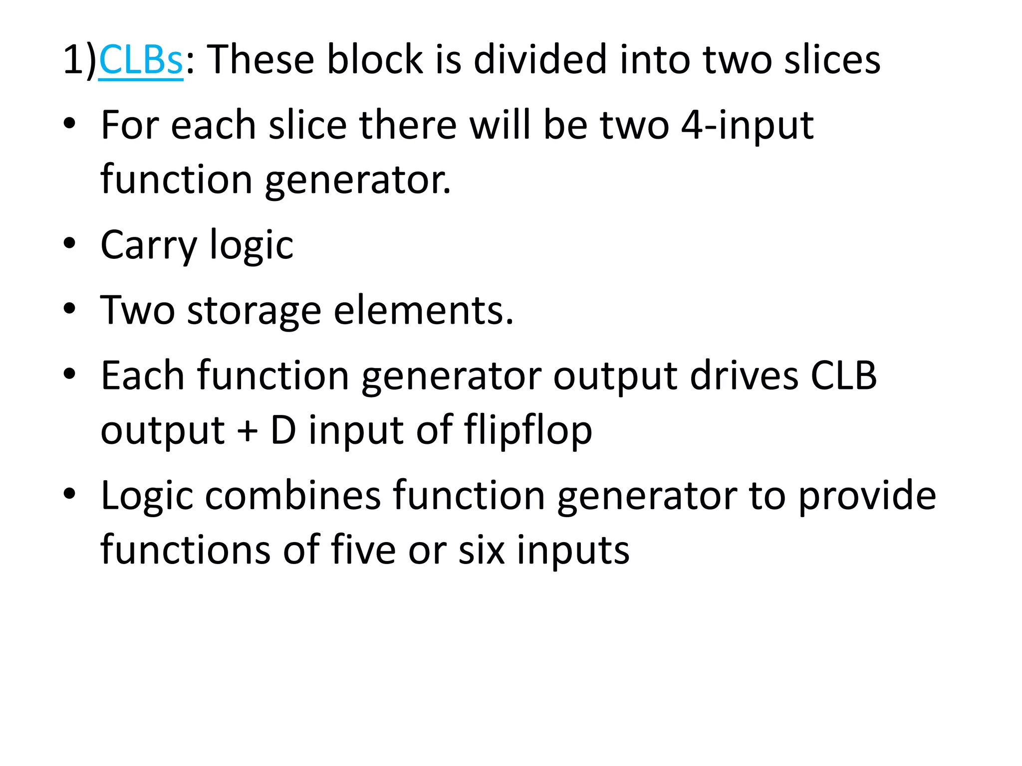
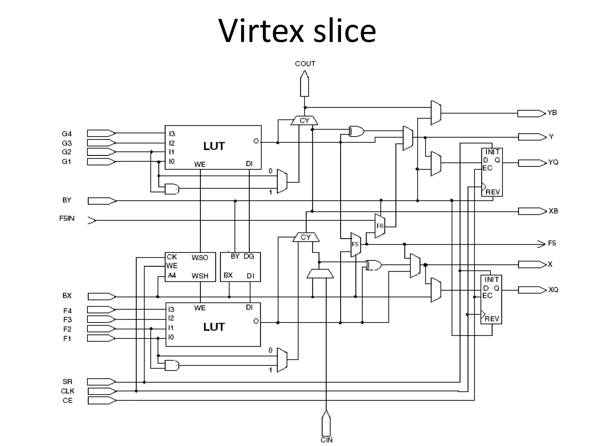
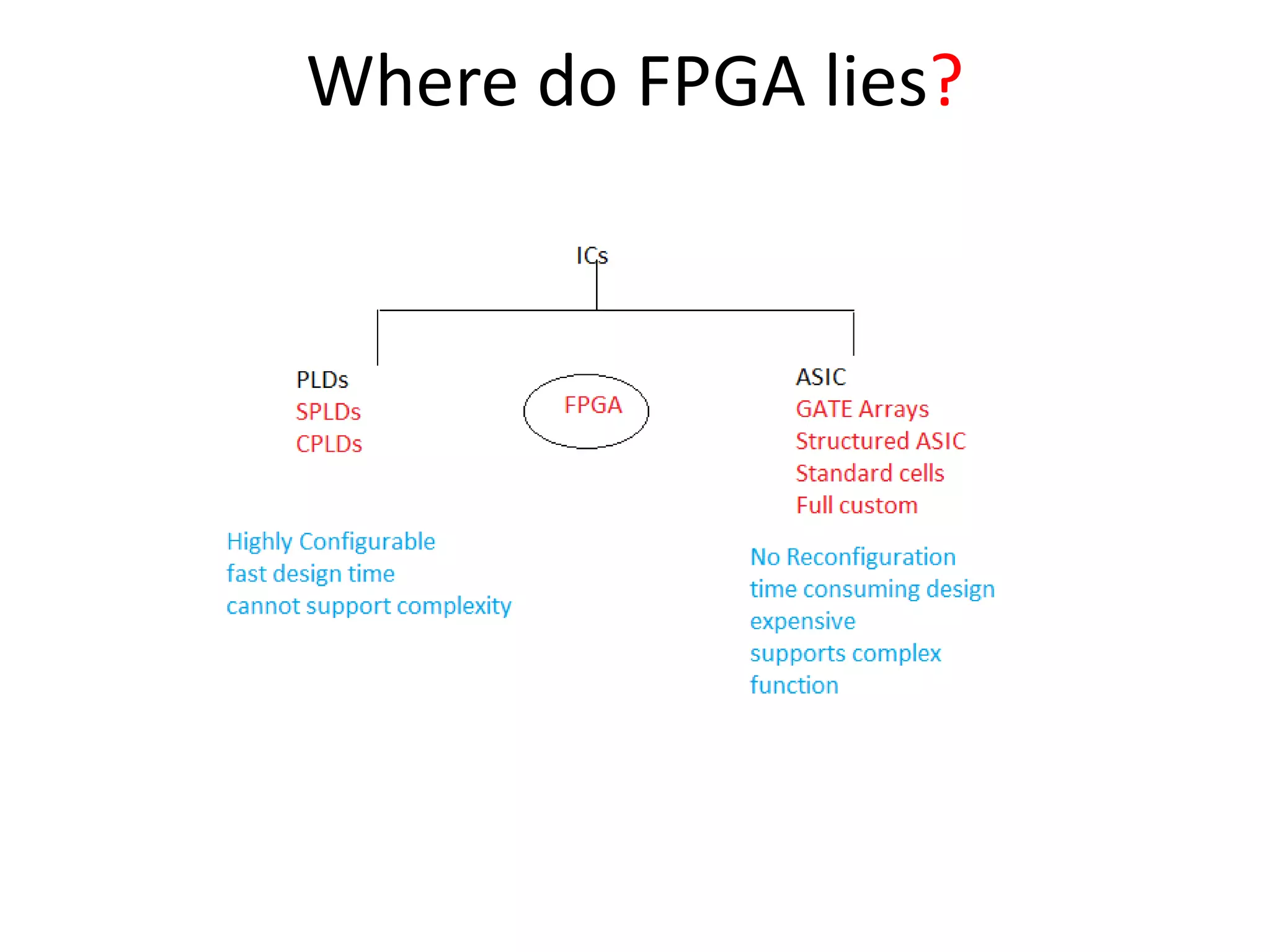
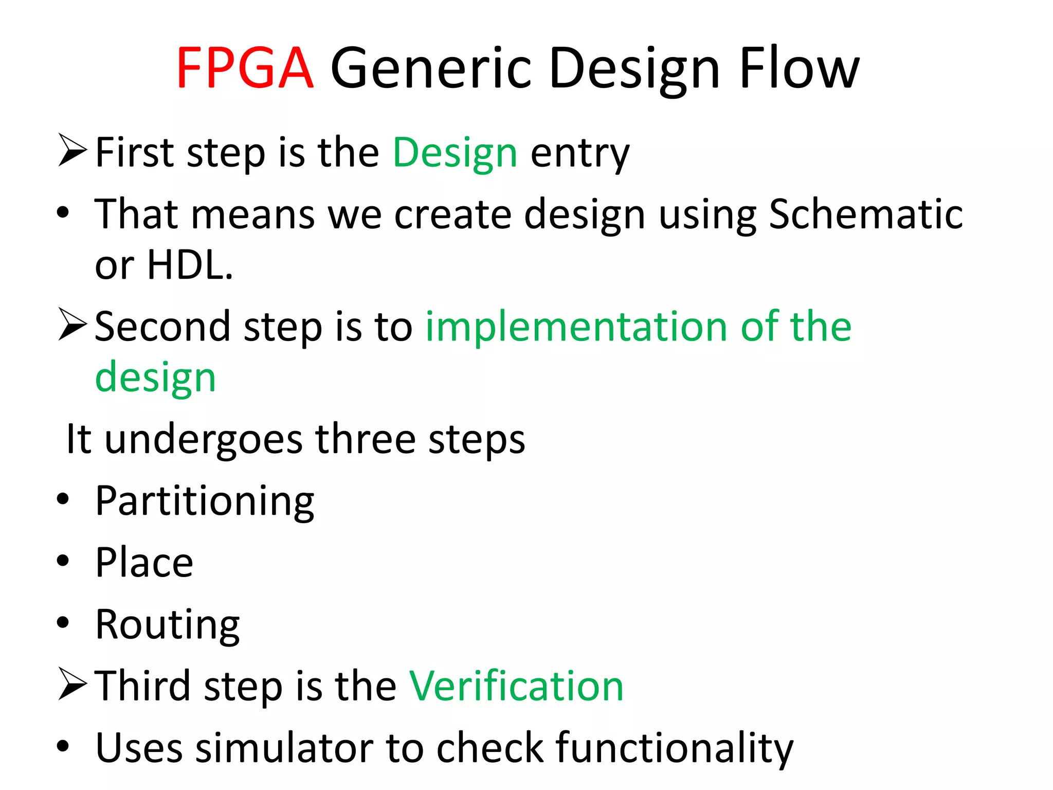
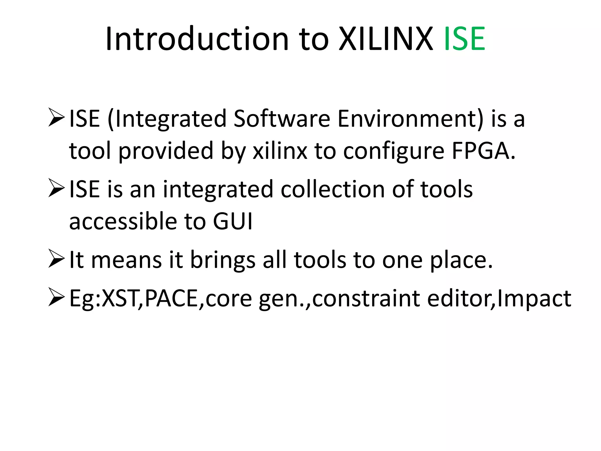
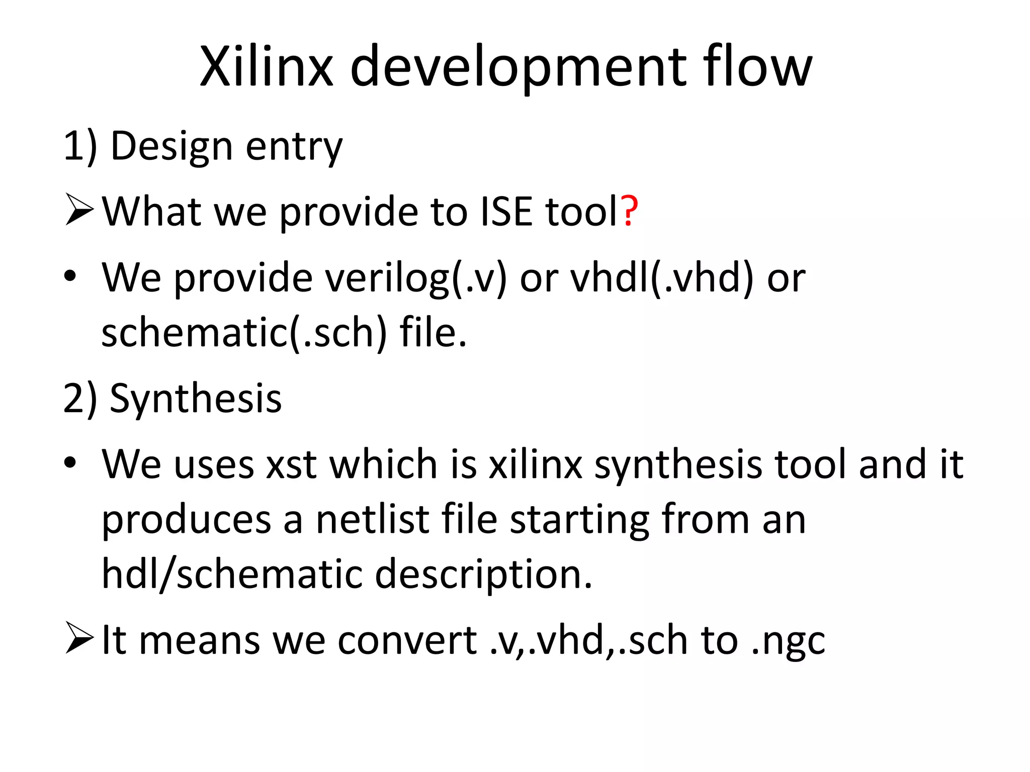
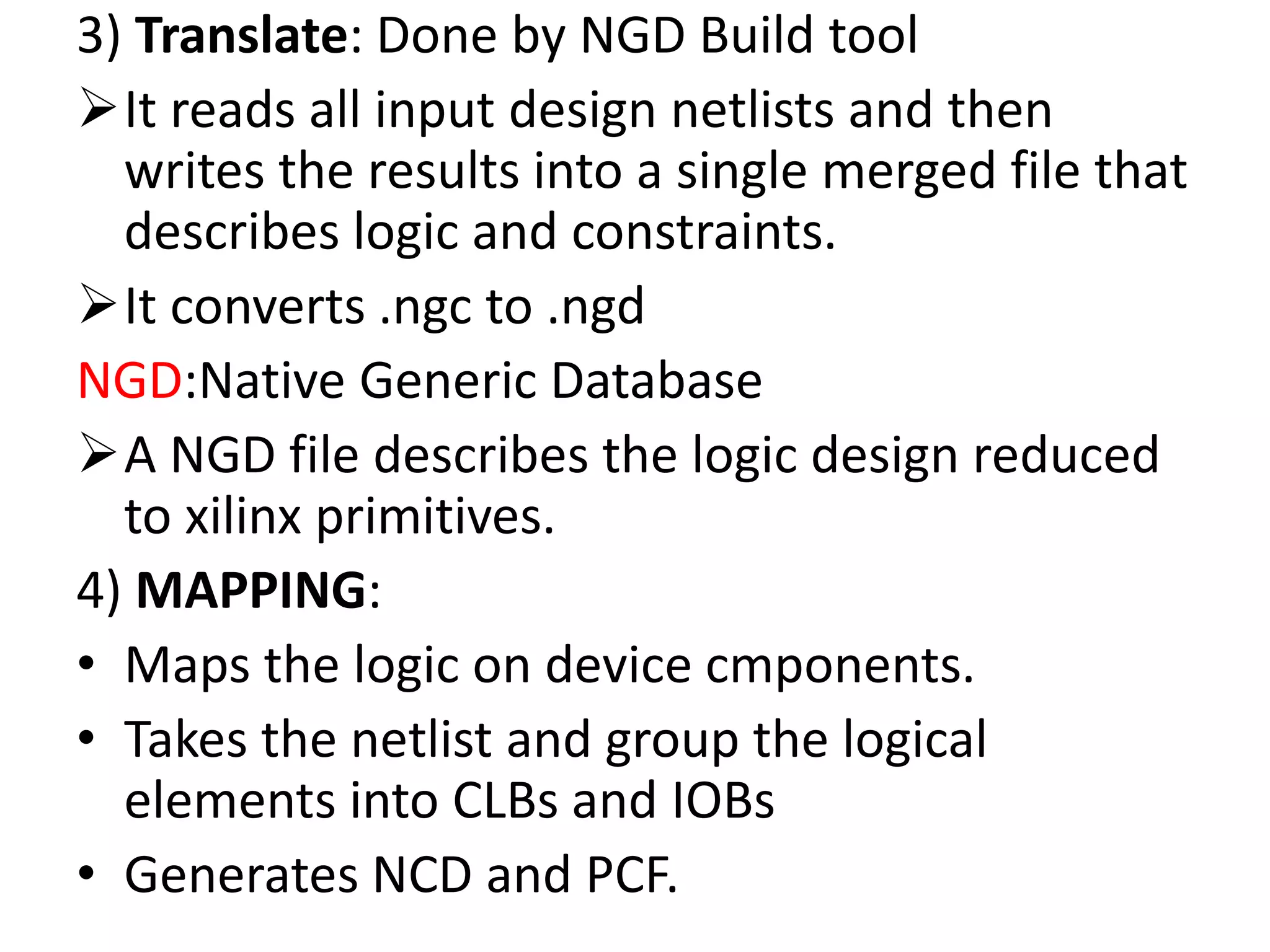
FIELD PROGRAMMABLE GATE
ARRAYS
BY
GOPIREDDY BHARADWAJAREDDY
PONDICHERRY UNIVERSITY
CONTENTS
What are FPGAs?
Families of FPGA
Basic architecture of FPGA
Programmability
Xilinx specifications
Fpga generic design flow
Introduction to xilinx ISE
Xilinx devolepment flow
What are FPGAs?
Fpgas are field programmable gate arrays.
Basically they are integrated circuits(ICs).
They are configurable(programmable).
What are programmable in FPGAs?
 Logic blocks
 Interconnects
why the term field programmable?
 Modifying device function in lab or at the site
where device is installed
Why FPGAs?
Inexpensive, easy realisation of logic networks in
hardware
Hardware of FPGAs contains:
• Plds
• Logic gates
• Ram
• Layout of a unit is reapeated in matrix form
• User configure
• Function of each logic block
• IOB
• Interconnections
Families of FPGAs
Xilinx
Actel
Altera
What was difference between the above three
FPGAs families?
• Physical means for implementing
programmabilty.
• Interconnection among arrangments.
• Basic functionality of logic blocks.
Basic architecture of an FPGA
Logical block of an FPGA
Programmibility
Three programming methods:
SRAM based programming:
which is used by xilinx and altera based
fpgas.
Antifuse technology:
which is used by actel,quick logic based
technology.
EPROM/EEPROM:
S-Ram based programming
Fpga connections:
• Pass transistors
• Transmission gates
• Multipliers
Making or breaking cross point connections
Define function of logic blocks
How an SRAM is programmed?
There are two pins i.e; input/output
configurable pins which are used to program
When we implement a logic into fpga it is
converted into bit files which was stored
serially(as a single shift register) from input to
output.
programability
• Interconnect lines are pre-laid
vertically and horizontally.
• Programmable switches connects
the lines to input/output of
logic blocks.
• A switch matrix is a set of multi-
plexers where an incoming line con-
nected to any outgoing line.
Antifuse technology
• It is a one time programming
Antifuse:links in configurable paths
 In an unprogrammed state it acts as like a high
impedance
Xilinx specifications
Xilinx provides many FPGAs that differ in complexity
which is based in number of configurable logical
blocks.
There are two types of fpgas
1)Virtex II based FPGA
2)Spartan 3E based FPGA
Although they differ in complexity,all FPGAs
contains similar structure like,
CLBs:configurable logic blocks
IOBSs:input/output blocks
PI:programmable interconnects
Ram blocks
Buffers etc.;
Virtex II
1)CLBs: These block is divided into two slices
• For each slice there will be two 4-input
function generator.
• Carry logic
• Two storage elements.
• Each function generator output drives CLB
output + D input of flipflop
• Logic combines function generator to provide
functions of five or six inputs
Virtex slice
IOBs
The IOBs appears as a storage elements that
acts as either D-ff or Latches.
Ther are certain modes in which IOBs work
1)Snchronous set/reset.
2)Asynchronous preset/clear.
Each IOB can be programmed into
1)Input path: In this the Buffer routes input
signal directly to core or via D-ff.
2)Output path:In this Buffer routes output signal
directly from core or via D-ff.
RAM Blocks
Blocks of RAMs are organized in columns.
Why ram?
• To store any intermediate data in an
application.
Programmable routing
How this programmable routing takes place?
• Adajacent to each CLB stands a General
Routing Matrix(GRM).
• GRM is nothing but switch matrix which get
resources from CLBs,RAM,Multipliers.
Arithmetic resources in xilinx FPGAs
• Some arithmetic resources like
adders,counters,multipliers are required
because special circuitry to speed up
arithmetic operations.
• Dedicated carry logic/xor
Where do FPGA lies?
FPGA Generic Design Flow
First step is the Design entry
• That means we create design using Schematic
or HDL.
Second step is to implementation of the
design
It undergoes three steps
• Partitioning
• Place
• Routing
Third step is the Verification
• Uses simulator to check functionality
Introduction to XILINX ISE
ISE (Integrated Software Environment) is a
tool provided by xilinx to configure FPGA.
ISE is an integrated collection of tools
accessible to GUI
It means it brings all tools to one place.
Eg:XST,PACE,core gen.,constraint editor,Impact
Xilinx development flow
1) Design entry
What we provide to ISE tool?
• We provide verilog(.v) or vhdl(.vhd) or
schematic(.sch) file.
2) Synthesis
• We uses xst which is xilinx synthesis tool and it
produces a netlist file starting from an
hdl/schematic description.
It means we convert .v,.vhd,.sch to .ngc
3) Translate: Done by NGD Build tool
It reads all input design netlists and then
writes the results into a single merged file that
describes logic and constraints.
It converts .ngc to .ngd
NGD:Native Generic Database
A NGD file describes the logic design reduced
to xilinx primitives.
4) MAPPING:
• Maps the logic on device cmponents.
• Takes the netlist and group the logical
elements into CLBs and IOBs
• Generates NCD and PCF.
NCD:Native Circuit Description File
Gives information about the physical circuit
description of input design as applied to a specific
device.
PCF:physical constraints file
Contains information about physical constraints
5)Place and route:
• Determines the placement of cells and the
routing between the cells.
6)Bit stream generation:
• A Bit stream is a stream of data that contains the
location information for logic on a device.
7)configuration/programming:
• Programming a bit file into fpga using JTAG port.
There are some other tools that are used by xilinx ISE:
o HDL compiler which uses XST tool to compile given
input.
o For simulation xilinx ISEsim,modelsim are used.
o Core generator and architecture wizard.
o Pinout and area constraint editor uses PACEtool to
maka a constraint for a given circuit.
o Implementation is done by using Translate/Map/Par.
o Device configuration is done by Impact tool.
FURTHER DISCUSSION
APPLICATIONS OF FPGA.
THANK YOU

Fpga

  • 1.
    FIELD PROGRAMMABLE GATE ARRAYS BY GOPIREDDYBHARADWAJAREDDY PONDICHERRY UNIVERSITY
  • 2.
    CONTENTS What are FPGAs? Familiesof FPGA Basic architecture of FPGA Programmability Xilinx specifications Fpga generic design flow Introduction to xilinx ISE Xilinx devolepment flow
  • 3.
    What are FPGAs? Fpgasare field programmable gate arrays. Basically they are integrated circuits(ICs). They are configurable(programmable). What are programmable in FPGAs?  Logic blocks  Interconnects why the term field programmable?  Modifying device function in lab or at the site where device is installed
  • 4.
    Why FPGAs? Inexpensive, easyrealisation of logic networks in hardware Hardware of FPGAs contains: • Plds • Logic gates • Ram • Layout of a unit is reapeated in matrix form • User configure • Function of each logic block • IOB • Interconnections
  • 5.
    Families of FPGAs Xilinx Actel Altera Whatwas difference between the above three FPGAs families? • Physical means for implementing programmabilty. • Interconnection among arrangments. • Basic functionality of logic blocks.
  • 6.
  • 7.
  • 8.
    Programmibility Three programming methods: SRAMbased programming: which is used by xilinx and altera based fpgas. Antifuse technology: which is used by actel,quick logic based technology. EPROM/EEPROM:
  • 9.
    S-Ram based programming Fpgaconnections: • Pass transistors • Transmission gates • Multipliers Making or breaking cross point connections Define function of logic blocks
  • 10.
    How an SRAMis programmed? There are two pins i.e; input/output configurable pins which are used to program When we implement a logic into fpga it is converted into bit files which was stored serially(as a single shift register) from input to output.
  • 11.
    programability • Interconnect linesare pre-laid vertically and horizontally. • Programmable switches connects the lines to input/output of logic blocks. • A switch matrix is a set of multi- plexers where an incoming line con- nected to any outgoing line.
  • 12.
    Antifuse technology • Itis a one time programming Antifuse:links in configurable paths  In an unprogrammed state it acts as like a high impedance
  • 13.
    Xilinx specifications Xilinx providesmany FPGAs that differ in complexity which is based in number of configurable logical blocks. There are two types of fpgas 1)Virtex II based FPGA 2)Spartan 3E based FPGA Although they differ in complexity,all FPGAs contains similar structure like, CLBs:configurable logic blocks IOBSs:input/output blocks PI:programmable interconnects Ram blocks Buffers etc.;
  • 14.
  • 15.
    1)CLBs: These blockis divided into two slices • For each slice there will be two 4-input function generator. • Carry logic • Two storage elements. • Each function generator output drives CLB output + D input of flipflop • Logic combines function generator to provide functions of five or six inputs
  • 16.
  • 17.
    IOBs The IOBs appearsas a storage elements that acts as either D-ff or Latches. Ther are certain modes in which IOBs work 1)Snchronous set/reset. 2)Asynchronous preset/clear. Each IOB can be programmed into 1)Input path: In this the Buffer routes input signal directly to core or via D-ff. 2)Output path:In this Buffer routes output signal directly from core or via D-ff.
  • 18.
    RAM Blocks Blocks ofRAMs are organized in columns. Why ram? • To store any intermediate data in an application. Programmable routing How this programmable routing takes place? • Adajacent to each CLB stands a General Routing Matrix(GRM). • GRM is nothing but switch matrix which get resources from CLBs,RAM,Multipliers.
  • 19.
    Arithmetic resources inxilinx FPGAs • Some arithmetic resources like adders,counters,multipliers are required because special circuitry to speed up arithmetic operations. • Dedicated carry logic/xor
  • 20.
  • 21.
    FPGA Generic DesignFlow First step is the Design entry • That means we create design using Schematic or HDL. Second step is to implementation of the design It undergoes three steps • Partitioning • Place • Routing Third step is the Verification • Uses simulator to check functionality
  • 22.
    Introduction to XILINXISE ISE (Integrated Software Environment) is a tool provided by xilinx to configure FPGA. ISE is an integrated collection of tools accessible to GUI It means it brings all tools to one place. Eg:XST,PACE,core gen.,constraint editor,Impact
  • 23.
    Xilinx development flow 1)Design entry What we provide to ISE tool? • We provide verilog(.v) or vhdl(.vhd) or schematic(.sch) file. 2) Synthesis • We uses xst which is xilinx synthesis tool and it produces a netlist file starting from an hdl/schematic description. It means we convert .v,.vhd,.sch to .ngc
  • 24.
    3) Translate: Doneby NGD Build tool It reads all input design netlists and then writes the results into a single merged file that describes logic and constraints. It converts .ngc to .ngd NGD:Native Generic Database A NGD file describes the logic design reduced to xilinx primitives. 4) MAPPING: • Maps the logic on device cmponents. • Takes the netlist and group the logical elements into CLBs and IOBs • Generates NCD and PCF.
  • 25.
    NCD:Native Circuit DescriptionFile Gives information about the physical circuit description of input design as applied to a specific device. PCF:physical constraints file Contains information about physical constraints 5)Place and route: • Determines the placement of cells and the routing between the cells. 6)Bit stream generation: • A Bit stream is a stream of data that contains the location information for logic on a device.
  • 26.
    7)configuration/programming: • Programming abit file into fpga using JTAG port. There are some other tools that are used by xilinx ISE: o HDL compiler which uses XST tool to compile given input. o For simulation xilinx ISEsim,modelsim are used. o Core generator and architecture wizard. o Pinout and area constraint editor uses PACEtool to maka a constraint for a given circuit. o Implementation is done by using Translate/Map/Par. o Device configuration is done by Impact tool.
  • 27.
  • 28.