Download as PDF, PPTX


![Slide 19Subhash Iyer, Program Head, Soft Polynomials (I) Pvt. Ltd
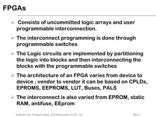
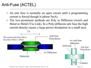
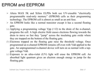
EEPROM
Creating a wired-AND with EPROM cells [3]
Structure of a FAMOS transistor [3]
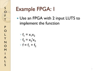
F= A + B + C + D + …….
= A . B . C . D . ……..
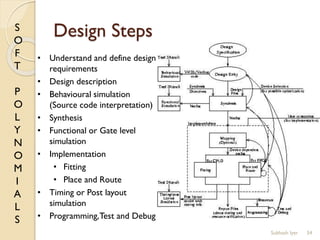
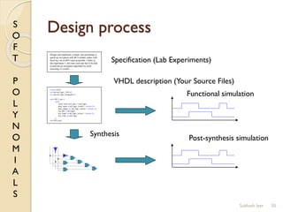
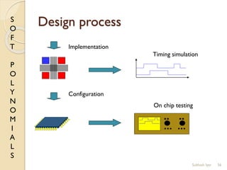
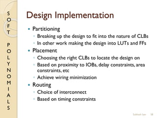
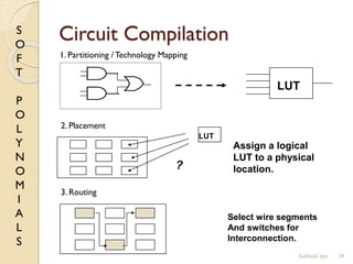
First Level
Polysilicon
Second Level
Polysilicon
Field Oxide
Gate Oxide](https://image.slidesharecdn.com/fcaf3c08-0cfa-4bf0-8fe6-7ac889b944e5-160223160543/85/Session-2-3-FPGAs-100-320.jpg)
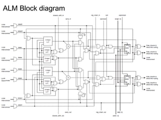
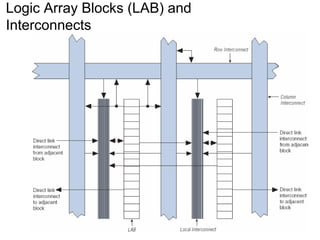


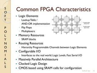
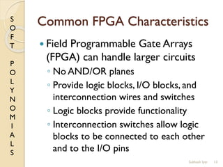
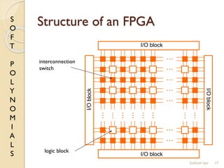
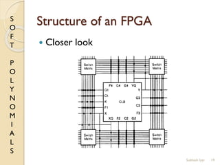
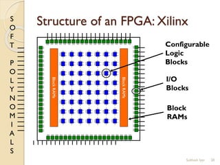
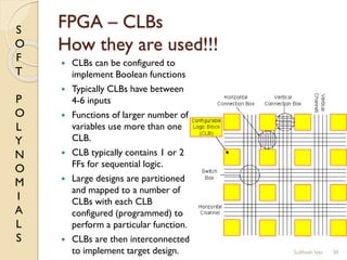
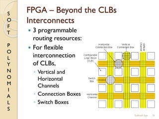
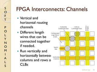
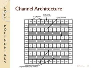
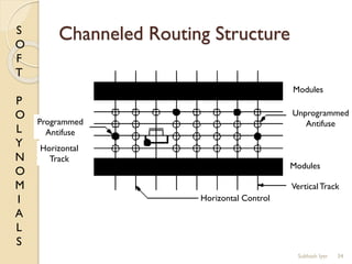
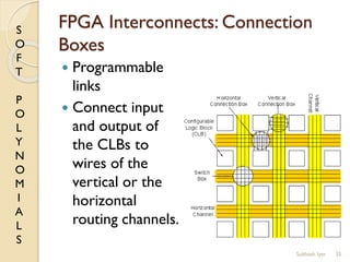
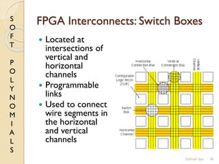
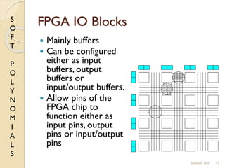
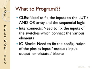
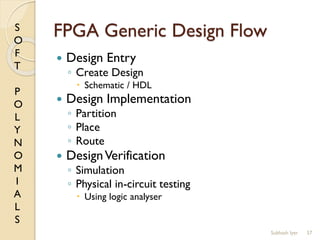
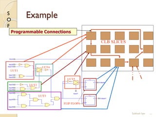
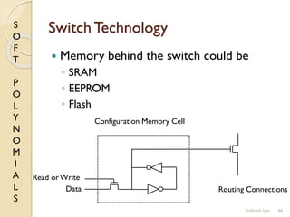
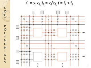
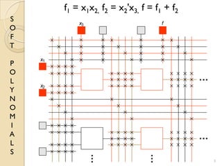
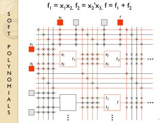
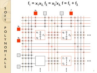
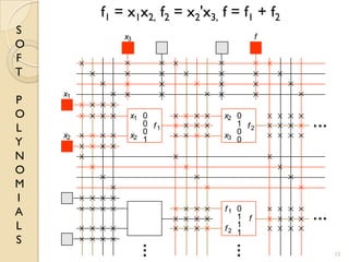
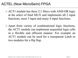
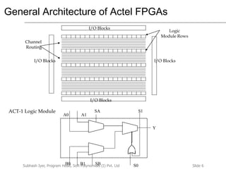
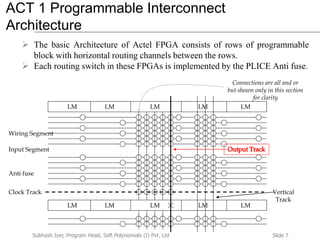
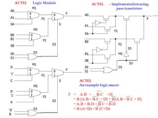
The document discusses the structure and components of field programmable gate arrays (FPGAs). FPGAs consist of programmable logic blocks, interconnects, and input/output blocks. The logic blocks contain lookup tables and flip flops that can be programmed to implement desired logic functions. The interconnects include vertical and horizontal routing channels and switch boxes that allow the logic blocks to be connected as needed. The input/output blocks provide interfaces between the FPGA and external devices.